S i 5 2 11 2 - A 1 / A 2
PCI-E XPRESS G EN 1 DUAL O UTPUT C LOCK G ENERATOR
Features
PCI-Express Gen 1 compliant
Low power HCSL differential
output buffers
Supports Serial-ATA (SATA) at
100 MHz
No termination resistors required
25 MHz Crystal Input or Clock
input
Triangular spread spectrum
profile for maximum EMI
reduction (Si52112-A2)
Extended Temperature:
–40 to 85 °C
3.3 V Power supply
Small package 10-pin TDFN
(3x3 mm)
Si52112-A1 does not support
spread spectrum outputs
Si52112-A2 supports 0.5% down
spread outputs
For PCIe Gen 2 applications, see
Si52112-B3/B4
For PCIe Gen 3 applications, see
Si52112-B5/B6
Ordering Information:
See page 13
Pin Assignments
Applications
Network Attached Storage
Multi-function Printer
Wireless Access Point
Routers
VDD
VDD
1
10
XOUT
2
9
DIFF2
XIN/CLKIN
3
8
DIFF2
VSS
4
7
DIFF1
VSS
5
6
DIFF1
Description
Si52112-A1/A2 is a high-performance, PCIe clock generator that can
source two PCIe clocks from a 25 MHz crystal or clock input. The clock
outputs are compliant to PCIe Gen 1 specifications. The ultra-small
footprint (3x3 mm) and industry leading low power consumption make
Si52112-A1/A2 the ideal clock solution for consumer and embedded
applications.
Patents pending
VDD
DIFF1
XIN/CLKIN
PLL
Divider
DIFF2
XOUT
VSS
Rev 1.2 7/14
Copyright © 2014 by Silicon Laboratories
Si52112-A1/A2
�Si52112-A1/A2
2
Rev 1.2
�Si52112-A1/A2
TABLE O F C ONTENTS
Section
Page
1. Electrical Specifications . . . . . . . . . . . . . . . . . . . . . . . . . . . . . . . . . . . . . . . . . . . . . . . . . . .4
2. Crystal Recommendations . . . . . . . . . . . . . . . . . . . . . . . . . . . . . . . . . . . . . . . . . . . . . . . . .7
2.1. Crystal Loading . . . . . . . . . . . . . . . . . . . . . . . . . . . . . . . . . . . . . . . . . . . . . . . . . . . . . .7
2.2. Calculating Load Capacitors . . . . . . . . . . . . . . . . . . . . . . . . . . . . . . . . . . . . . . . . . . . .8
3. Test and Measurement Setup . . . . . . . . . . . . . . . . . . . . . . . . . . . . . . . . . . . . . . . . . . . . . . .9
4. Pin Descriptions . . . . . . . . . . . . . . . . . . . . . . . . . . . . . . . . . . . . . . . . . . . . . . . . . . . . . . . . . 11
4.1. 10-Pin TDFN . . . . . . . . . . . . . . . . . . . . . . . . . . . . . . . . . . . . . . . . . . . . . . . . . . . . . . . 11
4.2. 8-Pin TSSOP . . . . . . . . . . . . . . . . . . . . . . . . . . . . . . . . . . . . . . . . . . . . . . . . . . . . . . . 12
5. Ordering Guide . . . . . . . . . . . . . . . . . . . . . . . . . . . . . . . . . . . . . . . . . . . . . . . . . . . . . . . . . . 13
6. Package Outlines . . . . . . . . . . . . . . . . . . . . . . . . . . . . . . . . . . . . . . . . . . . . . . . . . . . . . . . .14
6.1. TDFN Package . . . . . . . . . . . . . . . . . . . . . . . . . . . . . . . . . . . . . . . . . . . . . . . . . . . . . 14
6.2. TSSOP Package . . . . . . . . . . . . . . . . . . . . . . . . . . . . . . . . . . . . . . . . . . . . . . . . . . . . 16
7. Recommended Design Guideline . . . . . . . . . . . . . . . . . . . . . . . . . . . . . . . . . . . . . . . . . . . 18
Document Change List . . . . . . . . . . . . . . . . . . . . . . . . . . . . . . . . . . . . . . . . . . . . . . . . . . . . .19
Contact Information . . . . . . . . . . . . . . . . . . . . . . . . . . . . . . . . . . . . . . . . . . . . . . . . . . . . . . . .20
Rev 1.2
3
�Si52112-A1/A2
1. Electrical Specifications
Table 1. Recommended Operating Conditions
Parameter
Symbol
Test Condition
Min
Typ
Max
Unit
VDD(extended)
3.3 V ± 5%
3.13
3.3
3.46
V
VDD(commercial)
3.3 V ± 10%
2.97
3.3
3.63
V
Symbol
Test Condition
Min
Typ
Max
Unit
Operating Voltage
VDD
3.3 V ± 10%
2.97
3.30
3.63
V
Operating Supply Current
IDD
Full Active
—
—
17
mA
Input Pin Capacitance
CIN
Input Pin Capacitance
—
3
5
pF
COUT
Output Pin Capacitance
—
—
5
pF
Supply Voltage (extended)
Supply Voltage (commercial)
Table 2. DC Electrical Specifications
Parameter
Output Pin Capacitance
4
Rev 1.2
�Si52112-A1/A2
Table 3. AC Electrical Specifications
Parameter
Symbol
Test Condition
Min
Typ
Max
Unit
LACC
Measured at VDD/2 differential
—
—
250
ppm
TDC
Measured at VDD/2
45
—
55
%
CLKIN Rise and Fall Times
TR/TF
Measured between 0.2 VDD and
0.8 VDD
0.5
—
4.0
V/ns
CLKIN Cycle-to-Cycle Jitter
TCCJ
Measured at VDD/2
—
—
250
ps
CLKIN Long Term Jitter
TLTJ
Measured at VDD/2
—
—
350
ps
Input High Voltage
VIH
XIN/CLKIN pin
2
—
VDD+0.3
V
Input Low Voltage
VIL
XIN/CLKIN pin
—
—
0.8
V
Input High Current
IIH
XIN/CLKIN pin, VIN = VDD
—
—
35
uA
Input Low Current
IIL
XIN/CLKIN pin, 0 < VIN
很抱歉,暂时无法提供与“SI52112-A1-GM2”相匹配的价格&库存,您可以联系我们找货
免费人工找货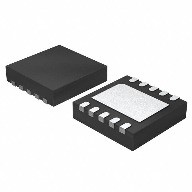


 工商网监
湘ICP备2023018690号
工商网监
湘ICP备2023018690号
