Si5338
I 2 C - P R O G R A M M A B LE A N Y - F R E Q U E N C Y, A N Y -O UTPU T Q U A D C L OC K G E N E R A T O R
Features
CLK0A
CLK0B
VDD
VDDO0
20
Low power MultiSynth™ technology enables independent, any-frequency synthesis on four differential output drivers Highly-configurable output drivers with up to four differential outputs, eight single-ended clock outputs, or a combination of both Low phase jitter of 0.7 ps RMS typ High precision synthesis allows true zero ppm frequency accuracy on all outputs Flexible input reference: External crystal: 8 to 30 MHz CMOS input: 5 to 200 MHz SSTL/HSTL input: 5 to 350 MHz Differential input: 5 to 710 MHz Independently configurable outputs support any frequency or format: LVPECL/LVDS: 0.16 to 710 MHz HCSL: 0.16 to 250 MHz CMOS: 0.16 to 200 MHz SSTL/HSTL: 0.16 to 350 MHz Independent output voltage per driver: 1.5, 1.8, 2.5, or 3.3 V
RSVD_GND
I2C/SMBus compatible interface Easy to use programming software Small size: 4 x 4 mm, 24-QFN Low power: 45 mA core supply typ Wide temperature range: –40 to +85 °C
24
23
22
21
19 18 CLK1A 17 CLK1B 16 VDDO1 15 VDDO2 14 CLK2A 13 CLK2B
IN1 1 IN2 2 IN3 3 IN4 4 IN5 5 GND GND Pad
Applications
Ethernet switch/router PCI Express 2.0/3.0 Broadcast video/audio timing Processor and FPGA clocking
Any-frequency clock conversion MSAN/DSLAM/PON Fibre Channel, SAN Telecom line cards
IN6 6
7 8 9 10 11 12
INTR
Description
The Si5338 is a high-performance, low-jitter clock generator capable of synthesizing any frequency on each of the device's four output drivers. This timing IC is capable of replacing up to four different frequency crystal oscillators or operating as a frequency translator. Using its patented MultiSynth™ technology, the Si5338 allows generation of four independent clocks with 0 ppm precision. Each output clock is independently configurable to support various signal formats and supply voltages. The Si5338 provides low-jitter frequency synthesis in a space-saving 4 x 4 mm QFN package. The device is programmable via an I2C/ SMBus-compatible serial interface and supports operation from a 1.8, 2.5, or 3.3 V core supply. I2C device programming is made easy with the ClockBuilder™ Desktop software available at www.silabs.com/ClockBuilder.
Rev. 0.6 9/10
Copyright © 2010 by Silicon Laboratories
VDDO3
CLK3B
CLK3A
VDD
SCL
SDA
Single supply core with excellent PSRR: 1.8, 2.5, 3.3 V Independent frequency increment/ decrement feature enables glitchless frequency adjustments in 1 ppm steps Independent phase adjustment on each of the output drivers with an accuracy of 18 MHz
–45 — –45 — 667
Notes: 1. Outputs at integer-related frequencies and using the same driver format. See "3.9.3. Initial Phase Offset" on page 24. 2. The maximum step size is only limited by the register lengths; however, the MultiSynth output frequency must be kept between 5 MHz and Fvco/8. 3. Update rate via I2C is also limited by the time it takes to perform a write operation. 4. Default value is 0.5% down spread. 5. Default value is ~31.5 kHz.
6
Rev. 0.6
�S i5338
Table 5. Performance Characteristics (Continued)
(VDD = 1.8 V –5% to +10%, 2.5 V ±10%, or 3.3 V ±10%, TA = –40 to 85 °C)
Parameter Phase Increment/Decrement Update Time
Symbol PUPDATE
Test Condition Pin control2,3 MultiSynth output 18 MHz Pin control2,3 MultiSynth output 5 MHz. 6. Measured in accordance with JEDEC standard 65. 7. Rj is multiplied by 14; estimate the pp jitter from Rj over 212 rising edges.
12
Rev. 0.6
�S i5338
Table 12. Jitter Specifications1,2 (Continued)
(VDD = 1.8 V –5% to +10%, 2.5 V ±10%, or 3.3 V ±10%, TA = –40 to 85 °C)
Parameter
Symbol
Test Condition Output MultiSynth operated in fractional
Min —
Typ 3
Max 15
Unit ps pk-pk
Deterministic Jitter
DJ
mode
5
Output MultiSynth operated in integer mode5 Output MultiSynth operated in fractional mode5 Output MultiSynth operated in integer mode5
—
2
10
ps pk-pk
—
13
36
ps pk-pk
Total Jitter (12 kHz–20 MHz)
TJ = DJ+14xRJ (See Note 7)
—
12
20
ps pk-pk
Notes: 1. All jitter measurements apply for LVDS/HCSL/LVPECL output format with a low noise differential input clock and are made with an Agilent 90804 oscilloscope. All RJ measurements use RJ/DJ separation. 2. For best jitter performance, keep the single ended clock input slew rates at Pins 3 and 4 more than 1.0 V/ns and the differential clock input slew rates more than 0.3 V/ns. 3. DJ for PCI and GBE is < 5 ps pp 4. Output MultiSynth in Integer mode. 5. Input frequency to the Phase Detector between 25 and 40 MHz and any output frequency > 5 MHz. 6. Measured in accordance with JEDEC standard 65. 7. Rj is multiplied by 14; estimate the pp jitter from Rj over 212 rising edges.
Table 13. Typical Phase Noise Performance
Offset Frequency 100 Hz 1 kHz 10 kHz 100 kHz 1 MHz 10 MHz 25MHz XTAL to 156.25 MHz –90 –120 –126 –132 –132 –145 27 MHz Ref In to 148.3517 MHz –87 –117 –123 –130 –132 –145 19.44 MHz Ref In to 155.52 MHz –110 –116 –123 dBc/Hz –128 –128 –145 Units
Rev. 0.6
13
�S i5338
Table 14. I2C Specifications (SCL,SDA)1
Parameter Symbol Test Condition Standard Mode Min LOW Level Input Voltage HIGH Level Input Voltage Hysteresis of Schmitt Trigger Inputs LOW Level Output Voltage (open drain or open collector) at 3 mA Sink Current Input Current Capacitance for each I/O Pin I2C Bus Timeout VILI2C VIHI2C VHYS –0.5 0.7 x VDDI2C N/A Max 0.3 x VDDI2C 3.63 N/A Min –0.5 0.7 x VDDI2C2 0.1 Fast Mode Max 0.3 x VDDI2C2 3.63 — V V V Unit
VOLI2C2
VDDI2C2 = 2.5/3.3 V VDDI2C2 = 1.8 V
0 N/A
0.4 N/A
0 0
0.4 0.2 x VDDI2C
V V
II2C CI2C — VIN = –0.1 to VDDI2C Timeout Enabled
–10 — 25
10 4 35
–10 — 25
10 4 35
µA pF ms
Notes: 1. Refer to NXP’s UM10204 I2C-bus specification and user manual, Revision 03, for further details: www.nxp.com/acrobat_download/usermanuals/UM10204_3.pdf. 2. Only I2C pullup voltages (VDDI2C) of 1.71 to 3.63 V are supported. Must write register 27[7] = 1 if the I2C bus voltage is less than 2.5 V to maintain compatibility with the I2C bus standard.
14
Rev. 0.6
�S i5338
2. Typical Application Circuits
+3.3 V 0.1 uF Power Supply Decoupling Capacitors (1 per VDD or VDDOx pin)
7 24 VDD VDD 20 16 VDDOA VDDOB 15 11 VDDOC VDDOD
SD/HD/3G-SDI Video/Audio Format Converter
SD/HD/3G SDI IN SDI Deserializer Video Processor SDI Serializer SD/HD/3G SDI OUT
Optional XTAL for Free-run Applications
27 MHz XTAL
1 2
IN1 IN2
Single-ended or Differential Inputs for Synchronous Applications
27 MHz 74.25 MHz 74.25/1.001 MHz 148.5 MHz 148.5/1.001 MHz +3.3 V 1k 1k
3 5
IN3 IN5
CLK0A CLK0B
22 21 18 17
100 MHz
100
x
100
6 IN6
Si5338C
CLK1A CLK1B
74.25 MHz, 74.25/1.001 MHz 148.5 MHz, 148.5/1.001 MHz
CLK2A
14 13
1k
8 INTR SDA SCL GND 19 12 4
CLK2B
x x
Audio Out Audio Processor 24.576 MHz / 6.144 MHz
IN3
I C Bus I C Address = 111 0000 or 111 0001
2
2
CLK3A CLK3B
10 9
x
23 23
PAD PAD
GND
I2C_LSB
Storage Area Network
+3.3 V 0.1 uF Power Supply Decoupling Capacitors (1 per VDD or VDDOx pin)
7 24 VDD VDD 20 16 VDDOA VDDOB 15 11 VDDOC VDDOD
disk
disk
SAS2 4/8 Port Controller PCIe Switch Ethernet Fiber Channel
disk
25 MHz XTAL
1 2
IN1 IN2
SAS2 4/8 Port Controller
disk
3
IN3 IN5 IN6
CLK0A CLK0B
22 21 18 17
37.5/75/120/150 MHz
x
5 6
Si5338C
CLK1A CLK1B
100 MHz
x
66 MHz
+3.3V 1k I2C Bus I2C Address = 111 0000 or 111 0001 1k 1k
8 19 12 4 INTR SDA SCL GND
CLK2A CLK2B
14 13
Network Processor
x
106.25 MHz
CLK3A CLK3B
10 9
x
23 23
PAD PAD
Rev. 0.6
GND
I2C_LSB
15
�S i5338
3. Functional Description
VDD Input Stage Synthesis Stage 1 (PLL) Synthesis Stage 2 MultiSynth ÷M0
ref
Osc
Output Stage VDDO0 ÷R0 CLK0A CLK0B VDDO1
IN1 IN2 IN3
CLKIN
÷P1 Phase Frequency Detector
fb
Loop Filter
VCO
FDBK
MultiSynth ÷M1
÷R1
CLK1A CLK1B VDDO2
IN4 IN5 IN6
÷P2 MultiSynth ÷M2 Control & Memory
OEB/PINC/FINC I2C_LSB/PDEC/FDEC
÷R2
CLK2A CLK2B VDDO3
MultiSynth ÷N MultiSynth ÷M3 ÷R3
CLK3A CLK3B
SCL SDA INTR
Control
NVM RAM (OTP)
Figure 1. Si5338 Block Diagram
3.1. Overview
The Si5338 is a high-performance, low-jitter clock generator capable of synthesizing four independent user-programmable clock frequencies up to 350 MHz and select frequencies up to 710 MHz. The device supports free-run operation using an external crystal, or it can lock to an external clock for generating synchronous clocks. The output drivers support four differential clocks or eight single-ended clocks or a combination of both. The output drivers are configurable to support common signal formats, such as LVPECL, LVDS, HCSL, CMOS, HSTL, and SSTL. Separate output supply pins allow supply voltages of 3.3, 2.5, 1.8, and 1.5 V to support the multi-format output driver. The core voltage supply accepts 3.3, 2.5, or 1.8 V and is independent from the output supplies. Using its two-stage synthesis architecture and patented high-resolution MultiSynth technology, the Si5338 can generate four independent frequencies from a single input frequency. In addition to clock generation, the inputs can bypass the synthesis stage enabling the Si5338 to be used as a high-performance clock buffer or a combination of a buffer and generator. For applications that need fine frequency adjustments, such as clock margining, each of the synthesized frequencies can be incremented or decremented in user-defined steps as low as 1 ppm per step. Output-to-output phase delays are also adjustable in user-defined steps with an error of Save Register Map File or Options > Save C code Header File, or create the register contents by the conversions listed in AN411. 3.5.3. Writing a Custom Configuration to RAM Writing a new configuration (register map) to the RAM consists of pausing the LOL state-machine, writing new values to the IC accounting for the write-allowed mask given in "6.1. Register Write-Allowed Mask" on page 28, validating the input clock or crystal, locking the PLL to the input with the new configuration, restarting the LOL state-machine, and calibrating the VCO for robust operation across temperature. The flow chart in Figure 9 on page 21 enumerates the details:
Note: The write-allowed mask specifies which bits must be read and modified before writing the entire register byte (a.k.a. read-modify-write). “AN428: Jump Start: InSystem, Flash-Based Programming for Silicon Labs’ Timing Products” illustrates the procedure defined in Section 3.5.2 with ANSI C code.
20
Rev. 0.6
�S i5338
Disable Outputs Set OEB_ALL = 1; reg230[4]
Pause LOL Set DIS_LOL = 1; reg241[7]
Register Map Use ClockBuilder Desktop v2.7 or later
Write new configuration to device accounting for the write-allowed mask (See Section 6.1)
Validate input clock status Input clocks are validated with the LOS alarms. See Register 218 to determine which LOS should be monitored NO Is input clock valid? YES Configure PLL for locking Set FCAL_OVRD_EN = 0; reg49[7]
Initiate Locking of PLL Set SOFT_RESET = 1; reg246[1]
Restart LOL Set DIS_LOL = 0; reg241[7]
Wait 25 ms
Confirm PLL lock status NO PLL is locked when PLL_LOL, SYS_CAL, and all other alarms are cleared Is PLL locked? YES Copy FCAL values to active registers Copy registers as follows: 237[1:0] to 47[1:0] 236[7:0] to 46[7:0] 235[7:0] to 45[7:0] Set 47[7:2] = 000101b
Set PLL to use FCAL values Set FCAL_OVRD_EN = 1; reg49[7]
Enable Outputs Set OEB_ALL = 0; reg230[4]
Figure 9. I2C Programming Procedure
Rev. 0.6
21
�S i5338
3.5.4. Modifying a MultiSynth Output Divider Ratio/ Frequency Configuration The output MultiSynth dividers of a configured and phase-locked Si5338 can be modified without relocking the PLL (i.e. without following section 3.5.3). This feature allows any of the four output frequencies to be modified without disturbing the others. In this case, only write the set of registers associated with the output MultiSynth divider (MultiSynth Frequency Configuration; see Section 6.2). The feedback MultiSynth must not be modified unless following the procedure in Section 3.5.3. To avoid intermediate frequencies, it is recommended that the output be disabled before changing the divider ratio (see Register 230). Any output MultiSynth that is reconfigured will lose its phase alignment with the other outputs. SOFT_RESET can be used to resynchronize the outputs (see "3.8. Reset Options" on page 23). 3.5.5. Writing a Custom Configuration to NVM An alternative to ordering an Si5338 with a custom NVM configuration is to use the field programming kit (Si5338-PROG-EVB) to write directly to the NVM of a "blank" Si5338. Since NVM is an OTP memory, it can only be written once. The default configuration can be reconfigured by writing to RAM through the I2C interface (see “3.5.2. Creating a New Configuration for RAM”). 3.6.1. Using the INTR Pin in Systems with I2C The INTR output pin is not latched and thus it should not be a polled input to an MCU but an edge-triggered interrupt. An MCU can process an interrupt event by reading the sticky register 247 to see what event caused the interrupt. The same register can be cleared by writing zeros to the bits that were set. Individual interrupt bits can be masked by register 6[4:0]. 3.6.2. Using the INTR Pin in Systems without I2C The INTR pin also provides a useful function in systems that require a pin-controlled fault indicator. Pre-setting the interrupt mask register allows the INTR pin to become an indicator for a specific event, such as LOS and/or LOL. Therefore, the INTR pin can be used to indicate a single fault event or even multiple events.
Control & Memory VDD
1k
INTR
Control
NVM RAM (OTP)
Figure 11. INTR Pin with Required Pull-Up
3.7. Output Enable
There are two methods of enabling and disabling the output drivers: Pin control, and I2C control. 3.7.1. Enabling Outputs Using Pin Control The Si5338K/L/M devices provide an Output Enable pin (OEB) as shown in Figure 12. Pulling this pin high will turn all outputs off. The state of the individual drivers when turned off is controllable. If an individual output is set to always on, then the OEB pin will not have an effect on that driver. Drive state options and always on are explained in “3.7.2. Enabling Outputs through the I2C Interface”.
Control & Memory
3.6. Status Indicators
A logic-high interrupt pin (INTR) is available to indicate a loss of signal (LOS) condition, a PLL loss of lock (PLL_LOL) condition, or that the PLL is in process of acquiring lock (SYS_CAL). PLL_LOL is held high when the input frequency drifts beyond the PLL lock range. It is held low during all other times and during a POR or soft reset. SYS_CAL is held high during a POR or SOFT reset so that no chattering occurs during the locking process. As shown in Figure 10, a status register at address 218 is available to help identify the exact event that caused the interrupt pin to become active.
7 6 5 4 3 2 1 0 Sys Cal System Calibration (Lock Acquisition) Loss Of Signal Clock Input Loss Of Signal Feedback Input Loss Of Lock
218
PLL_LOL LOS_FDBK LOS_CLKIN
Control 0 = Enabled 1 = Disabled OEB
NVM RAM (OTP)
Figure 12. Output Enable Pin (Si5338K/L/M)
Figure 10. Status Register
Figure 11 shows a typical connection with the required pull-up resistor to VDD.
22
Rev. 0.6
�S i5338
3.7.2. Enabling Outputs through the I2C Interface Output enable can be controlled through the I2C interface. As shown in Figure 13, register 230[3:0] allows control of each individual output driver. Register 230[4] controls all drivers at once. When register 230[4] is set to disable all outputs, the individual output enables will have no effect. Registers 110[7:6], 114[7:6], 118[7:6], and 112[7:6] control the output disabled state as tri-state, low, high, or always on. If always on is set, that output will always be on regardless of any other register or chip state. In addition, the always on mode must be selected for an output that is fed back in a Zero Delay application.
7 6 5 4 3 2 1 0
3.8. Reset Options
There are two types of resets on the Si5338, POR and soft reset. A POR reset automatically occurs whenever the supply voltage on the VDD is applied. The soft reset is forced by writing 0x02 to register 246. This bit is not self-clearing, and thus it may read back as a 1 or a 0. A soft reset will not download any preprogrammed NVM and will not change any register values in RAM. The soft reset performs the following sequence: 1. All outputs turn off except if programmed to be always on. 2. Internal calibrations are done and MultiSynths are initialized. a. Outputs that are synchronous are phase aligned (if Rn = 1). 3. 25 ms is allowed for the PLL to lock (no delay occurs when FCAL_OVRD_EN = 1). 4. Turn on all outputs that were turned off in step 1.
230
OEB OEB OEB OEB OEB All 3 2 1 0 0 = enable 1 = disable
Bits reserved
3.9. Features of the Si5338
7 6 5 4 3 2 1 0
110
CLK0 OEB State
7
6
5
4
3
2
1
0
114
CLK1 OEB State
The Si5338 offers several features and functions that are useful in many timing applications. The following paragraphs describe in detail the main features and typical applications. All of these features can be easily configured using the ClockBuilder Desktop. See "3.1.1. ClockBuilder™ Desktop Software" on page 16. 3.9.1. Frequency Increment/Decrement Each of the output clock frequencies can be independently stepped up or down in predefined steps as low as 1 ppm per step and with a resolution of 1 ppm. Setting of the step size and control of the frequency increment or decrement is accomplished through the I2C interface. Alternatively, the Si5338 can be ordered with optional frequency increment (FINC) and frequency decrement (FDEC) pins for pincontrolled applications. See Table 18 for ordering information of pin-controlled devices. The frequency increment and decrement feature is useful in applications requiring a variable clock frequency (e.g., CPU speed control, FIFO overflow management, etc.) or in applications where frequency margining (e.g., fout ±5%) is necessary for design verification and manufacturing test. Frequency increment or decrement can be applied as fast as 1.5 MHz when it is done by pin control. When under I2C control, the frequency increment and decrement update rate is limited by the I2C bus speed. The magnitude of the frequency step has 0 ppm error. Frequency steps are seamless and glitchless.
7
6
5
4
3
2
1
0
118
CLK2 OEB State
7
6
5
4
3
2
1
0
122
CLK3 OEB State
00 = disabled tri-state 01 = disabled low 10 = disabled high 11 = always enabled
Bits used by other functions
Figure 13. Output Enable Control Registers
Rev. 0.6
23
�S i5338
3.9.2. Output Phase Increment/Decrement The Si5338 has a digitally-controlled glitchless phase increment and decrement feature that allows adjusting the phase of each output clock in relation to the other output clocks. The phase of each output clock can be adjusted with an accuracy of 20 ps over a range of ±45 ns. Setting of the step size and control of the phase increment or decrement is accomplished through the I2C interface. Alternatively, the Si5338 can be ordered with optional phase increment (PINC) and phase decrement (PDEC) pins for pin-controlled applications. In pin controlled applications the phase increment and decrement update rate is as fast as 1.5 MHz. In I2C applications, the maximum update rate is limited by the speed of the I2C. See Table 18 for ordering information of pin-controlled devices. The phase increment and decrement feature provides a useful method for fine tuning setup and hold timing margins or adjusting for mismatched PCB trace lengths. 3.9.3. Initial Phase Offset Each output clock can be set for its initial phase offset up to ±45 ns. In order for the initial phase offset to be applied correctly at power up, the VDDOx output supply voltage must cross 1.2 V before the VDD (pins 7,24) core power supply voltage crosses 1.45 V. This applies to the each driver output individually. A soft_reset will also guarantee that the programmed Initial Phase Offset is applied correctly. The initial phase offset only works on outputs that have their R divider set to 1. 3.9.4. Output R Divider When the requested output frequency of a channel is below 5 MHz, the Rn (n = 0,1,2,3) divider needs to be set and enabled. This is automatically done in register maps generated by the ClockBuilder Desktop. When the Rn divider is active the step size range of the frequency increment and decrement function will decrease by the Rn divide ratio. The Rn divider can be set to {1, 2, 4, 8, 16, 32}. Non-unity settings of R0 will affect the Finc/Fdec step size at the MultiSynth0 output. For example, if the MultiSynth0 output step size is 2.56 MHz and R0 = 8, the step size at the output of R0 will be 2.56 MHz divided by 8 = .32 MHz. When the Rn divider is set to non-unity, the initial phase of the CLKn output with respect to other CLKn outputs is not guaranteed. 3.9.5. Zero-Delay Mode The Si5338 supports an optional zero delay mode of operation for applications that require minimal input-tooutput delay. In this mode, one of the device output clocks is fed back to the feedback input pin (IN4 or IN5/ IN6) to implement an external feedback path essentially nullifying the delay between the reference input and the output clocks. Figure 14 shows the Si5338 in a typical zero-delay configuration. It is generally recommended that Clk3 be LVDS and that the feedback input be pins 5 and 6. For the differential input configuration to pins 5 and 6, see Figure 3 on page 17. The zero-delay mode combined with the phase increment/decrement feature allows unprecedented flexibility in generating clocks with precise edge alignment.
Si5338
M0
R0
Clk0
Clk Input
P1 PLL P2
M1
R1
Clk1
M2
R2
Clk2
M3
R3
Clk3
Figure 14. Si5338 in Zero Delay Clock Generator Mode
24
Rev. 0.6
�S i5338
3.9.6. Spread Spectrum To help reduce electromagnetic interference (EMI), the Si5338 supports spread spectrum modulation. The output clock frequencies can be modulated to spread energy across a broader range of frequencies, lowering system EMI. The Si5338 implements spread spectrum using its patented MultiSynth technology to achieve previously unattainable precision in both modulation rate and spreading magnitude as shown in Figure 15. Spread spectrum can be applied to any output clock, any clock frequency, and any spread amount. The device supports center spread (±0.1% to ±5%) and down spread (–0.1% to –5%). In addition, the device has extensive on-chip voltage regulation so that power supply variations do not influence the device’s spreadspectrum clock waveforms.
20
4. Applications of the Si5338
Because of its flexible architecture, the Si5338 can be configured to serve several functions in the timing path. The following sections describe some common applications.
4.1. Free-Running Clock Generator
Using the internal oscillator (Osc) and an inexpensive external crystal (XTAL), the Si5338 can be configured as a free-running clock generator for replacing high-end and long-lead-time crystal oscillators found on many printed circuit boards (PCBs). Replacing several crystal oscillators with a single IC solution helps consolidate the bill of materials (BOM), reduces the number of suppliers, and reduces the number of long-lead-time components on the PCB. In addition, since crystal oscillators tend to be the least reliable aspect of many systems, the overall FIT rate improves with the elimination of each oscillator. Up to four independent clock frequencies can be generated at any rate within its supported frequency range and with any of supported output types. Features, such as frequency increment and decrement and phase adjustments on a per-output basis, provide unprecedented flexibility for PCB designs. Figure 16 shows the Si5338 configured as a free-running clock generator.
10
+/- 0% +/- 1% +/- 2.5% +/- 5%
0
-10
Power Spectrum (dBm)
-20
-30
-40
-50
-60
XTAL
-70
Osc
ref
PLL
M0
R0
F0 F1
-80 -10%
-8%
-6%
-4%
-2%
0%
2%
4%
6%
8%
10%
M1
R1
Relative Frequency
Figure 15. Configurable Spread Spectrum
Si5338
M2
R2
F2
M3
R3
F3
Figure 16. Si5338 as a Free-Running Clock Generator
Rev. 0.6
25
�S i5338
4.2. Synchronous Frequency Translation 4.3. Configurable Buffer and Level Translator In other cases, it is useful to generate an output
frequency that is synchronous (or phase-locked) to another clock frequency. The Si5338 is the ideal choice for generating up to four clocks with different frequencies with a fixed phase relationship to an input reference. Because of its highly precise frequency synthesis, the Si5338 can generate all four output frequencies with 0 ppm error to the input reference. The Si5338 is an ideal choice for applications that have traditionally required multiple stages of frequency synthesis to achieve complex frequency translations. Examples are in broadcast video (e.g., 148.5 MHz to 148.351648351648 MHz), WAN/LAN applications (e.g. 155.52 MHz to 156.25 MHz), and Forward Error Correction (FEC) applications (e.g., 156.25 MHz to 161.1328125 MHz). Using the input reference selectors, the Si5338 can select from one of four inputs (IN1/IN2, IN3, IN4, and IN5/IN6). Figure 17 shows the Si5338 configured as a synchronous clock generator. Frequencies and multiplication ratios may be entered into ClockBuilder Desktop using fractional notation to ensure that the exact scaling ratios can be achieved.
Si5338
M0 R0
Using the output selectors, the synthesis stage can be entirely bypassed allowing the Si5338 to act as a configurable clock buffer/divider with level translation and selectable inputs. Because of its highly selectable configuration, virtually any combination is possible. The configurable output drivers allow four differential outputs, eight single-ended outputs, or a combination of both. Figure 18 shows the Si5338 configured as a flexible clock buffer.
S i5 3 3 8
R0
F in *
1 R0 1 R1 1 R2 1 R3
R1
F in * F in *
F in
R2
R3
F in *
Figure 18. Si5338 as a Configurable Clock Buffer/Divider with Level Translation
F0 F1
4.3.1. Combination Free-Running and Synchronous Clock Generator Another application of the Si5338 is in generating both free-running and synchronous clocks in one device. This is accomplished by configuring the input and output selectors for the desired split configuration. An example of such an application is shown in Figure 19.
Si5338
XTAL Osc R0
P1
M1 ref PLL M2
R1
Fin
P2
R2
F2
M3
R3
F3
Figure 17. Si5338 as a Synchronous Clock Generator or Frequency Translator
F0
R1
F1
M0
R2
F2
F in
P2
ref
PLL M1 R3
F3
Figure 19. Si5338 In a Free-Running and Synchronous Clock Generator Application
26
Rev. 0.6
�S i5338
5. I2C Interface
Configuration and operation of the Si5338 is controlled by reading and writing to the RAM space using the I2C interface. The device operates in slave mode with 7-bit addressing and can operate in Standard-Mode (100 kbps) or Fast-Mode (400 kbps) and supports burst data transfer with auto address increments. The I2C bus consists of a bidirectional serial data line (SDA) and a serial clock input (SCL) as shown in Figure 20. Both the SDA and SCL pins must be connected to the VDD supply via an external pull-up as recommended by the I2C specification.
Write Operation – Single Byte S Slv Addr [6:0] 0 A Reg Addr [7:0] A Data [7:0] AP
Write Operation - Burst (Auto Address Increment) S Slv Addr [6:0] 0 A Reg Addr [7:0] A Data [7:0] A Data [7:0] A P Reg Addr +1
From slave to master From master to slave
1 – Read 0 – Write A – Acknowledge (SDA LOW) N – Not Acknowledge (SDA HIGH) S – START condition P – STOP condition
VDD 0/1
OEB/PINC/FINC
Figure 22. I2C Write Operation
Control
I2C_LSB
I2C_LSB/PDEC/FDEC
I2C Bus
SCL SDA
A read operation is performed in two stages. A data write is used to set the register address, then a data read is performed to retrieve the data from the set address. A read burst operation is also supported. This is shown in Figure 23.
Read Operation – Single Byte S Slv Addr [6:0] 0 A Reg Addr [7:0] A P S Slv Addr [6:0] 1 A Data [7:0] N P
Figure 20. I2C and Control Signals
The 7-bit device (slave) address of the Si5338 consists of a 6-bit fixed address plus a user-selectable LSB bit as shown in Figure 21. The LSB bit is selectable using the optional I2C_LSB pin which is available as an ordering option for applications that require more than one Si5338 on a single I2C bus. Devices without the I2C_LSB pin option have a fixed 7-bit address of 70h (111 0000) as shown in Figure 21. Other custom I2C addresses are also possible. See Table 18 for details on device ordering information with the optional I2C_LSB pin.
6 5 4 3 2 1 0
Read Operation - Burst (Auto Address Increment) S Slv Addr [6:0] 0 A Reg Addr [7:0] A P S Slv Addr [6:0] 1 A Data [7:0] A Data [7:0] N P Reg Addr +1
Slave Address (with I2C_LSB Option)
1 1 1 0 0 0 0/1 I2C_LSB pin
6 5 4 3 2 1 0
From slave to master From master to slave
1 – Read 0 – Write A – Acknowledge (SDA LOW) N – Not Acknowledge (SDA HIGH) S – START condition P – STOP condition
Slave Address (without I2C_LSB Option)
111000
0
Figure 23. I2C Read Operation
AC and DC electrical specifications for the SCL and SDA pins are shown in Table 14. The timing specifications and timing diagram for the I2C bus are compatible with the I2C-Bus Standard. SDA timeout is supported for compatibility with SMBus interfaces. The I2C bus can be operated at a bus voltage of 1.71 to 3.63 V and is 3.3 V tolerant. If a bus voltage of less than 2.5 V is used, register 27[7] = 1 must be written to maintain compatibility with the I2C bus standard.
Figure 21. Si5338 I2C Slave Address
Data is transferred MSB first in 8-bit words as specified by the I2C specification. A write command consists of a 7-bit device (slave) address + a write bit, an 8-bit register address, and 8 bits of data as shown in Figure 22. A write burst operation is also shown where every additional data word is written using an autoincremented address.
Rev. 0.6
27
�S i5338
6. Si5338 Registers
This section describes the registers and their usage in detail. These values are easily configured using ClockBuilder Desktop (see "3.1.1. ClockBuilder™ Desktop Software" on page 16). See AN428 for a working example using Silicon Labs' F301 MCU. 0xFF, all the bits in the register can be changed. All other registers require a read-modify-write procedure to write to the registers. ClockBuilder Desktop can be used to create ANSI C code (Options Save C code header file) with the register contents and mask values. AN428 demonstrates the usage of this header file and the readmodify-write procedure. The following code demonstrates the application of the above write allowed mask.
6.1. Register Write-Allowed Mask
The masks listed in Table 15 indicate which bits in each register of the Si5338 can be modified and which bits cannot. Therefore, these masks are write-allowed or write-enabled bits. These masks must be used to perform a read-modify-write on each register. If a mask is 0x00, all bits in the associated register are reserved and must remain unchanged. If the mask is
Let addr be the address of the register to access. Let data be the data or value to write to the register located at addr. Let mask be the write-allowed bits defined for the corresponding register.
// ignore registers with masks of 0x00 if(mask != 0x00){ if(mask == 0xFF){ // do a regular I2C write to the register // at addr with the desired data value write_Si5338(addr, data); } else { // do a read-modify-write using I2C and // bit-wise operations // get the current value from the device at the // register located at addr curr_val = read_Si5338(addr); // clear the bits that are allowed to be // accessed in the current value of the register clear_curr_val = curr_val AND (NOT mask); // clear the bits in the desired data that // are not allowed to be accessed clear_new_val = data AND mask; // combine the cleared values to get the new // value to write to the desired register combined = clear_curr_val OR clear_new_val; write_Si5338(addr, combined); } }
28
Rev. 0.6
�S i5338
Table 15. Register Write-Allowed Masks
Address (Decimal) 0 1 2 3 4 5 6 7 8 9 10 11 12 13 14 15 16 17 18 19 20 21 22 23 24 25 26 27 28 Mask (Hex) 0x00 0x00 0x00 0x00 0x00 0x00 0x1D 0x00 0x00 0x00 0x00 0x00 0x00 0x00 0x00 0x00 0x00 0x00 0x00 0x00 0x00 0x00 0x00 0x00 0x00 0x00 0x00 0x80 0xFF
*Note: See Figure 9, “I2C Programming Procedure,” on page 21 for the correct usage of registers 230, 241, and 246. These registers are not saved in the register map or C code header file from ClockBuilder Desktop (v2.7 or later).
Rev. 0.6
29
�S i5338
Table 15. Register Write-Allowed Masks (Continued)
Address (Decimal) 29 30 31 32 33 34 35 36 37 38 39 40 41 42 43 44 45 46 47 48 49 50 51 52 53 54 55 56 57 Mask (Hex) 0xFF 0xFF 0xFF 0xFF 0xFF 0xFF 0xFF 0x1F 0x1F 0x1F 0x1F 0xFF 0x7F 0x3F 0x00 0x00 0xFF 0xFF 0x3F 0xFF 0xFF 0xFF 0xFF 0x7F 0xFF 0xFF 0xFF 0xFF 0xFF
*Note: See Figure 9, “I2C Programming Procedure,” on page 21 for the correct usage of registers 230, 241, and 246. These registers are not saved in the register map or C code header file from ClockBuilder Desktop (v2.7 or later).
30
Rev. 0.6
�S i5338
Table 15. Register Write-Allowed Masks (Continued)
Address (Decimal) 58 59 60 61 62 63 64 65 66 67 68 69 70 71 72 73 74 75 76 77 78 79 80 81 82 83 84 85 86 Mask (Hex) 0xFF 0xFF 0xFF 0xFF 0x3F 0x7F 0xFF 0xFF 0xFF 0xFF 0xFF 0xFF 0xFF 0xFF 0xFF 0x3F 0x7F 0xFF 0xFF 0xFF 0xFF 0xFF 0xFF 0xFF 0xFF 0xFF 0x3F 0x7F 0xFF
*Note: See Figure 9, “I2C Programming Procedure,” on page 21 for the correct usage of registers 230, 241, and 246. These registers are not saved in the register map or C code header file from ClockBuilder Desktop (v2.7 or later).
Rev. 0.6
31
�S i5338
Table 15. Register Write-Allowed Masks (Continued)
Address (Decimal) 87 88 89 90 91 92 93 94 95 96 97 98 99 100 101 102 103 104 105 106 107 108 109 110 111 112 113 114 115 Mask (Hex) 0xFF 0xFF 0xFF 0xFF 0xFF 0xFF 0xFF 0xFF 0x3F 0x00 0xFF 0xFF 0xFF 0xFF 0xFF 0xFF 0xFF 0xFF 0xFF 0xBF 0xFF 0x7F 0xFF 0xFF 0xFF 0x7F 0xFF 0xFF 0xFF
*Note: See Figure 9, “I2C Programming Procedure,” on page 21 for the correct usage of registers 230, 241, and 246. These registers are not saved in the register map or C code header file from ClockBuilder Desktop (v2.7 or later).
32
Rev. 0.6
�S i5338
Table 15. Register Write-Allowed Masks (Continued)
Address (Decimal) 116 117 118 119 120 121 122 123 124 125 126 127 128 129 130 131 132 133 134 135 136 137 138 139 140 141 142 143 144 Mask (Hex) 0xFF 0xFF 0xFF 0xFF 0xFF 0xFF 0xFF 0xFF 0xFF 0xFF 0xFF 0xFF 0xFF 0x0F 0x0F 0xFF 0xFF 0xFF 0xFF 0xFF 0xFF 0xFF 0xFF 0xFF 0xFF 0xFF 0xFF 0xFF 0xFF
*Note: See Figure 9, “I2C Programming Procedure,” on page 21 for the correct usage of registers 230, 241, and 246. These registers are not saved in the register map or C code header file from ClockBuilder Desktop (v2.7 or later).
Rev. 0.6
33
�S i5338
Table 15. Register Write-Allowed Masks (Continued)
Address (Decimal) 145 146 147 148 149 150 151 152 153 154 155 156 157 158 159 160 161 162 163 164 165 166 167 168 169 170 171 172 173 Mask (Hex) 0x00 0x00 0x00 0x00 0x00 0x00 0x00 0xFF 0xFF 0xFF 0xFF 0xFF 0xFF 0x0F 0x0F 0xFF 0xFF 0xFF 0xFF 0xFF 0xFF 0xFF 0xFF 0xFF 0xFF 0xFF 0xFF 0xFF 0xFF
*Note: See Figure 9, “I2C Programming Procedure,” on page 21 for the correct usage of registers 230, 241, and 246. These registers are not saved in the register map or C code header file from ClockBuilder Desktop (v2.7 or later).
34
Rev. 0.6
�S i5338
Table 15. Register Write-Allowed Masks (Continued)
Address (Decimal) 174 175 176 177 178 179 180 181 182 183 184 185 186 187 188 189 190 191 192 193 194 195 196 197 198 199 200 201 202 Mask (Hex) 0xFF 0xFF 0xFF 0xFF 0xFF 0xFF 0xFF 0x0F 0xFF 0xFF 0xFF 0xFF 0xFF 0xFF 0xFF 0xFF 0xFF 0xFF 0xFF 0xFF 0xFF 0xFF 0xFF 0xFF 0xFF 0xFF 0xFF 0xFF 0xFF
*Note: See Figure 9, “I2C Programming Procedure,” on page 21 for the correct usage of registers 230, 241, and 246. These registers are not saved in the register map or C code header file from ClockBuilder Desktop (v2.7 or later).
Rev. 0.6
35
�S i5338
Table 15. Register Write-Allowed Masks (Continued)
Address (Decimal) 203 204 205 206 207 208 209 210 211 212 213 214 215 216 217 218 219 220 221 222 223 224 225 226 227 228 229 230* 231 Mask (Hex) 0x0F 0xFF 0xFF 0xFF 0xFF 0xFF 0xFF 0xFF 0xFF 0xFF 0xFF 0xFF 0xFF 0xFF 0xFF 0x00 0x00 0x00 0x00 0x00 0x00 0x00 0x00 0x04 0x00 0x00 0x00 0xFF 0x00
*Note: See Figure 9, “I2C Programming Procedure,” on page 21 for the correct usage of registers 230, 241, and 246. These registers are not saved in the register map or C code header file from ClockBuilder Desktop (v2.7 or later).
36
Rev. 0.6
�S i5338
Table 15. Register Write-Allowed Masks (Continued)
Address (Decimal) 232 233 234 235 236 237 238 239 240 241* 242 243 244 245 246* 247 248 249 250 251 252 253 254 255 256 257 258 259 260 Mask (Hex) 0x00 0x00 0x00 0x00 0x00 0x00 0x00 0x00 0x00 0xFF 0x02 0x00 0x00 0x00 0xFF 0x00 0x00 0x00 0x00 0x00 0x00 0x00 0x00 0xFF 0x00 0x00 0x00 0x00 0x00
*Note: See Figure 9, “I2C Programming Procedure,” on page 21 for the correct usage of registers 230, 241, and 246. These registers are not saved in the register map or C code header file from ClockBuilder Desktop (v2.7 or later).
Rev. 0.6
37
�S i5338
Table 15. Register Write-Allowed Masks (Continued)
Address (Decimal) 261 262 263 264 265 266 267 268 269 270 271 272 273 274 275 276 277 278 279 280 281 282 283 284 285 286 287 288 289 Mask (Hex) 0x00 0x00 0x00 0x00 0x00 0x00 0x00 0x00 0x00 0x00 0x00 0x00 0x00 0x00 0x00 0x00 0x00 0x00 0x00 0x00 0x00 0x00 0x00 0x00 0x00 0x00 0xFF 0xFF 0xFF
*Note: See Figure 9, “I2C Programming Procedure,” on page 21 for the correct usage of registers 230, 241, and 246. These registers are not saved in the register map or C code header file from ClockBuilder Desktop (v2.7 or later).
38
Rev. 0.6
�S i5338
Table 15. Register Write-Allowed Masks (Continued)
Address (Decimal) 290 291 292 293 294 295 296 297 298 299 300 301 302 303 304 305 306 307 308 309 310 311 312 313 314 315 316 317 318 Mask (Hex) 0xFF 0xFF 0xFF 0xFF 0xFF 0xFF 0xFF 0xFF 0xFF 0x0F 0x00 0x00 0x00 0xFF 0xFF 0xFF 0xFF 0xFF 0xFF 0xFF 0xFF 0xFF 0xFF 0xFF 0xFF 0x0F 0x00 0x00 0x00
*Note: See Figure 9, “I2C Programming Procedure,” on page 21 for the correct usage of registers 230, 241, and 246. These registers are not saved in the register map or C code header file from ClockBuilder Desktop (v2.7 or later).
Rev. 0.6
39
�S i5338
Table 15. Register Write-Allowed Masks (Continued)
Address (Decimal) 319 320 321 322 323 324 325 326 327 328 329 330 331 332 333 334 335 336 337 338 339 340 341 342 343 344 345 346 347 Mask (Hex) 0xFF 0xFF 0xFF 0xFF 0xFF 0xFF 0xFF 0xFF 0xFF 0xFF 0xFF 0xFF 0x0F 0x00 0x00 0x00 0xFF 0xFF 0xFF 0xFF 0xFF 0xFF 0xFF 0xFF 0xFF 0xFF 0xFF 0xFF 0x0F
*Note: See Figure 9, “I2C Programming Procedure,” on page 21 for the correct usage of registers 230, 241, and 246. These registers are not saved in the register map or C code header file from ClockBuilder Desktop (v2.7 or later).
40
Rev. 0.6
�S i5338
Table 15. Register Write-Allowed Masks (Continued)
Address (Decimal) 348 349 350 Mask (Hex) 0x00 0x00 0x00
*Note: See Figure 9, “I2C Programming Procedure,” on page 21 for the correct usage of registers 230, 241, and 246. These registers are not saved in the register map or C code header file from ClockBuilder Desktop (v2.7 or later).
Rev. 0.6
41
�S i5338
6.2. Register Categories
This is a list of registers needed to define the Configuration of a device. Set the PAGEBIT to access registers with addresses greater than 255. Address (Decimal) 6 27 27 28 - 30 31 - 39 40 41 42 47 48 49 50 51 52 53-61 62 63 64-72 73 74 75-83 84 85 86-94 95 97-105 106 107 - 110 111 - 114 115 - 118 Bits 4:0 7:6 7 7:0 7:0 7:0 6:0 4:0 5:2 7:0 6:0 7:0 7:4, 2:0 6:0 7:0 5:0 6:0 7:0 5:0 6:0 7:0 5:0 6:0 7:0 5:0 7:0 5:0 7:0 7:0 7:0 MultiSynthN Feedback divider Configuration MultiSynth0 Phase inc/dec, SS Configuration, drive state MultiSynth1 Phase inc/dec, SS Configuration, drive state MultiSynth2 Phase inc/dec, SS Configuration, drive state MultiSynth3 frequency Configuration MultiSynth2 frequency Configuration MultiSynth1 frequency Configuration MultiSynth0 frequency Configuration MultiSynth0 Freq inc/dec, SS, Phase inc/dec Configuration PLL Configuration Input Configuration Output Driver Trim Bits Function Mask bits for LOS_CLKIN,LOS_FB, LOL, SYS_CAL I2C Configuration Input Mux Configuration Output Configuration
42
Rev. 0.6
�S i5338
Address (Decimal) 119 120 121 - 122 123-128 129 130 131 - 144 152 - 173 174 - 195 196 - 216 217 241 287 288 289 290 291 292 293 294 295 296 297 298 299 Bits 7:0 6:0 7:0 7:0 3:0 6:0 7:0 7:0 7:0 7:0 6:0 7:0 7:0 6:0 7:0 6:0 7:0 7:0 7:0 7:0 6:0 7:0 6:0 7:0 7:0 MultiSynth0 spread spectrum Configuration MultiSynth3 freq inc/dec Configuration Reserved - set to 0x65 if not factory-programmed. MultiSynth1 freq inc/dec Configuration MultiSynth2 freq inc/dec Configuration MultiSynth0 freq inc/dec Configuration, ID config MultiSynth3 Phase inc/dec, SS Configuration, drive state Function
Rev. 0.6
43
�S i5338
Address (Decimal) 303 304 305 306 307 308 309 310 311 312 313 314 315 319 320 321 322 323 324 325 326 327 328 329 330 331 Bits 7:0 6:0 7:0 6:0 7:0 7:0 7:0 7:0 6:0 7:0 6:0 7:0 7:0 7:0 6:0 7:0 6:0 7:0 7:0 7:0 7:0 6:0 7:0 6:0 7:0 7:0 MultiSynth2 spread spectrum Configuration MultiSynth1 spread spectrum Configuration Function
44
Rev. 0.6
�S i5338
Address (Decimal) 335 336 337 338 339 340 341 342 343 344 345 346 347 Bits 7:0 6:0 7:0 6:0 7:0 7:0 7:0 7:0 6:0 7:0 6:0 7:0 7:0 MultiSynth3 spread spectrum Configuration Function
Rev. 0.6
45
�S i5338
6.3. Register Summary
Table 16. Register Summary
Register 0 6 27 28 29 30 31 32 33 34 35 36 37 38 39 40 41 42 45 46 47 48 49 50 51 52 53 54 55 56 57 58 59 MS0_P2[5:0] MS0_P2[13:6] MS0_P2[21:14] MS0_P2[29:22] MS0_P3[7:0] PFD_EXTFB FCAL_OVRD_EN PLL_ENABLE[1:0] MS3_HS MS2_HS MS1_HS MS0_HS MS0_FIDDIS MS0_P1[7:0] MS0_P1[15:8] MS0_P1[17:16] MS0_SSMODE[1:0] VCO_GAIN[2:0] PLL_KPHI[6:0] RSEL[1:0] MSCAL[5:0] MS_PEC[2:0] MS0_PHIDCT[1:0] BWSEL[1:0] FCAL_OVRD[7:0] FCAL_OVRD[15:8] FCAL_OVRD[17:16] DRV1_TRIM[2:0] DRV2_TRIM[4:0] DRV3_TRIM[4:0] I2C_1P8_SEL FDBK_PDN PFD_IN_REF[2:0] PFD_IN_FB[2:0] R0DIV_IN[2:0] R1DIV_IN[2:0] R2DIV_IN[2:0] R3DIV_IN[2:0] DRV3_VDDO[1:0] DRV2_VDDO[1:0] DRV0_INV[1:0] DRV1_INV[1:0] DRV2_INV[1:0] DRV3_INV[1:0] DRV0_TRIM[4:0] DRV1_TRIM[4:3] P2DIV_IN[0] PLL_LOL_ MASK LOS_FDBK_ MASK I2C_ADDR[6:0] P1DIV_IN[2:0] P1DIV_IN[4:3] P2DIV_IN[2:1] R0DIV[2:0] R1DIV[2:0] R2DIV[2:0] R3DIV[2:0] DRV1_VDDO[1:0] XTAL_FREQ[1:0] P1DIV[2:0] P2DIV[2:0] MS0_PDN MS1_PDN MS2_PDN MS3_PDN DRV0_PDN DRV1_PDN DRV2_PDN DRV3_PDN LOS_CLKIN_ MASK 7 6 5 4 3 2 1 REVID[2:0] SYS_CAL_ MASK 0
DRV0_VDDO[1:0] DRV0_FMT[2:0] DRV1_FMT[2:0] DRV2_FMT[2:0] DRV3_FMT[2:0]
MS0_FIDCT[1:0]
46
Rev. 0.6
�S i5338
Table 16. Register Summary (Continued)
Register 60 61 62 63 64 65 66 67 68 69 70 71 72 73 74 75 76 77 78 79 80 81 82 83 84 85 86 87 88 89 90 91 92 93 94 95 MS3_P2[5:0] MS3_P2[13:6] MS3_P2[21:14] MS3_P2[29:22] MS3_P3[7:0] MS3_P3[15:8] MS3_P3[23:16] MS3_P3[29:24] MS3_FIDCTL[1:0] MS3_FIDDIS MS3_P1[7:0] MS3_P1[15:8] MS3_P1DIV[17:16] MS2_P2[5:0] MS2_P2[13:6] MS2_P2[21:14] MS2_P2[29:22] MS2_P3[7:0] MS2_P3[15:8] MS2_P3[23:16] MS2_P3[29:24] MS3_SSMODE[1:0] MS3_PHIDCTL[1:0] MS2_FRCTL[1:0] MS2_FIDDIS MS2_P1[7:0] MS2_P1[15:8] MS2_P1[17:16] MS1_P2[5:0] MS1_P2[13:6] MS1_P2[21:14] MS1_P2[29:22] MS1_P3[7:0] MS1_P3[15:8] MS1_P3[23:16] MS1_P3[29:24] MS2_SSMODE[1:0] MS2_PHIDCT[1:0] MS1_FIDCT[1:0] MS1_FIDDIS MS1_P1[7:0] MS1_P1[15:8] MS1_P1[17:16] 7 6 5 4 MS0_P3[15:8] MS0_P3[23:16] MS0_P3[29:24] MS1_SSMODE[1:0] MS1_PHIDCT[1:0] 3 2 1 0
Rev. 0.6
47
�S i5338
Table 16. Register Summary (Continued)
Register 97 98 99 100 101 102 103 104 105 106 107 108 109 110 111 112 113 114 115 116 117 118 119 120 121 122 123 124 125 126 127 128 129 130 131 132 MS0_FIDP2[47:40] MS0_FIDP2[39:32] CLK3_DISST[1:0] CLK2_DISST[1:0] CLK1_DISST[1:0] CLK0_DISST[1:0] MSN_P2[5:0] MSN_P2[13:6] MSN_P2[21:14] MSN_P2[29:22] MSN_P3[7:0] MSN_P3[15:8] MSN_P3[23:16] MSN_P3[29:24] MS0_PHOFF[7:0] MS0_PHOFF[14:8] MS0_PHSTEP[7:0] MS0_PHSTEP[13:8] MS1_PHOFF[7:0] MS1_PHOFF[14:8] MS1_PHSTEP[7:0] MS1_PHSTEP[13:8] MS2_PHOFF[7:0] MS2_PHOFF[14:8] MS2_PHSTEP[7:0] MS2_PHSTEP[13:8] MS3_PHOFF[7:0] MS3_PHOFF[14:8] MS3_PHSTEP[7:0] MS3_PHSTEP[13:8] MS0_FIDP1[7:0] MS0_FIDP1[15:8] MS0_FIDP1[23:16] MS0_FIDP1[31:24] MS0_FIDP1[39:32] MS0_FIDP1[47:40] MS0_FIDP1[51:48] MS0_FIDP2[51:48] 7 6 5 4 MSN_P1[7:0] MSN_P1[15:8] MSN_P1[17:16] 3 2 1 0
48
Rev. 0.6
�S i5338
Table 16. Register Summary (Continued)
Register 133 134 135 136 137 138 139 140 141 142 143 144 152 153 154 155 156 157 158 159 160 161 162 163 164 165 166 167 168 169 170 171 172 173 174 175 MS1_FIDP2[47:40] MS1_FIDP2[39:32] MS1_FIDP2[31:24] MS1_FIDP2[23:16] MS1_FIDP2[15:8] MS1_FIDP2[7:0] MS1_FIDP3[7:0] MS1_FIDP3[15:8] MS1_FIDP3[23:16] MS1_FIDP3[31:24] MS1_FIDP3[39:32] MS1_FIDP3[47:40] MS1_FIDP3[51:48] MS1_FIDP3[62:56] MS2_FIDP1[7:0] MS2_FIDP1[15:8] MS0_ALL 7 6 5 4 MS0_FIDP2[31:24] MS0_FIDP2[23:16] MS0_FIDP2[15:8] MS0_FIDP2[7:0] MS0_FIDP3[7:0] MS0_FIDP3[15:8] MS0_FIDP3[23:16] MS0_FIDP3[31:24] MS0_FIDP3[39:32] MS0_FIDP3[47:40] MS0_FIDP3[51:48] MS0_FIDP3[62:56] MS1_FIDP1[7:0] MS1_FIDP1[15:8] MS1_FIDP1[23:16] MS1_FIDP1[31:24] MS1_FIDP1[39:32] MS1_FIDP1[47:40] MS1_FIDP1[51:48] MS1_FIDP2[51:48] 3 2 1 0
Rev. 0.6
49
�S i5338
Table 16. Register Summary (Continued)
Register 176 177 178 179 180 181 182 183 184 185 186 187 188 189 190 191 192 193 194 195 196 197 198 199 200 201 202 203 204 205 206 207 208 209 210 211 MS3_FIDP2[47:40] MS3_FIDP2[39:32] MS3_FIDP2[31:24] MS3_FIDP2[23:16] MS3_FIDP2[15:8] MS3_FIDP2[7:0] MS3_FIDP3[7:0] MS3_FIDP3[15:8] MS2_FIDP2[47:40] MS2_FIDP2[39:32] MS2_FIDP2[31:24] MS2_FIDP2[23:16] MS2_FIDP2[15:8] MS2_FIDP2[7:0] MS2_FIDP3[7:0] MS2_FIDP3[15:8] MS2_FIDP3[23:16] MS2_FIDP3[31:24] MS2_FIDP3[39:32] MS2_FIDP3[47:40] MS2_FIDP3[51:48] MS2_FIDP3[62:56] MS3_FIDP1[7:0] MS3_FIDP1[15:8] MS3_FIDP1[23:16] MS3_FIDP1[31:24] MS3_FIDP1[39:32] MS3_FIDP1[47:40] MS3_FIDP1[51:48] MS3_FIDP2[51:48] 7 6 5 4 MS2_FIDP1[23:16] MS2_FIDP1[31:24] MS2_FIDP1[39:32] MS2_FIDP1[47:40] MS2_FIDP1[51:48] MS2_FIDP2[51:48] 3 2 1 0
50
Rev. 0.6
�S i5338
Table 16. Register Summary (Continued)
Register 212 213 214 215 216 217 218 230 235 236 237 241 242 246 247 255 287 288 289 290 291 292 293 294 295 296 297 298 299 303 304 305 306 307 308 MS1_SSUDP1[3:0] MS1_SSUPP2[7:0] MS1_SSUPP2[14:8] MS1_SSUPP3[7:0] MS1_SSUPP3[14:8] MS1_SSUPP1[7:0] MS1_SSUPP1[11:8] MS0_SSUDP1[3:0] MS0_SSUDP1[11:4] MS0_SSDNP2[7:0] MS0_SSDNP2[14:8] MS0_SSDNP3[7:0] MS0_SSDNP3[14:8] MS0_SSDNP1[7:0] MS0_SSDNP1[11:8] MS0_SSUPP2[7:0] MS0_SSUPP2[14:8] MS0_SSUPP3[7:0] MS0_SSUPP3[14:8] MS0_SSUPP1[7:0] MS0_SSUPP1[11:8] PLL_LOL_STK LOS_FDBK_ STK LOS_CLKIN_ STK DIS_LOL DCLK_DIS SOFT_RESET SYS_CAL_STK PAGE_SEL PLL_LOL OEB_ALL FCAL[7:0] FCAL[15:8] FCAL[17:16] 7 6 5 4 MS3_FIDP3[23:16] MS3_FIDP3[31:24] MS3_FIDP3[39:32] MS3_FIDP3[47:40] MS3_FIDP3[51:48] MS3_FIDP3[62:56] LOS_FDBK OEB_3 LOS_CLKIN OEB_2 OEB_1 SYS_CAL OEB_0 3 2 1 0
Rev. 0.6
51
�S i5338
Table 16. Register Summary (Continued)
Register 309 310 311 312 313 314 315 319 320 321 322 323 324 325 326 327 328 329 330 331 335 336 337 338 339 340 341 342 343 344 345 346 347 MS3_SSUDP1[3:0] MS3_SSUDP1[11:4] MS3_SSDNP2[7:0] MS3_SSDNP2[14:8] MS3_SSDNP3[7:0] MS3_SSDNP3[14:8] MS3_SSDNP1[7:0] MS3_SSDNP1[11:8] MS3_SSUPP2[7:0] MS3_SSUPP2[14:8] MS3_SSUPP3[7:0] MS3_SSUPP3[14:8] MS3_SSUPP1[7:0] MS3_SSUPP1[11:8] MS2_SSUDP1[3:0] MS2_SSUDP1[11:4] MS2_SSDNP2[7:0] MS2_SSDNP2[14:8] MS2_SSDNP3[7:0] MS2_SSDNP3[14:8] MS2_SSDNP1[7:0] MS2_SSDNP1[11:8] MS2_SSUPP2[7:0] MS2_SSUPP2[14:8] MS2_SSUPP3[7:0] MS2_SSUPP3[14:8] MS2_SSUPP1[7:0] MS2_SSUPP1[11:8] 7 6 5 4 3 2 1 0
MS1_SSUDP1[11:4] MS1_SSDNP2[7:0] MS1_SSDNP2[14:8] MS1_SSDNP3[7:0] MS1_SSDNP3[14:8] MS1_SSDNP1[7:0] MS1_SSDNP1[11:8]
52
Rev. 0.6
�S i5338
6.4. Register Descriptions
In many registers, the byte reset value contains one or more “x”s because a factory-programmed device can have multiple values for these bits. Register 0. Bit Name Type Reset value = xxxx xxxx Bit 7:3 2:0 Name Reserved REVID[2:0] Reserved. Device Revision ID. Function D7 D6 D5 D4 D3 D2 D1 REVID[2:0] R D0
Rev. 0.6
53
�S i5338
Register 6.
Bit Name Type D7 D6 D5 D4 D3 D2 D1 Reserved D0 SYS_CAL_MASK R/W
PLL_LOL_MASK LOS_FDBK_MASK LOS_CLKIN_MASK R/W R/W R/W
Reset value = xxxx xxxx Bit 7:5 Name Reserved Function Reserved. Must only write 000b to these bits. Mask Bit for PLL_LOL. When true, the PLL_LOL bit (Register 218) will not cause an interrupt. See also Register 247. 0: PLL Loss of Lock (LOL) triggers active interrupt on INTR output pin. 1: PLL Loss of Lock (LOL) ignored in generating interrupt output.
4
PLL_LOL_MASK
3
Mask Bit for Loss of Signal on IN4 or IN5,6. When true, the LOS_FDBK bit (Register 218) will not cause an interrupt. See LOS_FDBK_MASK also Register 247. 0: FDBK LOS triggers active interrupt on INTR output pin. 1: FDBK LOS ignored in generating interrupt output. Mask Bit for Loss of Signal on IN1,2 or IN3. When true, the LOS_CLKIN bit (Register 218) will not cause an interrupt. LOS_CLKIN_MASK See also Register 247. 0: CLKIN LOS triggers active interrupt on INTR output pin. 1: CLKIN LOS ignored in generating interrupt output. Reserved Reserved. Must only write 0 to this bit. Chip Calibration Mask Bit. When true, the SYS_CAL bit (Register 218) will not cause an interrupt. See also Register 247. 0:PLL self-calibration triggers active interrupt on INTR output pin. 1:PLL self-calibration ignored in generating interrupt output.
2
1
0
SYS_CAL_MASK
54
Rev. 0.6
�S i5338
Register 27. Bit D7 D6 D5 D4 D3 I2C_ADDR[6:0] R/W* D2 D1 D0
Name I2C_1P8_SEL Type R/W
Reset value = xxxx xxxx Bit Name I2C Reference VDD. 7 I2C_1P8_SEL External I2C VDD 0 = 3.3 V/2.5 V, 1 = 1.8 V. 0: 3.3 V/2.5 V (default) 1: 1.8 V 7-Bit I2C Address. If and only if there is an I2C_LSB pin, the actual I2C LSB address is the logical “or” of the bit in position 0 with the state of the I2C_LSB pin. Otherwise, the actual I2C_LSB 2 I2C_ADDR[6:0] is the LSB of this 7-bit address. Custom 7-bit I C addresses may be requested but 2 must be even numbers if pin control of the I C address is to be implemented. For example, if the I2C address = 70h, the I2C_LSB pin can change the LSB from 0 to 1. However, if the I2C address = 71h, the I2C_LSB pin will have no effect upon the I2C address. Function
6:0*
*Note: Although these bits are R/W, writing them is not supported. Custom I2C addresses can be set at the factory. Contact your local sales office for details.
Rev. 0.6
55
�S i5338
Register 28. Bit Name Type R/W D7 D6 D5 P2DIV_IN[0] R/W D4 D3 P1DIV_IN[2:0] R/W D2 D1 D0
XTAL_FREQ[1:0] R/W
Reset value = xxxx xxxx Bit 7:6 Name Reserved Function Reserved. Must only write a 00 to these bits. This bit and Register 30[4:3] create a 3-bit field that selects the input to the P2 divider [reg30[4:3] reg28[5]] = P2DIV_IN[2:0]. 000b: Clock from IN5,IN6 is input to P2 divider 011b: Clock from IN4 is input to P2 100b: No clock is input to P2 All other bit values are reserved. These three bits are combined with Register 29[4:3] and create a 5-bit field that selects the input to the P1 divider [reg29[4:3] reg28[4:2]] = P1DIV_IN[4:0]. 00000b: Clock from IN1,IN2 selected 01010b: Clock from IN3 selected 10101b: Crystal oscillator selected All other bit values are reserved and should not be written. Crystal Frequency Range. Select Xtal Frequency that you are using. For more information on using crystals, see “AN360: Crystal Selection Guide for Si533x/5x Devices”. 0: 8–11 MHz 1: 11–19 MHz 2: 19–26 MHz 3: 26–30 MHz
5
P2DIV_IN[0]
4:2
P1DIV_IN[2:0]
1:0
XTAL_FREQ[1:0]
56
Rev. 0.6
�S i5338
Register 29. Bit Name Type Reset value = xxxx xxxx Bit Name Function Selects the input clock to be provided to the reference input of PLL Phase Frequency Detector (PFD). 0: P1DIV_IN selected 1: P2DIV_IN selected 2: P1DIV_OUT (P1 divider output) selected 3: P2DIV_OUT (P2 divider output) selected 4: XOCLK selected 5: No Clock selected 6: Reserved 7: Reserved These two bits along with reg28[4:2] create a 5-bit field that selects the input to the P1 divider [reg29[4:3] reg28[4:2]] = P1DIV_IN[4:0]. 00000b: Clock from IN,2 selected 01010b: Clock from IN3 selected 10101b: Crystal oscillator selected All other bit values are reserved Sets the value of the P1 divider. 0: Divide by 1 1: Divide by 2 2: Divide by 4 3: Divide by 8 4: Divide by 16 5: Divide by 32 D7 D6 PFD_IN_REF[2:0] R/W D5 D4 D3 D2 D1 P1DIV[2:0] R/W D0
P1DIV_IN[4:3] R/W
7:5
PFD_IN_REF[2:0]
4:3
P1DIV_IN[4:3]
2:0
P1DIV[2:0]
Rev. 0.6
57
�S i5338
Register 30. Bit Name Type Reset value = xxxx xxxx Bit Name Function Selects the external input applied to the PFD feedback input. See also Register 48[7]. 0: P2DIV_IN (fbclk) 1: P1DIV_IN (refclk) 2: P2DIV_OUT (P2 divider output) selected 3: P1DIV_OUT (P1 divider output) selected 4: Reserved 5: No Clock selected 6: Reserved 7: Reserved These two bits and Register 28[5] create a 3-Bit field that selects the input to the P2 divider [reg30[4:3] reg28[5]] = P2DIV_IN[2:0]. 000b: Clock from IN5,IN6 is input to P2 divider 011b: Clock from IN4 is input to P2 100b: No clock is input to P2 All other bit values are reserved. Sets the value of the P2 the divider. 0: Divide by 1 1: Divide by 2 2: Divide by 4 3: Divide by 8 4: Divide by 16 5: Divide by 32 D7 D6 PFD_IN_FB[2:0] R/W D5 D4 D3 D2 D1 P2DIV[2:0] R/W D0
P2DIV_IN[2:1] R/W
7:5
PFD_IN_FB[2:0]
4:3
P2DIV_IN[2:1]
2:0
P2DIV[2:0]
58
Rev. 0.6
�S i5338
Register 31. Bit Name Type Reset value = xxxx xxxx Bit Name Function Selects the input to the R0 divider. R0 divider output goes to CLK0. 0: P2DIV_IN (fbclk) selected 1: P1DIV_IN (refclk) selected 2: P2DIV_OUT (P2 divider output) selected 3: P1DIV_OUT (P1 divider output) selected 4: XOCLK selected 5: MultiSynth0 output selected 6: MultiSynth0 output selected 7: No Clock selected CLK0 R0 Output Divider. 0: Divide by 1 1: Divide by 2 2: Divide by 4 3: Divide by 8 4: Divide by 16 5: Divide by 32 MultiSynth0 Power Down. 0: MS0 MultiSynth powered up 1: MS0 MultiSynth powered down R0 and CLK0 Power Down. 0: R0 output divider and CLK0 driver powered up 1: R0 output divider and CLK0 driver powered down D7 D6 R0DIV_IN[2:0] R/W D5 D4 D3 R0DIV[2:0] R/W D2 D1 MS0_PDN R/W D0 DRV0_PDN R/W
7:5
R0DIV_IN[2:0]
4:2
R0DIV[2:0]
1
MS0_PDN
0
DRV0_PDN
Rev. 0.6
59
�S i5338
Register 32. Bit Name Type Reset value = xxxx xxxx Bit Name Function Selects the input to the R1 divider. R1 divider output goes to CLK1. 0: P2DIV_IN (fbclk) selected 1: P1DIV_IN (refclk) selected 2: P2DIV_OUT (P2 divider output) selected 3: P1DIV_OUT (P1 divider output) selected 4: XOCLK selected 5: MultiSynth0 output selected 6: MultiSynth1 output selected 7: No Clock selected CLK1 R1 Output Divider. 0: Divide by 1 1: Divide by 2 2: Divide by 4 3: Divide by 8 4: Divide by 16 5: Divide by 32 MultiSynth1 Power Down. 0: MultiSynth1 is powered up 1: MultiSynth1 is powered down R1 and CLK1 Power Down. 0: R1 output divider and CLK1 driver powered up 1: R1 output divider and CLK1 driver powered down D7 D6 R1DIV_IN[2:0] R/W D5 D4 D3 R1DIV[2:0] R/W D2 D1 MS1_PDN R/W D0 DRV1_PDN R/W
7:5
R1DIV_IN[2:0]
4:2
R1DIV[2:0]
1
MS1_PDN
0
DRV1_PDN
60
Rev. 0.6
�S i5338
Register 33. Bit Name Type Reset value = xxxx xxxx Bit Name Function Selects the input to the R2 divider. R2 divider output goes to CLK2. 0: P2DIV_IN (fbclk) selected 1: P1DIV_IN (refclk) selected 2: P2DIV_OUT (P2 divider output) selected 3: P1DIV_OUT (P1 divider output) selected 4: XOCLK selected 5: MultiSynth0 output selected 6: MultiSynth2 output selected 7: No Clock selected CLK2 R2 Output Divider. 0: Divide by 1 1: Divide by 2 2: Divide by 4 3: Divide by 8 4: Divide by 16 5: Divide by 32 MultiSynth2 Power Down. 1 MS2_PDN 0: MultiSynth2 powered up 1: MultiSynth2 powered down R2 and CLK2 Power Down. 0 DRV2_PDN 0: R2 output divider and CLK2 driver powered up 1: R2 output divider and CLK2 driver powered down D7 D6 R2DIV_IN[2:0] R/W D5 D4 D3 R2DIV[2:0] R/W D2 D1 MS2_PDN R/W D0 DRV2_PDN R/W
7:5
R2DIV_IN[2:0]
4:2
R2DIV[2:0]
Rev. 0.6
61
�S i5338
Register 34. Bit Name Type Reset value = xxxx xxxx Bit Name Function Selects the input to the R3 divider. R3 divider output goes to CLK3. 0: P2DIV_IN (fbclk) selected 1: P1DIV_IN (refclk) selected 2: P2DIV_OUT (P2 divider output) selected 3: P1DIV_OUT (P1 divider output) selected 4: XOCLK selected 5: MultiSynth0 output selected 6: MultiSynth3 output selected 7: No Clock selected CLK3 R3 Output Divider. 0: Divide by 1 1: Divide by 2 2: Divide by 4 3: Divide by 8 4: Divide by 16 5: Divide by 32 MultiSynth3 Power Down. 0: MultiSynth3 is power up 1: MultiSynth3 powered down R3 and CLK3 Powerdown. 0: R3 output divider and CLK3 driver powered up 1: R3 output divider and CLK3 driver powered down D7 D6 R3DIV_IN[2:0] R/W D5 D4 D3 R3DIV[2:0] R/W D2 D1 MS3_PDN R/W D0 DRV3_PDN R/W
7:5
R3DIV_IN[2:0]
4:2
R3DIV[2:0]
1
MS3_PDN
0
DRV3_PDN
62
Rev. 0.6
�S i5338
Register 35. Bit Name Type D7 D6 D5 D4 D3 D2 D1 D0
DRV3_VDDO[1:0] R/W
DRV2_VDDO[1:0] R/W
DRV1_VDDO[1:0] R/W
DRV0_VDDO[1:0] R/W
Reset value = xxxx xxxx Bit Name Function
7:6
VDDO Setting for CLK3. 0: VDDO3 = 3.3 V (not for HSTL) DRV3_VDDO[1:0] 1: VDDO3 = 2.5 V (not for HSTL) 2: VDDO3 = 1.8 V (not for HSTL or LVPECL) 3: VDDO3 = 1.5 V (HSTL only) VDDO Setting for CLK2. 0: VDDO2 = 3.3 V (not for HSTL) DRV2_VDDO[1:0] 1: VDDO2 = 2.5 V (not for HSTL) 2: VDDO2 = 1.8 V (not for HSTL or LVPECL) 3: VDDO2 = 1.5 V (HSTL only) VDDO Setting for CLK1. 0: VDDO1 = 3.3 V (not for HSTL) DRV1_VDDO[1:0] 1: VDDO1 = 2.5 V (not for HSTL) 2: VDDO1 = 1.8 V (not for HSTL or LVPECL) 3: VDDO1 = 1.5 V (HSTL only) VDDO Setting for CLK0. 0: VDDO0 = 3.3 V (not for HSTL) DRV0_VDDO[1:0] 1: VDDO0 = 2.5 V (not for HSTL) 2: VDDO0 = 1.8 V (not for HSTL or LVPECL) 3: VDDO0 = 1.5 V (HSTL only)
5:4
3:2
1:0
Note: If the VDDOx voltage is below the minimum allowed voltage of the programmed voltage setting in Register 35, the output driver may not turn on.
Rev. 0.6
63
�S i5338
Register 36. Bit Name Type Reset value = xxxx xxxx Bit 7:5 Name Reserved Reserved. Invert Driver for CLK0 for CMOS/SSTL/HSTL Outputs. 0: Both outputs are in phase 1: CLK0A inverted 2: CLK0B inverted 3: CLK0A/B inverted and in phase CLK0 Signal Format. 0: Reserved 1: CLK0A = (CMOS/SSTL/HSTL), CLK0B = off 2: CLK0B = (CMOS/SSTL/HSTL), CLK0A = off 3: CLK0A,B = (CMOS/SSTL/HSTL) 4: LVPECL 5: Reserved 6: LVDS 7: HCSL Function D7 D6 D5 D4 D3 D2 D1 DRV0_FMT[2:0] R/W D0
DRV0_INV[1:0] R/W
4:3
DRV0_INV[1:0]
2:0
DRV0_FMT[2:0]
64
Rev. 0.6
�S i5338
Register 37. Bit Name Type Reset value = xxxx xxxx Bit 7:5 Name Reserved Reserved. Invert Driver for CLK1 for CMOS/SSTL/HSTL Outputs. 0: Both outputs are in phase 1: CLK1A invert 2: CLK1B invert 3: CLK1A/B invert and in phase CLK1 Signal Format. 0: Reserved 1: CLK1A = (CMOS/SSTL/HSTL), CLK1B = off 2: CLK1B = (CMOS/SSTL/HSTL), CLK1A = off 3: CLK1A,B = (CMOS/SSTL/HSTL) 4: LVPECL 5: Reserved 6: LVDS 7: HCSL Function D7 D6 D5 D4 D3 D2 D1 DRV1_FMT[2:0] R/W D0
DRV1_INV[1:0] R/W
4:3
DRV1_INV[1:0]
2:0
DRV1_FMT[2:0]
Rev. 0.6
65
�S i5338
Register 38. Bit Name Type Reset value = xxxx xxxx Bit 7:5 Name Reserved Reserved. Invert Driver for CLK2 for CMOS/SSTL/HSTL Outputs. 0: Both outputs are in phase 1: CLK2A inverted 2: CLK2B inverted 3: CLK2A/B inverted and in phase CLK2 Signal Format. 0: Reserved 1: CLK2A = (CMOS/SSTL/HSTL), CLK2B = off 2: CLK2B = (CMOS/SSTL/HSTL), CLK2A = off 3: CLK2A,B = (CMOS/SSTL/HSTL) 4: LVPECL 5: Reserved 6: LVDS 7: HCSL Function D7 D6 D5 D4 D3 D2 D1 DRV2_FMT[2:0] R/W D0
DRV2_INV[1:0] R/W
4:3
DRV2_INV[1:0]
2:0
DRV2_FMT[2:0]
66
Rev. 0.6
�S i5338
Register 39. Bit Name Type Reset value = xxxx xxxx Bit 7:5 Name Reserved Reserved. Invert Driver for CLK3 for CMOS/SSTL/HSTL Outputs. 0: Both outputs are in phase 1: CLK3A inverted 2: CLK3B inverted 3: CLK3A/B inverted and in phase CLK3 Signal Format. 0: Reserved 1: CLK3A = (CMOS/SSTL/HSTL), CLK3B = off 2: CLK3B = (CMOS/SSTL/HSTL), CLK3A = off 3: CLK3A,B = (CMOS/SSTL/HSTL) 4: LVPECL 5: Reserved 6: LVDS 7: HCSL Function D7 D6 D5 D4 D3 D2 D1 DRV3_FMT[2:0] R/W D0
DRV3_INV[1:0] R/W
4:3
DRV3_INV[1:0]
2:0
DRV3_FMT[2:0]
Register 40. Bit Name Type Reset value = xxxx xxxx Bit 7:5 Name DRV1_TRIM [2:0] Function Trim Bits for CLK1 Driver. Clockbuilder Desktop sets these values automatically. See AN411 for required manual settings information Trim Bits for CLK0 Driver. Clockbuilder Desktop sets these values automatically. See AN411 for required manual settings information D7 D6 DRV1_TRIM [2:0] R/W D5 D4 D3 D2 DRV0_TRIM [4:0] R/W D1 D0
4:3
DRV0_TRIM [4:0]
Rev. 0.6
67
�S i5338
Register 41. Bit Name Type Reset value = xxxx xxxx Bit 7 6:2 Name Reserved DRV2_TRIM [4:0] Reserved. Trim Bits for CLK2 Driver. Clockbuilder Desktop sets these values automatically. See AN411 for required manual settings information. Trim Bits for CLK1 Driver. Clockbuilder Desktop sets these values automatically. See AN411 for required settings information. Function D7 D6 D5 D4 DRV2_TRIM [4:0] R/W D3 D2 D1 D0
DRV1_TRIM [4:3] R/W
1:0
DRV1_TRIM [4:3]
Register 42. Bit Name Type Reset value = xxxx xxxx Bit 7:6 5 4:0 Name Reserved Reserved DRV3_TRIM [4:0] Reserved. Must write 1b to this bit. Trim Bits for CLK3. Clockbuilder Desktop sets these values automatically. See AN411 for required manual settings information. Function D7 D6 D5 D4 D3 D2 DRV3_TRIM [4:0] R/W D1 D0
68
Rev. 0.6
�S i5338
Register 45. Bit Name Type Reset value = xxxx xxxx Bit 7:0 Name Function D7 D6 D5 D4 D3 D2 D1 D0
FCAL_OVRD[7:0] R/W
FCAL_OVRD[7:0] Bits 7:0 of the Override Frequency Calibration for the VCO.
Register 46. Bit Name Type Reset value = xxxx xxxx Bit 7:0 Name Function D7 D6 D5 D4 D3 D2 D1 D0
FCAL_OVRD[15:8] R/W
FCAL_OVRD[15:8] Bits 15:8 of the Override Frequency Calibration for the VCO
Register 47. Bit Name Type Reset value = xxxx xxxx Bit 7:2 1:0 Name Reserved Function Reserved. Must write 000101b to these bits if the device is not factory programmed. D7 D6 D5 Reserved R D4 D3 D2 D1 D0
FCAL_OVRD[17:16] R/W
FCAL_OVRD[17:16] Bits 17:16 of the Override Frequency Calibration for the VCO.
Rev. 0.6
69
�S i5338
Register 48. Bit Name Type D7 PFD_EXTFB R/W D6 D5 D4 D3 PLL_KPHI[6:0] R/W D2 D1 D0
Reset value = xxxx xxxx Bit 7 Name PFD_EXTFB Function Selects PFD feedback input from internal (see Register 30[7:5]) or external source. 0: Internal feedback path 1: External feedback path (zero delay mode) Sets the charge pump current for the PFD. Clockbuilder Desktop sets these values automatically. See AN411 for manual setting.
6:0
PLL_KPHI[6:0]
Register 49. Bit Name Type D7 FCAL_OVRD_EN R/W D6 D5 VCO_GAIN[2:0] R/W D4 D3 D2 D1 D0
RSEL[1:0] R/W
BWSEL[1:0] R/W
Reset value = xxxx xxxx Bit 7 Name Function
FCAL Override Enable. FCAL_OVRD_EN 0: Do not use FCAL value in registers 45,46,47 1: Use FCAL value in registers 45,46,47 VCO_GAIN[2:0] Sets the VCO Gain. Clockbuilder Desktop sets these values automatically. See AN411 for manual setting. Loop Filter Resistor Select. Clockbuilder Desktop sets these values automatically. See AN411 for manual setting. Select the PLL Loopfilter. Clockbuilder Desktop sets these values automatically. See AN411 for manual setting.
6:4
3:2
RSEL[1:0]
1:0
BWSEL[1:0]
70
Rev. 0.6
�S i5338
Register 50. Bit Name Type Reset value = xxxx xxxx Bit Name Function D7 D6 D5 D4 D3 D2 D1 D0
PLL_ENABLE[1:0]
MSCAL[5:0] R/W
7:6
00: Disable PLL 11: Enable PLL PLL_ENABLE[1:0] It is expected that all Si5338 applications will need to have the PLL enabled; however, the PLL may be disabled when the Si5338 is set up in buffer mode. MSCAL[5:0] MultiSynth Calibration Value for Optimum Performance. Clockbuilder Desktop sets these values automatically. See AN411 for manual setting.
5:0
Rev. 0.6
71
�S i5338
Register 51. Bit Name Type D7 MS3_HS R/W D6 MS2_HS R/W D5 MS1_HS R/W D4 MS0_HS R/W D3 D2 D1 MS_PEC[2:0] D0
Reset value = xxxx x111 Bit Name Function MultiSynth3 High Speed Mode. When this bit is asserted, MultiSynth3 will only accept divide ratios of 4.0 or 6.0. Increment/decrement, SSC, and all phase functions are not available when this bit is set. 0: MultiSynth3 implements fractional divide ratios between 8 and 1023 1: MultiSynth3 can only implement 4.0 or 6.0 divide ratio. MultiSynth2 High Speed Mode. When this bit is asserted, MultiSynth2 will only accept divide ratios of 4.0 or 6.0. Increment/decrement, SSC, and all phase functions are not available when this bit is set. 0: MultiSynth2 implements fractional divide ratios between 8 and 1023. 1: MultiSynth2 can only implement 4.0 or 6.0 divide ratio. MultiSynth1 High Speed Mode. When this bit is asserted, MultiSynth1 will only accept divide ratios of 4.0 or 6.0. Increment/decrement, SSC, and all phase functions are not available when this bit is set. 0: MultiSynth1 implements fractional divide ratios between 8 and 1023. 1: MultiSynth1 can only implement 4.0 or 6.0 divide ratio. MultiSynth0 High Speed Mode. When this bit is asserted, MultiSynth0 will only accept divide ratios of 4.0 or 6.0. Increment/decrement, SSC, and all phase functions are not available when this bit is set. 0: MultiSynth0 implements fractional divide ratios between 8 and 1023. 1: MultiSynth0 can only implement 4.0 or 6.0 divide ratio. Unused. MultiSynth Phase Error Correction. All non-factory programmed devices must have 111b written to these bits.
7
MS3_HS
6
MS2_HS
5
MS1_HS
4
MS0_HS
3 2:0
Unused MS_PEC[2:0]
72
Rev. 0.6
�S i5338
Register 52. Bit Name Type Reset value = xxxx xxxx Bit 7 Name Reserved Reserved. MultiSynth0 Frequency Increment/Decrement Control. Bit 4 (disable) must be 0 before writing an increment or decrement to these bits. Only MS0 can have pin control of Frequency Increment/Decrement. 0: No frequency inc/dec on MS0 1: Enable pin control of frequency inc/dec 2: Frequency increment on MS0, self-clearing 3: Frequency decrement on MS0, self-clearing MultiSynth0 Frequency Increment/Decrement Disable (see also Register 242[1]). 0: Frequency inc/dec enabled on MS0 1: Frequency inc/dec disabled on MS0 MultiSynth0 Spread Spectrum Mode Select. 0: No SSC on MS0 1: Center spread on MS0 2: Reserved 3: Down spread MS0 MultiSynth0 Phase Increment/Decrement Control. 0: No phase inc/dec on MS0 1: Enable pin control of phase inc/dec 2: Phase increment on MS0, self clearing 3: Phase decrement on MS0, self clearing Function D7 D6 D5 D4 MS0_FIDDIS R/W D3 D2 D1 D0
MS0_FIDCT[1:0] R/W
MS0_SSMODE[1:0] R/W
MS0_PHIDCT[1:0] R/W
6:5
MS0_FIDCT[1:0]
4
MS0_FIDDIS
3:2
MS0_SSMODE[1:0]
1:0
MS0_PHIDCT[1:0]
Rev. 0.6
73
�S i5338
Register 53. Bit Name Type Reset value = xxxx xxxx Bit 7:0 Name MS0_P1[7:0] Function MultiSynth0 Parameter 1. This 18-bit number is an encoded representation of the integer part of the MultiSynth0 divider. D7 D6 D5 D4 D3 D2 D1 D0
MS0_P1[7:0] R/W
Register 54. Bit Name Type Reset value = xxxx xxxx Bit 15:8 Name MS0_P1[15:8] Function MultiSynth0 Parameter 1. This 18-bit number is an encoded representation of the integer part of the MultiSynth0 divider. D7 D6 D5 D4 D3 D2 D1 D0
MS0_P1[15:8] R/W
74
Rev. 0.6
�S i5338
Register 55. Bit Name Type Reset value = xxxx xxxx Bit 7:2 Name MS0_P2[5:0] Function MultiSynth0 Parameter 2. This 30-bit number is an encoded representation of the numerator for the fractional part of the MultiSynth0 Divider. MultiSynth0 Parameter 1. This 18-bit number is an encoded representation of the integer part of the MultiSynth0 divider. D7 D6 D5 D4 D3 D2 D1 D0
MS0_P2[5:0] R/W
MS0_P1[17:16] R/W
1:0
MS0_P1[17:16]
Register 56. Bit Name Type Reset value = xxxx xxxx Bit 7:0 Name MS0_P2[13:6] Function MultiSynth0 Parameter 2. This 30-bit number is an encoded representation of the numerator for the fractional part of the MultiSynth0 Divider. D7 D6 D5 D4 D3 D2 D1 D0
MS0_P2[13:6] R/W
Rev. 0.6
75
�S i5338
Register 57. Bit Name Type Reset value = xxxx xxxx Bit 7:0 Name MS0_P2[21:14] Function MultiSynth0 Parameter 2. This 30-bit number is an encoded representation of the numerator for the fractional part of the MultiSynth0 Divider. D7 D6 D5 D4 D3 D2 D1 D0
MS0_P2[21:14] R/W
Register 58. Bit Name Type Reset value = xxxx xxxx Bit 7:0 Name MS0_P2[29:22] Function MultiSynth0 Parameter 2. This 30-bit number is an encoded representation of the numerator for the fractional part of the MultiSynth0 Divider. D7 D6 D5 D4 D3 D2 D1 D0
MS0_P2[29:22] R/W
76
Rev. 0.6
�S i5338
Register 59. Bit Name Type Reset value = xxxx xxxx Bit 7:0 Name MS0_P3[7:0] Function MultiSynth0 Parameter 3. This 30-bit number is an encoded representation of the denominator for the fractional part of the MultiSynth0 divider. D7 D6 D5 D4 D3 D2 D1 D0
MS0_P3[7:0] R/W
Register 60. Bit Name Type Reset value = xxxx xxxx Bit 7:0 Name MS0_P3[15:8] Function MultiSynth0 Parameter 3. This 30-bit number is an encoded representation of the denominator for the fractional part of the MultiSynth0 divider. D7 D6 D5 D4 D3 D2 D1 D0
MS0_P3[15:8] R/W
Register 61. Bit Name Type Reset value = xxxx xxxx Bit 7:0 Name MS0_P3[23:16] Function MultiSynth0 Parameter 3. This 30-bit number is an encoded representation of the denominator for the fractional part of the MultiSynth0 divider. D7 D6 D5 D4 D3 D2 D1 D0
MS0_P3[23:16] R/W
Rev. 0.6
77
�S i5338
Register 62. Bit Name Type Reset value = xxxx xxxx Bit 7:6 5:0 Name Reserved MS0_P3[29:24] Reserved. MultiSynth0 Parameter 3. This 30-bit number is an encoded representation of the denominator for the fractional part of the MultiSynth0 divider. Function D7 D6 D5 D4 D3 D2 D1 D0
MS0_P3[29:24] R/W
78
Rev. 0.6
�S i5338
Register 63.
Bit Name Type D7 D6 D5 D4 MS1_FIDDIS R/W D3 D2 D1 D0
MS1_FIDCT[1:0] R/W
MS1_SSMODE[1:0] R/W
MS1_PHIDCT[1:0] R/W
Reset value = xxxx xxxx Bit 7 Name Reserved Reserved. MultiSynth1 Frequency Increment/Decrement Control. Bit 4 (disable) must be 0 before writing an increment or decrement to these bits. 0: No frequency inc/dec on MS1 1: Reserved 2: Frequency increment on MS1, self-clearing 3: Frequency decrement on MS1, self-clearing MultiSynth1 Frequency Increment/Decrement Disable. See also Register 242[1]. 0: Frequency inc/dec enabled on MS1 1: Frequency inc/dec disabled on MS1 MultiSynth1 Spread Spectrum Mode Select. 0: No SSC on MS1 1: Center spread on MS1 2: Reserved 3: Downspread MS1 MultiSynth1 Phase Increment/Decrement Control. Writing a 10 or 11 will self clear back to 0. 0: No phase inc/dec on MS1 1: Enable pin control of phase inc/dec 2: Phase increment on MS1, self clearing 3: Phase decrement on MS1, self clearing Function
6:5
MS1_FIDCT[1:0]
4
MS1_FIDDIS
3:2
MS1_SSMODE[1:0]
1:0
MS1_PHIDCT[1:0]
Rev. 0.6
79
�S i5338
Register 64. Bit Name Type Reset value = xxxx xxxx Bit 7:0 Name MS1_P1[7:0] Function MultiSynth1 Parameter 1. This 18-bit number is an encoded representation of the integer part of the MultiSynth1 divider. D7 D6 D5 D4 D3 D2 D1 D0
MS1_P1[7:0] R/W
Register 65. Bit Name Type Reset value = xxxx xxxx Bit 7:0 Name MS1_P1[15:8] Function MultiSynth1 Parameter 1. This 18-bit number is an encoded representation of the integer part of the MultiSynth1 divider. D7 D6 D5 D4 D3 D2 D1 D0
MS1_P1[15:8] R/W
80
Rev. 0.6
�S i5338
Register 66. Bit Name Type Reset value = xxxx xxxx Bit 7:2 Name MS1_P2[5:0] Function MultiSynth1 Parameter 2. This 30-bit number is an encoded representation of the numerator for the fractional part of the MultiSynth1 Divider. MultiSynth1 Parameter 1. This 18-bit number is an encoded representation of the integer part of the MultiSynth1 divider. D7 D6 D5 D4 D3 D2 D1 D0
MS1_P2[5:0] R/W
MS1_P1[17:16] R/W
1:0
MS1_P1[17:16]
Register 67. Bit Name Type Reset value = xxxx xxxx Bit 7:0 Name MS1_P2[13:6] Function MultiSynth1 Parameter 2. This 30-bit number is an encoded representation of the numerator for the fractional part of the MultiSynth1 Divider. D7 D6 D5 D4 D3 D2 D1 D0
MS1_P2[13:6] R/W
Rev. 0.6
81
�S i5338
Register 68. Bit Name Type Reset value = xxxx xxxx Bit 7:0 Name MS1_P2[21:14] Function MultiSynth1 Parameter 2. This 30-bit number is an encoded representation of the numerator for the fractional part of the MultiSynth1 Divider. D7 D6 D5 D4 D3 D2 D1 D0
MS1_P2[21:14] R/W
Register 69. Bit Name Type Reset value = xxxx xxxx Bit 7:0 Name MS1_P2[29:22] Function MultiSynth1 Parameter 2. This 30-bit number is an encoded representation of the numerator for the fractional part of the MultiSynth1 Divider. D7 D6 D5 D4 D3 D2 D1 D0
MS1_P2[29:22] R/W
Register 70. Bit Name Type Reset value = xxxx xxxx Bit 7:0 Name MS1_P3[7:0] Function MultiSynth1 Parameter 3. This 30-bit number is an encoded representation of the denominator for the fractional part of the MultiSynth1 Divider. D7 D6 D5 D4 D3 D2 D1 D0
MS1_P3[7:0] R/W
82
Rev. 0.6
�S i5338
Register 71. Bit Name Type Reset value = xxxx xxxx Bit 7:0 Name MS1_P3[15:8] Function MultiSynth1 Parameter 3. This 30-bit number is an encoded representation of the denominator for the fractional part of the MultiSynth1 Divider. D7 D6 D5 D4 D3 D2 D1 D0
MS1_P3[15:8] R/W
Register 72. Bit Name Type Reset value = xxxx xxxx Bit 7:0 Name MS1_P3[23:16] Function MultiSynth1 Parameter 3. This 30-bit number is an encoded representation of the denominator for the fractional part of the MultiSynth1 Divider. D7 D6 D5 D4 D3 D2 D1 D0
MS1_P3[23:16] R/W
Register 73. Bit Name Type Reset value = xxxx xxxx Bit 7:6 5:0 Name Reserved MS1_P3[29:24] Reserved MultiSynth1 Parameter 3. This 30-bit number is an encoded representation of the denominator for the fractional part of the MultiSynth1 Divider. Function D7 D6 D5 D4 D3 D2 D1 D0
MS1_P3[29:24] R/W
Rev. 0.6
83
�S i5338
Register 74.
Bit Name Type D7 D6 D5 D4 MS2_FIDDIS R/W D3 D2 D1 D0
MS2_FIDCT[1:0] R/W
MS2_SSMODE[1:0] R/W
MS2_PHIDCT[1:0] R/W
Reset value = xxxx xxxx Bit 7 Name Reserved Reserved. MultiSynth2 Frequency Increment/Decrement Control. Bit 4 (disable) must be 0 before writing an increment or decrement to these bits. 0: No frequency inc/dec on MS2 1: Reserved 2: Frequency increment on MS2, self-clearing 3: Frequency decrement on MS2, self-clearing MultiSynth2 Frequency Increment/Decrement Disable (see also Register 242[1]). 0: Frequency inc/dec enabled on MS2 1: Frequency inc/dec disabled on MS2 MultiSynth2 Spread Spectrum Mode Select. 0: No SSC on MS2 1: Center spread on MS2 2: Reserved 3: Down spread MS2 MultiSynth2 Phase Increment/Decrement Control. 0: No phase inc/dec on MS2 1: Enable pin control of phase inc/dec 2: Phase increment on MS2, self clearing 3: Phase decrement on MS2, self clearing Function
6:5
MS2_FIDCT[1:0]
4
MS2_FIDDIS
3:2
MS2_SSMODE[1:0]
1:0
MS2_PHIDCT[1:0]
84
Rev. 0.6
�S i5338
Register 75. Bit Name Type Reset value = xxxx xxxx Bit 7:0 Name MS2_P1[7:0] Function MultiSynth2 Parameter 1. This 18-bit number is an encoded representation of the integer part of the MultiSynth2 divider. D7 D6 D5 D4 D3 D2 D1 D0
MS2_P1[7:0] R/W
Register 76. Bit Name Type Reset value = xxxx xxxx Bit 7:0 Name MS2_P1[15:8] Function MultiSynth2 Parameter 1. This 18-bit number is an encoded representation of the integer part of the MultiSynth2 divider. D7 D6 D5 D4 D3 D2 D1 D0
MS2_P1[15:8] R/W
Rev. 0.6
85
�S i5338
Register 77. Bit Name Type Reset value = xxxx xxxx Bit 7:2 Name MS2_P2[5:0] Function MultiSynth2 Parameter 2. This 30-bit number is an encoded representation of the numerator for the fractional part of the MultiSynth2 Divider. MultiSynth2 Parameter 1. This 18-bit number is an encoded representation of the integer part of the MultiSynth2 divider. D7 D6 D5 D4 D3 D2 D1 D0
MS2_P2[5:0] R/W
MS2_P1[17:16] R/W
1:0
MS2_P1[17:16]
Register 78. Bit Name Type Reset value = xxxx xxxx Bit 7:0 Name MS2_P2[13:6] Function MultiSynth2 Parameter 2. This 30-bit number is an encoded representation of the numerator for the fractional part of the MultiSynth2 Divider. D7 D6 D5 D4 D3 D2 D1 D0
MS2_P2[13:6] R/W
86
Rev. 0.6
�S i5338
Register 79. Bit Name Type Reset value = xxxx xxxx Bit 7:0 Name MS2_P2[21:14] Function MultiSynth2 Parameter 2. This 30-bit number is an encoded representation of the numerator for the fractional part of the MultiSynth2 Divider. D7 D6 D5 D4 D3 D2 D1 D0
MS2_P2[21:14] R/W
Register 80. Bit Name Type Reset value = xxxx xxxx Bit 7:0 Name MS2_P2[29:22] Function MultiSynth2 Parameter 2. This 30-bit number is an encoded representation of the numerator for the fractional part of the MultiSynth2 Divider. D7 D6 D5 D4 D3 D2 D1 D0
MS2_P2[29:22] R/W
Rev. 0.6
87
�S i5338
Register 81. Bit Name Type Reset value = xxxx xxxx Bit Name MS2_P3[7:0] Function MultiSynth2 Parameter 3. This 30-bit number is an encoded representation of the denominator for the fractional part of the MultiSynth2 Divider. D7 D6 D5 D4 D3 D2 D1 D0
MS2_P3[7:0] R/W
Register 82. Bit Name Type Reset value = xxxx xxxx Bit 7:0 Name MS2_P3[15:8] Function MultiSynth2 Parameter 3. This 30-bit number is an encoded representation of the denominator for the fractional part of the MultiSynth2 Divider. D7 D6 D5 D4 D3 D2 D1 D0
MS2_P3[15:8] R/W
88
Rev. 0.6
�S i5338
Register 83. Bit Name Type Reset value = xxxx xxxx Bit 7:0 Name MS2_P3[23:16] Function MultiSynth2 Parameter 3. This 30-bit number is an encoded representation of the denominator for the fractional part of the MultiSynth2 Divider. D7 D6 D5 D4 D3 D2 D1 D0
MS2_P3[23:16] R/W
Register 84. Bit Name Type Reset value = xxxx xxxx Bit 7:6 Name Reserved MS2_P3[29:24] Reserved. MultiSynth2 Parameter 3. This 30-bit number is an encoded representation of the denominator for the fractional part of the MultiSynth2 Divider. Function D7 D6 D5 D4 D3 D2 D1 D0
MS2_P3[29:24] R/W
Rev. 0.6
89
�S i5338
Register 85.
Bit Name Type D7 D6 D5 D4 MS3_FIDDIS R/W D3 D2 D1 D0
MS3_FIDCT[1:0] R/W
MS3_SSMODE[1:0] R/W
MS3_PHIDCT[1:0] R/W
Reset value = xxxx xxxx Bit 7 Name Reserved Reserved. MultiSynth3 Frequency Increment/Decrement Control. Bit 4 (disable) must be 3 before writing an increment or decrement to these bits. 0: No frequency inc/dec on MS3 1: Reserved 2: Frequency increment on MS3, self-clearing 3: Frequency decrement on MS3, self-clearing MultiSynth3 Frequency Increment/Decrement Disable (see also Register 242[1]). 0: Frequency inc/dec enabled on MS3 1: Frequency inc/dec disabled on MS3 MultiSynth3 Spread Spectrum Mode Select. 0: No SSC on MS3 1: Center spread on MS3 2: Reserved 3: Down spread MS3 MultiSynth3 Phase Increment/Decrement Control. 0: No phase inc/dec on MS3 1: Enable pin control of phase inc/dec 2: Phase increment on MS3 3: Phase decrement on MS3 Function
6:5
MS3_FIDCT[1:0]
4
MS3_FIDDIS
3:2
MS3_SSMODE[1:0]
1:0
MS3_PHIDCT[1:0]
90
Rev. 0.6
�S i5338
Register 86. Bit Name Type Reset value = xxxx xxxx Bit 7:0 Name MS3_P1[7:0] Function MultiSynth3 Parameter 1. This 18-bit number is an encoded representation of the integer part of the MultiSynth3 divider. D7 D6 D5 D4 D3 D2 D1 D0
MS3_P1[7:0] R/W
Register 87. Bit Name Type Reset value = xxxx xxxx Bit 7:0 Name MS3_P1[15:8] Function MultiSynth3 Parameter 1. This 18-bit number is an encoded representation of the integer part of the MultiSynth3 divider D7 D6 D5 D4 D3 D2 D1 D0
MS3_P1[15:8] R/W
Rev. 0.6
91
�S i5338
Register 88. Bit Name Type Reset value = xxxx xxxx Bit 7:2 Name MS3_P2[5:0] Function MultiSynth3 Parameter 2. This 30-bit number is an encoded representation of the denominator for the fractional part of the MultiSynth3 Divider. MultiSynth3 Parameter 1. This 18-bit number is an encoded representation of the integer part of the MultiSynth3 divider. D7 D6 D5 D4 D3 D2 D1 D0
MS3_P2[5:0] R/W
MS3_P1[17:16] R/W
1:0
MS3_P1[17:16]
Register 89. Bit Name Type Reset value = xxxx xxxx Bit 7:0 Name MS3_P2[13:6] Function MultiSynth3 Parameter 2. This 30-bit number is an encoded representation of the denominator for the fractional part of the MultiSynth3 Divider. D7 D6 D5 D4 D3 D2 D1 D0
MS3_P2[13:6] R/W
92
Rev. 0.6
�S i5338
Register 90. Bit Name Type Reset value = xxxx xxxx Bit 7:0 Name MS3_P2[21:14] Function MultiSynth3 Parameter 2. This 30-bit number is an encoded representation of the denominator for the fractional part of the MultiSynth3 Divider. D7 D6 D5 D4 D3 D2 D1 D0
MS3_P2[21:14] R/W
Register 91. Bit Name Type Reset value = xxxx xxxx Bit 7:0 Name MS3_P2[29:22] Function MultiSynth3 Parameter 2. This 30-bit number is an encoded representation of the denominator for the fractional part of the MultiSynth3 Divider. D7 D6 D5 D4 D3 D2 D1 D0
MS3_P2[29:22] R/W
Register 92. Bit Name Type Reset value = xxxx xxxx Bit 7:0 Name MS3_P3[7:0] Function MultiSynth3 Parameter 3. This 30-bit number is an encoded representation of the denominator for the fractional part of the MultiSynth3 Divider. D7 D6 D5 D4 D3 D2 D1 D0
MS3_P3[7:0] R/W
Rev. 0.6
93
�S i5338
Register 93. Bit Name Type Reset value = xxxx xxxx Bit 7:0 Name MS3_P3[15:8] Function MultiSynth3 Parameter 3. This 30-bit number is an encoded representation of the denominator for the fractional part of the MultiSynth3 Divider D7 D6 D5 D4 D3 D2 D1 D0
MS3_P3[15:8] R/W
Register 94. Bit Name Type Reset value = xxxx xxxx Bit 7:0 Name MS3_P3[23:16] Function MultiSynth3 Parameter 3. This 30-bit number is an encoded representation of the denominator for the fractional part of the MultiSynth3 Divider D7 D6 D5 D4 D3 D2 D1 D0
MS3_P3[23:16] R/W
Register 95. Bit Name Type Reset value = xxxx xxxx Bit 7:6 5:0 Name Reserved MS3_P3[29:24] Reserved. MultiSynth3 Parameter 3. This 30-bit number is an encoded representation of the denominator for the fractional part of the MultiSynth3 Divider. Function D7 D6 D5 D4 D3 D2 D1 D0
MS3_P3[29:24] R/W
94
Rev. 0.6
�S i5338
Register 97. Bit Name Type Reset value = xxxx xxxx Bit 7:0 Name MSN_P1[7:0] Function Feedback MultiSynthN Parameter 1. This 18-bit number is an encoded representation of the integer part of the MultiSynth Feedback divider. D7 D6 D5 D4 D3 D2 D1 D0
MSN_P1[7:0] R/W
Register 98. Bit Name Type Reset value = xxxx xxxx Bit 7:0 Name MSN_P1[15:8] Function Feedback MultiSynthN Parameter 1. This 18-bit number is an encoded representation of the integer part of the MultiSynth Feedback divider. D7 D6 D5 D4 D3 D2 D1 D0
MSN_P1[15:8] R/W
Rev. 0.6
95
�S i5338
Register 99. Bit Name Type Reset value = xxxx xxxx Bit 7:2 Name MSN_P2[5:0] Function Feedback MultiSynthN Parameter 2. This 18-bit number is an encoded representation of the numerator for the fractional part of the MultiSynth Feedback divider. Feedback MultiSynthN Parameter 1. This 18-bit number is an encoded representation of the integer part of the MultiSynth Feedback divider. D7 D6 D5 D4 D3 D2 D1 D0
MSN_P2[5:0] R/W
MSN_P1[17:16] R/W
1:0
MSN_P1[17:16]
Register 100. Bit Name Type Reset value = xxxx xxxx Bit 7:0 Name MSN_P2[13:6] Function Feedback MultiSynthN Parameter 2. This 18-bit number is an encoded representation of the numerator for the fractional part of the MultiSynth Feedback divider. D7 D6 D5 D4 D3 D2 D1 D0
MSN_P2[13:6] R/W
96
Rev. 0.6
�S i5338
Register 101. Bit Name Type Reset value = xxxx xxxx Bit 7:0 Name MSN_P2[21:14] Function Feedback MultiSynthN Parameter 2. This 18-bit number is an encoded representation of the numerator for the fractional part of the MultiSynth Feedback divider. D7 D6 D5 D4 D3 D2 D1 D0
MSN_P2[21:14] R/W
Register 102. Bit Name Type Reset value = xxxx xxxx Bit 7:0 Name MSN_P2[29:22] Function Feedback MultiSynthN Parameter 2. This 18-bit number is an encoded representation of the numerator for the fractional part of the MultiSynth Feedback divider. D7 D6 D5 D4 D3 D2 D1 D0
MSN_P2[29:22] R/W
Register 103. Bit Name Type Reset value = xxxx xxxx Bit 7:0 Name MSN_P3[7:0] Function Feedback MultiSynthN Parameter 3. This 18-bit number is an encoded representation of the denominator for the fractional part of the MultiSynth Feedback divider. D7 D6 D5 D4 D3 D2 D1 D0
MSN_P3[7:0] R/W
Rev. 0.6
97
�S i5338
Register 104. Bit Name Type Reset value = xxxx xxxx Bit 7:0 Name MSN_P3[15:8] Function Feedback MultiSynthN Parameter 3. This 18-bit number is an encoded representation of the denominator for the fractional part of the MultiSynth Feedback divider D7 D6 D5 D4 D3 D2 D1 D0
MSN_P3[15:8] R/W
Register 105. Bit Name Type Reset value = xxxx xxxx Bit 7:0 Name MSN_P3[23:16] Function Feedback MultiSynthN Parameter 3. This 18-bit number is an encoded representation of the denominator for the fractional part of the MultiSynth Feedback divider. D7 D6 D5 D4 D3 D2 D1 D0
MSN_P3[23:16] R/W
98
Rev. 0.6
�S i5338
Register 106. Bit Name Type D7 NOTERM_FB R/W D6 D5 D4 D3 D2 D1 D0
MSN_P3[29:24] R/W
Reset value = xxxx xxxx Bit 7 6 5:0 Name Reserved Reserved MSN_P3[29:24] Reserved. Must write 1b to this bit. Reserved. Feedback MultiSynthN Parameter 3. This 18-bit number is an encoded representation of the denominator for the fractional part of the MultiSynth Feedback divider. Function
Register 107. Bit Name Type Reset value = xxxx xxxx Bit Name Function MultiSynth0 Initial Phase Offset. MultiSynth0_PHOFF[14:0] is a 2s complement number. The initial phase offset is MultiSynth0_PHOFF[14:0]*Tvco/128 where Tvco is the period of the VCO. D7 D6 D5 D4 D3 D2 D1 D0
MS0_PHOFF[7:0] R/W
7:0
MS0_PHOFF[7:0]
Rev. 0.6
99
�S i5338
Register 108. Bit Name Type Reset value = xxxx xxxx Bit 7 Name Reserved Reserved. MultiSynth0 Initial Phase Offset. MultiSynth0_PHOFF[14:0] is a 2s complement number. The initial phase offset is MultiSynth0_PHOFF[14:0]*Tvco/128 where Tvco is the period of the VCO. Function D7 D6 D5 D4 D3 MS0_PHOFF[14:8] R/W D2 D1 D0
6:0
MS0_PHOFF[14:8]
Register 109. Bit Name Type Reset value = xxxx xxxx Bit Name Function MultiSynth0 Phase Step Size. The phase step size is MultiSynth0_PHSTEP[13:0]*Tvco/128 where Tvco is the period of the VCO. Either the phase inc/dec pins (if available) or register 52[1:0] will control the stepping of phase. A phase increment will delay the clock edge. D7 D6 D5 D4 D3 D2 D1 D0
MS0_PHSTEP[7:0] R/W
7:0
MS0_PHSTEP[7:0]
100
Rev. 0.6
�S i5338
Register 110. Bit Name Type D7 D6 D5 D4 D3 D2 D1 D0
CLK0_DISST[1:0] R/W
MS0_PHSTEP[13:8] R/W
Reset value = xxxx xxxx Bit Name Function CLK0 Output Driver State When Disabled. 00: High impedance 01: Logic low 10: Logic high 11: Always on even if disabled MS0 Phase Step Size. The phase step size is MS0_PHSTEP[13:0]*Tvco/128 where Tvco is the period of the VCO. Either the phase inc/dec pins (if available) or register 52[1:0] will control the stepping of phase. A phase increment will delay the clock edge.
7:6
CLK0_DISST[1:0
5:0
MS0_PHSTEP[13:8]
Register 111. Bit Name Type Reset value = xxxx xxxx Bit Name Function MultiSynth1 Initial Phase Offset. MultiSynth1_PHOFF[14:0] is a 2s complement number. The initial phase offset is MultiSynth1_PHOFF[14:0]*Tvco/128 where Tvco is the period of the VCO. D7 D6 D5 D4 D3 D2 D1 D0
MS1_PHOFF[7:0] R/W
7:0
MS1_PHOFF[7:0]
Rev. 0.6
101
�S i5338
Register 112. Bit Name Type Reset value = xxxx xxxx Bit 7 Name Reserved Reserved MultiSynth1 Initial Phase Offset. MultiSynth1_PHOFF[14:0] is a 2s complement number. The initial phase offset is MultiSynth1_PHOFF[14:0] x Tvco/128 where Tvco is the period of the VCO. Function D7 D6 D5 D4 D3 MS1_PHOFF[14:8] R/W D2 D1 D0
6:0
MS1_PHOFF[14:8]
Register 113. Bit Name Type Reset value = xxxx xxxx Bit Name Function MultiSynth1 Phase Step Size. The phase step size is MultiSynth1_PHSTEP[13:0] x Tvco/128 where Tvco is the period of the VCO. Either the phase inc/dec pins (if available) or register 63[1:0] will control the stepping of phase. A phase increment will delay the clock edge. D7 D6 D5 D4 D3 D2 D1 D0
MS1_PHSTEP[7:0] R/W
7:0
MS1_PHSTEP[7:0]
102
Rev. 0.6
�S i5338
Register 114. Bit Name Type D7 D6 D5 D4 D3 D2 D1 D0
CLK1_DISST[1:0] R/W
MS1_PHSTEP[13:8] R/W
Reset value = xxxx xxxx Bit Name Function MultiSynth1 Output Driver State When Disabled. 00: High impedance 01: Logic low 10: Logic high 11: Always on even if disabled MultiSynth1 Phase Step Size. The phase step size is MS1_PHSTEP[13:0]*Tvco/128 where Tvco is the period of the VCO. Either the phase inc/dec pins (if available) or register 63[1:0] will control the stepping of phase. A phase increment will delay the clock edge.
7:6
CLK1_DISST[1:0]
5:0
MS1_PHSTEP[13:8]
Register 115. Bit Name Type Reset value = xxxx xxxx Bit Name Function MultiSynth2 Initial Phase Offset. MultiSynth2_PHOFF[14:0] is a 2s complement number. The initial phase offset is MultiSynth2_PHOFF[14:0] x Tvco/128 where Tvco is the period of the VCO. D7 D6 D5 D4 D3 D2 D1 D0
MS2_PHOFF[7:0] R/W
7:0
MS2_PHOFF[7:0]
Rev. 0.6
103
�S i5338
Register 116. Bit Name Type R/W D7 D6 D5 D4 D3 MS2_PHOFF[14:8] R/W D2 D1 D0
Reset value = xxxx xxxx Bit 7 Name Reserved Reserved. Must write 1b to this bit. MultiSynth2 Initial Phase Offset. MultiSynth2_PHOFF[14:0] is a 2s complement number. The initial phase offset is MultiSynth2_PHOFF[14:0] x Tvco/128 where Tvco is the period of the VCO. Function
6:0
MS2_PHOFF[14:8]
Register 117. Bit Name Type Reset value = xxxx xxxx Bit Name Function MultiSynth2 Phase Step Size. The phase step size is MultiSynth2_PHSTEP[13:0] x Tvco/128 where Tvco is the period of the VCO. Either the phase inc/dec pins (if available) or register 74[1:0] will control the stepping of phase. A phase increment will delay the clock edge. D7 D6 D5 D4 D3 D2 D1 D0
MS2_PHSTEP[7:0] R/W
7:0
MS2_PHSTEP[7:0]
104
Rev. 0.6
�S i5338
Register 118. Bit Name Type D7 D6 D5 D4 D3 D2 D1 D0
CLK2_DISST[1:0] R/W
MS2_PHSTEP[13:8] R/W
Reset value = xxxx xxxx Bit Name Function MultiSynth2 Output Driver State When Disabled. 00: High impedance 01: Logic low 10: Logic high 11: Always on even if disabled MultiSynth2 Phase Step Size. The phase step size is MS2_PHSTEP[13:0]*Tvco/128 where Tvco is the period of the VCO. Either the phase inc/dec pins (if available) or register 74[1:0] will control the stepping of phase. A phase increment will delay the clock edge.
7:6
CLK2_DISST[1:0]
5:0
MS2_PHSTEP[13:8]
Register 119. Bit Name Type Reset value = xxxx xxxx Bit Name Function MultiSynth3 Initial Phase Offset. MultiSynth3_PHOFF[14:0] is a 2s complement number. The initial phase offset is MultiSynth3_PHOFF[14:0] x Tvco/128 where Tvco is the period of the VCO. D7 D6 D5 D4 D3 D2 D1 D0
MS3_PHOFF[7:0] R/W
7:0
MS3_PHOFF[7:0]
Rev. 0.6
105
�S i5338
Register 120. Bit Name Type Reset value = xxxx xxxx Bit 7 Name Unused Unused. MultiSynth3 Initial Phase Offset. MultiSynth3_PHOFF[14:0] is a 2s complement number. The initial phase offset is MultiSynth3_PHOFF[14:0] x Tvco/128 where Tvco is the period of the VCO. Function D7 D6 D5 D4 D3 MS3_PHOFF[14:8] R/W D2 D1 D0
6:0
MS3_PHOFF[14:8]
Register 121. Bit Name Type Reset value = xxxx xxxx Bit Name Function MultiSynth3 Phase Step Size. The phase step size is MultiSynth3_PHSTEP[13:0] x Tvco/128 where Tvco is the period of the VCO. Either the phase inc/dec pins (if available) or register 85[1:0] will control the stepping of phase. A phase increment will delay the clock edge. D7 D6 D5 D4 D3 D2 D1 D0
MS3_PHSTEP[7:0] R/W
7:0
MS3_PHSTEP[7:0]
106
Rev. 0.6
�S i5338
Register 122. Bit Name Type D7 D6 D5 D4 D3 D2 D1 D0
CLK3_DISST[1:0] R/W
MS3_PHSTEP[13:8] R/W
Reset value = xxxx xxxx Bit Name Function MultiSynth3 Output Driver State When Disabled. 00: High impedance 01: Logic low 10: Logic high 11: Always on even if disabled MultiSynth3 Phase Step Size. The phase step size is MultiSynth3_PHSTEP[13:0] x Tvco/128 where Tvco is the period of the VCO. Either the phase inc/dec pins (if available) or register 85[1:0] will control the stepping of phase. A phase increment will delay the clock edge.
7:6
CLK3_DISST[1:0]
5:0
MS3_PHSTEP[13:8]
Register 123. Bit Name Type Reset value = xxxx xxxx Bit 7:0 Name MS0_FIDP1[7:0] Function MultiSynth0 Frequency Increment/Decrement Parameter 1. D7 D6 D5 D4 D3 D2 D1 D0
MS0_FIDP1[7:0] R/W
Rev. 0.6
107
�S i5338
Register 124. Bit Name Type Reset value = xxxx xxxx Bit 7:0 Name MS0_FIDP1 [15:8] Function MultiSynth0 Frequency Increment/Decrement Parameter 1. D7 D6 D5 D4 D3 D2 D1 D0
MS0_FIDP1 [15:8] R/W
Register 125. Bit Name Type Reset value = xxxx xxxx Bit 7:0 Name MS0_FIDP1 [23:16] Function MultiSynth0 Frequency Increment/Decrement Parameter 1. D7 D6 D5 D4 D3 D2 D1 D0
MS0_FIDP1 [23:16] R/W
Register 126. Bit Name Type Reset value = xxxx xxxx Bit 7:0 Name MS0_FIDP1 [31:24] Function MultiSynth0 Frequency Increment/Decrement Parameter 1. D7 D6 D5 D4 D3 D2 D1 D0
MS0_FIDP1 [31:24] R/W
108
Rev. 0.6
�S i5338
Register 127. Bit Name Type Reset value = xxxx xxxx Bit 7:0 Name MS0_FIDP1 [39:32] Function MultiSynth0 Frequency Increment/Decrement Parameter 1. D7 D6 D5 D4 D3 D2 D1 D0
MS0_FIDP1 [39:32] R/W
Register 128. Bit Name Type Reset value = xxxx xxxx Bit 7:0 Name MS0_FIDP1 [47:40] Function MultiSynth0 Frequency Increment/Decrement Parameter 1. D7 D6 D5 D4 D3 D2 D1 D0
MS0_FIDP1 [47:40] R/W
Register 129. Bit Name Type Reset value = 001x xxxx Bit 7:4 3:0 Name Reserved MS0_FIDP1[51:48] Reserved. MultiSynth0 Frequency Increment/Decrement Parameter 1. Function D7 D6 D5 D4 D3 D2 D1 D0
MS0_FIDP1 [51:48] R/W
Rev. 0.6
109
�S i5338
Register 130. Bit Name Type Reset value = xxxx xxxx Bit 7:4 3:0 Name Reserved MS0_FIDP2[51:48] Reserved MultiSynth0 Frequency Increment/Decrement Parameter 2. Function D7 D6 D5 D4 D3 D2 D1 D0
MS0_FIDP2 [51:48] R/W
Register 131. Bit Name Type Reset value = xxxx xxxx Bit 7:0 Name MS0_FIDP2 [47:40] Function MultiSynth0 Frequency Increment/Decrement Parameter 2. D7 D6 D5 D4 D3 D2 D1 D0
MS0_FIDP2 [47:40] R/W
Register 132. Bit Name Type Reset value = xxxx xxxx Bit 7:0 Name MS0_FIDP2 [39:32] Function MultiSynth0 Frequency Increment/Decrement Parameter 2. D7 D6 D5 D4 D3 D2 D1 D0
MS0_FIDP2 [39:32] R/W
110
Rev. 0.6
�S i5338
Register 133. Bit Name Type Reset value = xxxx xxxx Bit 7:0 Name MS0_FIDP2 [31:24] Function MultiSynth0 Frequency Increment/Decrement Parameter 2. D7 D6 D5 D4 D3 D2 D1 D0
MS0_FIDP2 [31:24] R/W
Register 134. Bit Name Type Reset value = xxxx xxxx Bit 7:0 Name MS0_FIDP2 [23:16] Function MultiSynth0 Frequency Increment/Decrement Parameter 2. D7 D6 D5 D4 D3 D2 D1 D0
MS0_FIDP2 [23:16] R/W
Register 135. Bit Name Type Reset value = xxxx xxxx Bit 7:0 Name MS0_FIDP2 [15:8] Function MultiSynth0 Frequency Increment/Decrement Parameter 2. D7 D6 D5 D4 D3 D2 D1 D0
MS0_FIDP2 [15:8] R/W
Rev. 0.6
111
�S i5338
Register 136. Bit Name Type Reset value = xxxx xxxx Bit 7:0 Name MS0_FIDP2 [7:0] Function MultiSynth0 Frequency Increment/Decrement Parameter 2. D7 D6 D5 D4 D3 D2 D1 D0
MS0_FIDP2 [7:0] R/W
Register 137. Bit Name Type Reset value = xxxx xxxx Bit 7:0 Name MS0_FIDP3 [7:0] Function MultiSynth0 Frequency Increment/Decrement Parameter 3. D7 D6 D5 D4 D3 D2 D1 D0
MS0_FIDP3 [7:0] R/W
Register 138. Bit Name Type Reset value = xxxx xxxx Bit 7:0 Name MS0_FIDP3 [15:8] Function MultiSynth0 Frequency Increment/Decrement Parameter 3. D7 D6 D5 D4 D3 D2 D1 D0
MS0_FIDP3 [15:8] R/W
112
Rev. 0.6
�S i5338
Register 139. Bit Name Type Reset value = xxxx xxxx Bit 7:0 Name MS0_FIDP3 [23:16] Function MultiSynth0 Frequency Increment/Decrement Parameter 3. D7 D6 D5 D4 D3 D2 D1 D0
MS0_FIDP3 [23:16] R/W
Register 140. Bit Name Type Reset value = xxxx xxxx Bit 7:0 Name MS0_FIDP3 [31:24] Function MultiSynth0 Frequency Increment/Decrement Parameter 3. D7 D6 D5 D4 D3 D2 D1 D0
MS0_FIDP3 [31:24] R/W
Register 141. Bit Name Type Reset value = xxxx xxxx Bit 7:0 Name MS0_FIDP3 [39:32] Function MultiSynth0 Frequency Increment/Decrement Parameter 3. D7 D6 D5 D4 D3 D2 D1 D0
MS0_FIDP3 [39:32] R/W
Rev. 0.6
113
�S i5338
Register 142. Bit Name Type Reset value = xxxx xxxx Bit 7:0 Name MS0_FIDP3 [47:40] Function MultiSynth0 Frequency Increment/Decrement Parameter 3. D7 D6 D5 D4 D3 D2 D1 D0
MS0_FIDP3 [47:40] R/W
Register 143. Bit Name Type Reset value = xxxx xxxx Bit 7:0 Name MS0_FIDP3 [55:48] Function MultiSynth0 Frequency Increment/Decrement Parameter 3. D7 D6 D5 D4 D3 D2 D1 D0
MS0_FIDP3 [55:48] R/W
Register 144. Bit Name Type D7 MS0_ALL R/W D6 D5 D4 D3 MS0_FIDP3[62:56] D2 D1 D0
Reset value = xxxx xxxx Bit 7 6:0 Name MS0_ALL Function Use MultiSynth0 for All Outputs. If set, the MultiSynth0 output is routed to the mux at the input of each R divider. Unused MultiSynths should be powered down to save power.
MS0_FIDP3[62:56] MultiSynth0 Frequency Increment/Decrement Parameter 3.
114
Rev. 0.6
�S i5338
Register 152. Bit Name Type Reset value = 0000 0000 Bit 7:0 Name MS1_FIDP1[7:0] Function MultiSynth1 Frequency Increment/Decrement Parameter 1. D7 D6 D5 D4 D3 D2 D1 D0
MS1_FIDP1[7:0] R/W
Register 153. Bit Name Type Reset value = 0000 0000 Bit 7:0 Name MS1_FIDP1[15:8] Function MultiSynth1 Frequency Increment/Decrement Parameter 1. D7 D6 D5 D4 D3 D2 D1 D0
MS1_FIDP1[15:8] R/W
Register 154. Bit Name Type Reset value = 0000 0000 Bit 7:0 Name MS1_FIDP1[23:16] Function MultiSynth1 Frequency Increment/Decrement Parameter 1. D7 D6 D5 D4 D3 D2 D1 D0
MS1_FIDP1[23:16] R/W
Rev. 0.6
115
�S i5338
Register 155. Bit Name Type Reset value = 0000 0000 Bit 7:0 Name MS1_FIDP1[31:24] Function MultiSynth1 Frequency Increment/Decrement Parameter 1. D7 D6 D5 D4 D3 D2 D1 D0
MS1_FIDP1[31:24] R/W
Register 156. Bit Name Type Reset value = 0000 0000 Bit 7:0 Name MS1_FIDP1[39:32] Function MultiSynth1 Frequency Increment/Decrement Parameter 1. D7 D6 D5 D4 D3 D2 D1 D0
MS1_FIDP1[39:32] R/W
Register 157. Bit Name Type Reset value = 0000 0000 Bit 7:0 Name MS1_FIDP1[47:40] Function MultiSynth1 Frequency Increment/Decrement Parameter 1. D7 D6 D5 D4 D3 D2 D1 D0
MS1_FIDP1[47:40] R/W
116
Rev. 0.6
�S i5338
Register 158. Bit Name Type Reset value = 0000 0000 Bit 7:4 3:0 Name Reserved MS1_FIDP1[51:48] Reserved. MultiSynth1 Frequency Increment/Decrement Parameter 1. Function D7 D6 D5 D4 D3 D2 D1 D0
MS1_FIDP1[51:48] R/W
Register 159. Bit Name Type Reset value = 0000 0000 Bit 7:4 3:0 Name Reserved MS1_FIDP2[51:48] Reserved MultiSynth1 Frequency Increment/Decrement Parameter 2. Function D7 D6 D5 D4 D3 D2 D1 D0
MS1_FIDP2[51:48] R/W
Register 160. Bit Name Type Reset value = 0000 0000 Bit 7:0 Name MS1_FIDP2[47:40] Function MultiSynth1 Frequency Increment/Decrement Parameter 2. D7 D6 D5 D4 D3 D2 D1 D0
MS1_FIDP2[47:40] R/W
Rev. 0.6
117
�S i5338
Register 161. Bit Name Type Reset value = 0000 0000 Bit 7:0 Name MS1_FIDP2[39:32] Function MultiSynth1 Frequency Increment/Decrement Parameter 2. D7 D6 D5 D4 D3 D2 D1 D0
MS1_FIDP2[39:32] R/W
Register 162. Bit Name Type Reset value = 0000 0000 Bit 7:0 Name MS1_FIDP2[31:24] Function MultiSynth1 Frequency Increment/Decrement Parameter 2. D7 D6 D5 D4 D3 D2 D1 D0
MS1_FIDP2[31:24] R/W
Register 163. Bit Name Type Reset value = 0000 0000 Bit 7:0 Name MS1_FIDP2[23:16] Function MultiSynth1 Frequency Increment/Decrement Parameter 2. D7 D6 D5 D4 D3 D2 D1 D0
MS1_FIDP2[23:16] R/W
118
Rev. 0.6
�S i5338
Register 164. Bit Name Type Reset value = 0000 0000 Bit 7:0 Name MS1_FIDP2[15:8] Function MultiSynth1 Frequency Increment/Decrement Parameter 2. D7 D6 D5 D4 D3 D2 D1 D0
MS1_FIDP2[15:8] R/W
Register 165. Bit Name Type Reset value = 0000 0000 Bit 7:0 Name MS1_FIDP2[7:0] Function MultiSynth1 Frequency Increment/Decrement Parameter 2. D7 D6 D5 D4 D3 D2 D1 D0
MS1_FIDP2[7:0] R/W
Register 166. Bit Name Type Reset value = 0000 0000 Bit 7:0 Name MS1_FIDP3[7:0] Function MultiSynth1 Frequency Increment/Decrement Parameter 3. D7 D6 D5 D4 D3 D2 D1 D0
MS1_FIDP3[7:0] R/W
Rev. 0.6
119
�S i5338
Register 167. Bit Name Type Reset value = 0000 0000 Bit 7:0 Name MS1_FIDP3[15:8] Function MultiSynth1 Frequency Increment/Decrement Parameter 3. D7 D6 D5 D4 D3 D2 D1 D0
MS1_FIDP3[15:8] R/W
Register 168. Bit Name Type Reset value = 0000 0000 Bit 7:0 Name MS1_FIDP3[23:16] Function MultiSynth1 Frequency Increment/Decrement Parameter 3. D7 D6 D5 D4 D3 D2 D1 D0
MS1_FIDP3[23:16] R/W
Register 169. Bit Name Type Reset value = 0000 0000 Bit 7:0 Name MS1_FIDP3[31:24] Function MultiSynth1 Frequency Increment/Decrement Parameter 3. D7 D6 D5 D4 D3 D2 D1 D0
MS1_FIDP3[31:24] R/W
120
Rev. 0.6
�S i5338
Register 170. Bit Name Type Reset value = 0000 0000 Bit 7:0 Name MS1_FIDP3[39:32] Function MultiSynth1 Frequency Increment/Decrement Parameter 3. D7 D6 D5 D4 D3 D2 D1 D0
MS1_FIDP3[39:32] R/W
Register 171. Bit Name Type Reset value = 0000 0000 Bit 7:0 Name MS1_FIDP3[47:40] Function MultiSynth1 Frequency Increment/Decrement Parameter 3. D7 D6 D5 D4 D3 D2 D1 D0
MS1_FIDP3[47:40] R/W
Register 172. Bit Name Type Reset value = 0000 0000 Bit 7:0 Name MS1_FIDP3[55:48] Function MultiSynth1 Frequency Increment/Decrement Parameter 3. D7 D6 D5 D4 D3 D2 D1 D0
MS1_FIDP3[55:48] R/W
Rev. 0.6
121
�S i5338
Register 173. Bit Name Type Reset value = 0000 0000 Bit 7 6:0 Name Unused MS1_FIDP3[62:56] Unused. MultiSynth1 Frequency Increment/Decrement Parameter 3. Function D7 D6 D5 D4 D3 MS1_FIDP3[62:56] R/W D2 D1 D0
Register 174. Bit Name Type Reset value = 0000 0000 Bit 7:0 Name MS2_FIDP1[7:0] Function MultiSynth2 Frequency Increment/Decrement Parameter 1. D7 D6 D5 D4 D3 D2 D1 D0
MS2_FIDP1[7:0] R/W
Register 175. Bit Name Type Reset value = 0000 0000 Bit 7:0 Name MS2_FIDP1[15:8] Function MultiSynth2 Frequency Increment/Decrement Parameter 1. D7 D6 D5 D4 D3 D2 D1 D0
MS2_FIDP1[15:8] R/W
122
Rev. 0.6
�S i5338
Register 176. Bit Name Type Reset value = 0000 0000 Bit 7:0 Name MS2_FIDP1[23:16] Function MultiSynth2 Frequency Increment/Decrement Parameter 1. D7 D6 D5 D4 D3 D2 D1 D0
MS2_FIDP1[23:16] R/W
Register 177. Bit Name Type Reset value = 0000 0000 Bit 7:0 Name MS2_FIDP1[31:24] Function MultiSynth2 Frequency Increment/Decrement Parameter 1. D7 D6 D5 D4 D3 D2 D1 D0
MS2_FIDP1[31:24] R/W
Register 178. Bit Name Type Reset value = 0000 0000 Bit 7:0 Name MS2_FIDP1[39:32] Function MultiSynth2 Frequency Increment/Decrement Parameter 1. D7 D6 D5 D4 D3 D2 D1 D0
MS2_FIDP1[39:32] R/W
Rev. 0.6
123
�S i5338
Register 179. Bit Name Type Reset value = 0000 0000 Bit 7:0 Name MS2_FIDP1[47:40] Function MultiSynth2 Frequency Increment/Decrement Parameter 1. D7 D6 D5 D4 D3 D2 D1 D0
MS2_FIDP1[47:40] R/W
Register 180. Bit Name Type Reset value = 0000 0000 Bit 7:4 3:0 Name Unused MS2_FIDP1[51:48] Unused. MultiSynth2 Frequency Increment/Decrement Parameter 1. Function D7 D6 D5 D4 D3 D2 D1 D0
MS2_FIDP1[51:48] R/W
Register 181. Bit Name Type Reset value = 0000 0000 Bit 7:4 3:0 Name Reserved MS2_FIDP2[51:48] Reserved. MultiSynth2 Frequency Increment/Decrement Parameter 2. Function D7 D6 D5 D4 D3 D2 D1 D0
MS2_FIDP2[51:48] R/W
124
Rev. 0.6
�S i5338
Register 182. Bit Name Type Reset value = 0000 0000 Bit 7:0 Name MS2_FIDP2[47:40] Function MultiSynth2 Frequency Increment/Decrement Parameter 2. D7 D6 D5 D4 D3 D2 D1 D0
MS2_FIDP2[47:40] R/W
Register 183. Bit Name Type Reset value = 0000 0000 Bit 7:0 Name MS2_FIDP2[39:32] Function MultiSynth2 Frequency Increment/Decrement Parameter 2. D7 D6 D5 D4 D3 D2 D1 D0
MS2_FIDP2[39:32] R/W
Register 184. Bit Name Type Reset value = 0000 0000 Bit 7:0 Name MS2_FIDP2[31:24] Function MultiSynth2 Frequency Increment/Decrement Parameter 2. D7 D6 D5 D4 D3 D2 D1 D0
MS2_FIDP2[31:24] R/W
Rev. 0.6
125
�S i5338
Register 185. Bit Name Type Reset value = 0000 0000 Bit 7:0 Name MS2_FIDP2[23:16] Function MultiSynth2 Frequency Increment/Decrement Parameter 2. D7 D6 D5 D4 D3 D2 D1 D0
MS2_FIDP2[23:16] R/W
Register 186. Bit Name Type Reset value = 0000 0000 Bit 7:0 Name MS2_FIDP2[15:8] Function MultiSynth2 Frequency Increment/Decrement Parameter 2. D7 D6 D5 D4 D3 D2 D1 D0
MS2_FIDP2[15:8] R/W
Register 187. Bit Name Type Reset value = 0000 0000 Bit 7:0 Name MS2_FIDP2[7:0] Function MultiSynth2 Frequency Increment/Decrement Parameter 2. D7 D6 D5 D4 D3 D2 D1 D0
MS2_FIDP2[7:0] R/W
126
Rev. 0.6
�S i5338
Register 188. Bit Name Type Reset value = 0000 0000 Bit 7:0 Name MS2_FIDP3[7:0] Function MultiSynth2 Frequency Increment/Decrement Parameter 3. D7 D6 D5 D4 D3 D2 D1 D0
MS2_FIDP3[7:0] R/W
Register 189. Bit Name Type Reset value = 0000 0000 Bit 7:0 Name MS2_FIDP3[15:8] Function MultiSynth2 Frequency Increment/Decrement Parameter 3. D7 D6 D5 D4 D3 D2 D1 D0
MS2_FIDP3[15:8] R/W
Register 190. Bit Name Type Reset value = 0000 0000 Bit 7:0 Name MS2_FIDP3[23:16] Function MultiSynth2 Frequency Increment/Decrement Parameter 3. D7 D6 D5 D4 D3 D2 D1 D0
MS2_FIDP3[23:16] R/W
Rev. 0.6
127
�S i5338
Register 191. Bit Name Type Reset value = 0000 0000 Bit 7:0 Name MS2_FIDP3[31:24] Function MultiSynth2 Frequency Increment/Decrement Parameter 3. D7 D6 D5 D4 D3 D2 D1 D0
MS2_FIDP3[31:24] R/W
Register 192. Bit Name Type Reset value = 0000 0000 Bit 7:0 Name MS2_FIDP3[39:32] Function MultiSynth2 Frequency Increment/Decrement Parameter 3. D7 D6 D5 D4 D3 D2 D1 D0
MS2_FIDP3[39:32] R/W
Register 193. Bit Name Type Reset value = 0000 0000 Bit 7:0 Name MS2_FIDP3[47:40] Function MultiSynth2 Frequency Increment/Decrement Parameter 3. D7 D6 D5 D4 D3 D2 D1 D0
MS2_FIDP3[47:40] R/W
128
Rev. 0.6
�S i5338
Register 194. Bit Name Type Reset value = 0000 0000 Bit 7:0 Name MS2_FIDP3[55:48] Function MultiSynth2 Frequency Increment/Decrement Parameter 3. D7 D6 D5 D4 D3 D2 D1 D0
MS2_FIDP3[55:48] R/W
Register 195. Bit Name Type Reset value = 0000 0000 Bit 7 6:0 Name Unused MS2_FIDP3[62:56] Unused. MultiSynth2 Frequency Increment/Decrement Parameter 3. Function D7 D6 D5 D4 D3 MS2_FIDP3[62:56] R/W D2 D1 D0
Register 196. Bit Name Type Reset value = 0000 0000 Bit 7:0 Name MS3_FIDP1[7:0] Function MultiSynth3 Frequency Increment/Decrement Parameter 1. D7 D6 D5 D4 D3 D2 D1 D0
MS3_FIDP1[7:0] R/W
Rev. 0.6
129
�S i5338
Register 197. Bit Name Type Reset value = 0000 0000 Bit 7:0 Name MS3_FIDP1[15:8] Function MultiSynth3 Frequency Increment/Decrement Parameter 1. D7 D6 D5 D4 D3 D2 D1 D0
MS3_FIDP1[15:8] R/W
Register 198. Bit Name Type Reset value = 0000 0000 Bit 7:0 Name MS3_FIDP1[23:16] Function MultiSynth3 Frequency Increment/Decrement Parameter 1. D7 D6 D5 D4 D3 D2 D1 D0
MS3_FIDP1[23:16] R/W
Register 199. Bit Name Type Reset value = 0000 0000 Bit 7:0 Name MS3_FIDP1[31:24] Function MultiSynth3 Frequency Increment/Decrement Parameter 1. D7 D6 D5 D4 D3 D2 D1 D0
MS3_FIDP1[31:24] R/W
130
Rev. 0.6
�S i5338
Register 200. Bit Name Type Reset value = 0000 0000 Bit 7:0 Name MS3_FIDP1[39:32] Function MultiSynth3 Frequency Increment/Decrement Parameter 1. D7 D6 D5 D4 D3 D2 D1 D0
MS3_FIDP1[39:32] R/W
Register 201. Bit Name Type Reset value = 0000 0000 Bit 7:0 Name MS3_FIDP1[47:40] Function MultiSynth3 Frequency Increment/Decrement Parameter 1. D7 D6 D5 D4 D3 D2 D1 D0
MS3_FIDP1[47:40] R/W
Register 202. Bit Name Type Reset value = 0000 0000 Bit 7:4 3:0 Name Unused MS3_FIDP1 [51:48] Unused. MultiSynth3 Frequency Increment/Decrement Parameter 1. Function D7 D6 D5 D4 D3 D2 D1 D0
MS3_FIDP1 [51:48] R/W
Rev. 0.6
131
�S i5338
Register 203. Bit Name Type Reset value = 0000 0000 Bit 7:4 3:0 Name Reserved MS3_FIDP2[51:48] Reserved MultiSynth3 Frequency Increment/Decrement Parameter 2. Function D7 D6 D5 D4 D3 D2 D1 D0
MS3_FIDP2[51:48] R/W
Register 204. Bit Name Type Reset value = 0000 0000 Bit 7:0 Name MS3_FIDP2[47:40] Function MultiSynth3 Frequency Increment/Decrement Parameter 2. D7 D6 D5 D4 D3 D2 D1 D0
MS3_FIDP2[47:40] R/W
Register 205. Bit Name Type Reset value = 0000 0000 Bit 7:0 Name MS3_FIDP2[39:32] Function MultiSynth3 Frequency Increment/Decrement Parameter 2. D7 D6 D5 D4 D3 D2 D1 D0
MS3_FIDP2[39:32] R/W
132
Rev. 0.6
�S i5338
Register 206. Bit Name Type Reset value = 0000 0000 Bit 7:0 Name MS3_FIDP2[31:24] Function MultiSynth3 Frequency Increment/Decrement Parameter 2. D7 D6 D5 D4 D3 D2 D1 D0
MS3_FIDP2[31:24] R/W
Register 207. Bit Name Type Reset value = 0000 0000 Bit 7:0 Name MS3_FIDP2[23:16] Function MultiSynth3 Frequency Increment/Decrement Parameter 2. D7 D6 D5 D4 D3 D2 D1 D0
MS3_FIDP2[23:16] R/W
Register 208. Bit Name Type Reset value = 0000 0000 Bit 7:0 Name MS3_FIDP2[15:8] Function MultiSynth3 Frequency Increment/Decrement Parameter 2. D7 D6 D5 D4 D3 D2 D1 D0
MS3_FIDP2[15:8] R/W
Rev. 0.6
133
�S i5338
Register 209. Bit Name Type Reset value = 0000 0000 Bit 7:0 Name MS3_FIDP2[7:0] Function MultiSynth3 Frequency Increment/Decrement Parameter 2. D7 D6 D5 D4 D3 D2 D1 D0
MS3_FIDP2[7:0] R/W
Register 210. Bit Name Type Reset value = 0000 0000 Bit 7:0 Name MS3_FIDP3[7:0] Function MultiSynth3 Frequency Increment/Decrement Parameter 3. D7 D6 D5 D4 D3 D2 D1 D0
MS3_FIDP3[7:0] R/W
Register 211. Bit Name Type Reset value = 0000 0000 Bit 7:0 Name MS3_FIDP3[15:8] Function MultiSynth3 Frequency Increment/Decrement Parameter 3. D7 D6 D5 D4 D3 D2 D1 D0
MS3_FIDP3[15:8] R/W
134
Rev. 0.6
�S i5338
Register 212. Bit Name Type Reset value = 0000 0000 Bit 7:0 Name MS3_FIDP3[23:16] Function MultiSynth3 Frequency Increment/Decrement Parameter 3. D7 D6 D5 D4 D3 D2 D1 D0
MS3_FIDP3[23:16] R/W
Register 213. Bit Name Type Reset value = 0000 0000 Bit 7:0 Name MS3_FIDP3[31:24] Function MultiSynth3 Frequency Increment/Decrement Parameter 3. D7 D6 D5 D4 D3 D2 D1 D0
MS3_FIDP3[31:24] R/W
Register 214. Bit Name Type Reset value = 0000 0000 Bit 7:0 Name MS3_FIDP3[39:32] Function MultiSynth3 Frequency Increment/Decrement Parameter 3. D7 D6 D5 D4 D3 D2 D1 D0
MS3_FIDP3[39:32] R/W
Rev. 0.6
135
�S i5338
Register 215. Bit Name Type Reset value = 0000 0000 Bit 7:0 Name MS3_FIDP3[47:40] Function MultiSynth3 Frequency Increment/Decrement Parameter 3. D7 D6 D5 D4 D3 D2 D1 D0
MS3_FIDP3[47:40] R/W
Register 216. Bit Name Type Reset value = 0000 0000 Bit 7:0 Name MS3_FIDP3[55:48] Function MultiSynth3 Frequency Increment/Decrement Parameter 3. D7 D6 D5 D4 D3 D2 D1 D0
MS3_FIDP3[55:48] R/W
Register 217. Bit Name Type Reset value = 0000 0000 Bit 7 6:0 Name Unused MS3_FIDP3[62:56] Unused MultiSynth3 Frequency Increment/Decrement Parameter 3. Function D7 D6 D5 D4 D3 MS3_FIDP3[62:56] R/W D2 D1 D0
136
Rev. 0.6
�S i5338
Register 218. Bit Name Type Reset value = 0000 0000 Bit 7:5 Name Reserved Reserved PLL Loss of Lock (LOL). Asserts when the two PFD inputs have a frequency difference > 1000 ppm. This bit is held high during a POR_reset until the PLL has locked. This bit will not chatter while the PLL is locking. PLL_LOL does not assert when the input from IN1,IN2 or IN3 is lost. When PLL_LOL asserts, the part will automatically try to re-acquire to the input clock. See Register 241[7]. Loss of Signal on Feedback Clock from IN5,6 or IN4. Loss of Signal on Input Clock from IN1,2 or IN3. Reserved Device Calibration in Process. Function D7 D6 D5 D4 PLL_LOL R D3 D2 D1 D0 SYS_CAL R
LOS_FDBK LOS_CLKIN R R
4
PLL_LOL
3 2 1 0
LOS_FDBK LOS_CLKIN Reserved SYS_CAL
Rev. 0.6
137
�S i5338
Register 230. Bit Name Type Reset value = 0000 0000 Bit 7:5 4 Name Unused OEB_ALL Unused. Disable All Clock Outputs. 0: All output clocks are disabled 1: Output clocks are not disabled CLK3 Disable. 0: CLK1 output is disabled 1: CLK1 output is not disabled CLK2 Disable. 0: CLK2 output is disabled 1: CLK2 output is not disabled CLK1 Disable. 0: CLK2 output is disabled 1: CLK2 output is not disabled CLK0 Disable. 0: CLK0 output is disabled 1: CLK0 output is not disabled Function D7 D6 D5 D4 OEB_ALL R/W D3 OEB_3 R/W D2 OEB_2 R/W D1 OEB_1 R/W D0 OEB_0 R/W
3
OEB_3
2
OEB_2
1
OEB_1
0
OEB_0
Register 235. Bit Name Type Reset value = xxxx xxxx Bit 7:0 Name FCAL[7:0] Function Bits 7:0 of the Frequency Calibration for the VCO. D7 D6 D5 D4 FCAL[7:0] R D3 D2 D1 D0
138
Rev. 0.6
�S i5338
Register 236. Bit Name Type Reset value = xxxx xxxx Bit 7:0 Name FCAL[15:8] Function Bits 15:8 of the Frequency Calibration for the VCO. D7 D6 D5 D4 D3 D2 D1 D0
FCAL[15:8] R
Register 237. Bit Name Type Reset value = xxxx xxxx Bit 7:2 1:0 Name Reserved FCAL[17:16] Reserved. Bits 17:16 of the Frequency Calibration for the VCO. Function D7 D6 D5 Reserved R D4 D3 D2 D1 D0
FCAL[17:16] R
Register 241. Bit Name Type Reset value = xxxx xxxx Bit 7 6:0 Name DIS_LOL Reserved Function When asserted, the PLL_LOL status in register 218 is prevented from asserting. On a non-factory-programmed device this register must be set to 0x65. On a factory programmed device, this register must stay 0x65. D7 DIS_LOL D6 D5 D4 D3 D2 D1 D0
Reserved. Write to 0x65. R/W
Rev. 0.6
139
�S i5338
Register 242. Bit Name Type Reset value = xxxx xxxx Bit 7:2 1 0 Name Reserved DCLK_DIS Reserved Reserved. Disable Clock to INC/DEC State Machine. When true, the frequency inc/dec logic is disabled, which saves about 2 mA of current. See also Registers 52[4], 63[4], 74[4], 85[4]. Reserved. Function D7 D6 D5 D4 D3 D2 D1 DCLK_DIS R/W D0
Register 246. Bit Name Type Reset value = xxxx xxxx Bit 7:2 Name Reserved Reserved. Function D7 D6 D5 D4 D3 D2 D1 SOFT_RESET R/W R/W D0
1
Soft Reset. This reset will disable all clock outputs, then re-acquire the PLL to the input clock and the enable all the clock outputs. Retains device configuration stored in RAM. Do not SOFT_RESET use read-modify-write procedure to perform soft reset. Instead, write reg246=0x02, regardless of the current value of this bit. Reading this bit after a soft reset will return a 1. Reserved Reserved.
0
140
Rev. 0.6
�S i5338
Register 247. Bit Name Type Reset value = xxxx xxxx Bit 7:5 4 Name Reserved PLL_LOL_STK Reserved. PLL Loss of Lock Sticky Bit. Sticky version of PLL_LOL. See also Registers 6 and 218. Only a soft or POR reset or writing a “0” to this bit will clear it. Feedback Clock Loss of Signal Sticky Bit. Sticky version of LOS_FDBK. See also Registers 6 and 218. Only a soft or POR reset or writing a “0” to this bit will clear it. Input Clock Loss of Signal Sticky Bit. Sticky version of LOS_CLKIN_STK. See also Registers 6 and 218. Only a soft or POR reset or writing a “0” to this bit will clear it. Reserved. System Calibration in Process Sticky Bit. Sticky version of SYS_CAL. See also Registers 6 and 218. Only a soft or POR reset or writing a “0” to this bit will clear it. Function D7 D6 D5 D4 D3 D2 D1 D0 SYS_CAL_STK R/W
PLL_LOL_STK LOS_FDBK_STK LOS_CLKIN_STK R/W R/W R/W
3
LOS_FDBK_STK
2 1 0
LOS_CLKIN_STK Reserved SYS_CAL_STK
Rev. 0.6
141
�S i5338
Register 255. Bit Name Type Reset value = xxxx xxxx Bit 7:1 0 Name Unused PAGE_SEL Unused. Set to 0 to access registers 0–254, set to 1 to access register 256 to 347. Function D7 D6 D5 D4 D3 D2 D1 D0 PAGE_SEL R/W
Register 287. Bit Name Type Reset value = 0000 0000 Bit 7:0 Name MS0_SSUPP2[7:0] Function MultiSynth0 Spread Spectrum Up Parameter 2. D7 D6 D5 D4 D3 D2 D1 D0
MS0_SSUPP2[7:0] R/W
142
Rev. 0.6
�S i5338
Register 288. Bit Name Type Reset value = 0000 0000 Bit 7 6:0 Name Unused MS0_SSUPP2[14:8] Unused. MultiSynth0 Spread Spectrum Up Parameter 2. Function D7 D6 D5 D4 D3 MS0_SSUPP2[14:8] R/W D2 D1 D0
Register 289. Bit Name Type Reset value = 0000 0000 Bit 7:0 Name MS0_SSUPP3[7:0] Function MultiSynth0 Spread Spectrum Up Parameter 3. D7 D6 D5 D4 D3 D2 D1 D0
MS0_SSUPP3[7:0] R/W
Register 290. Bit Name Type Reset value = 0000 0000 Bit 7 6:0 Name Unused MS0_SSUPP3[14:8] Unused MultiSynth0 Spread Spectrum Up Parameter 3. Function D7 D6 D5 D4 D3 MS0_SSUPP3[14:8] R/W D2 D1 D0
Rev. 0.6
143
�S i5338
Register 291. Bit Name Type Reset value = 0000 0000 Bit 7:0 Name MS0_SSUPP1[7:0] Function MultiSynth0 Spread Spectrum Up Parameter 1. D7 D6 D5 D4 D3 D2 D1 D0
MS0_SSUPP1[7:0] R/W
Register 292. Bit Name Type Reset value = 0011 0001 Bit 7:4 3:0 Name MS0_SSUDP1[3:0] MS0_SSUPP1[11:8] Function MultiSynth0 Spread Spectrum Up/Down Parameter 1. MultiSynth0 Spread Spectrum Up Parameter 1. D7 D6 D5 D4 D3 D2 D1 D0
MS0_SSUDP1[3:0] R/W
MS0_SSUPP1[11:8] R/W
Register 293. Bit Name Type Reset value = 0011 0001 Bit 7:0 Name MS0_SSUDP1[11:4] Function MultiSynth0 Spread Spectrum Up Parameter 1. D7 D6 D5 D4 D3 D2 D1 D0
MS0_SSUDP1[11:4] R/W
144
Rev. 0.6
�S i5338
Register 294. Bit Name Type Reset value = 0000 0000 Bit 7:0 Name MS0_SSDNP2[7:0] Function MultiSynth0 Spread Spectrum Down Parameter 2. D7 D6 D5 D4 D3 D2 D1 D0
MS0_SSDNP2[7:0] R/W
Register 295. Bit Name Type Reset value = 0000 0000 Bit 7 6:0 Name Unused MS0_SSDNP2[14:8] Unused. MultiSynth0 Spread Spectrum Down Parameter 2. Function D7 D6 D5 D4 D3 MS0_SSDNP2[14:8] R/W D2 D1 D0
Register 296. Bit Name Type Reset value = 0000 0001 Bit 7:0 Name MS0_SSDNP3[7:0] Function MultiSynth0 Spread Spectrum Down Parameter 3. D7 D6 D5 D4 D3 D2 D1 D0
MS0_SSDNP3[7:0] R/W
Rev. 0.6
145
�S i5338
Register 297. Bit Name Type Reset value = 0000 0000 Bit 7 6:0 Name Unused MS0_SSDNP3[14:8] Unused. MultiSynth0 Spread Spectrum Down Parameter 3. Function D7 D6 D5 D4 D3 MS0_SSDNP3[14:8] R/W D2 D1 D0
Register 298. Bit Name Type Reset value = 0000 0000 Bit 7:0 Name MS0_SSDNP1[7:0] Function MultiSynth0 Spread Spectrum Down Parameter 1. D7 D6 D5 D4 D3 D2 D1 D0
MS0_SSDNP1[7:0] R/W
Register 299. Bit Name Type Reset value = 0011 0001 Bit 7:4 3:0 Name Reserved MS0_SSDNP1[11:8] Reserved. MultiSynth0 Spread Spectrum Down Parameter 1. Function R/W D7 D6 D5 D4 D3 D2 D1 D0
MS0_SSDNP1[11:8] R/W
146
Rev. 0.6
�S i5338
Register 303. Bit Name Type Reset value = 0000 0000 Bit 7:0 Name MS1_SSUPP2[7:0] Function MultiSynth1 Spread Spectrum Up Parameter 2. D7 D6 D5 D4 D3 D2 D1 D0
MS1_SSUPP2[7:0] R/W
Register 304. Bit Name Type Reset value = 0000 0000 Bit 7 6:0 Name Unused MS1_SSUPP2[14:8] Unused. MultiSynth1 Spread Spectrum Up Parameter 2. Function D7 D6 D5 D4 D3 MS1_SSUPP2[14:8] R/W D2 D1 D0
Register 305. Bit Name Type Reset value = 0000 0001 Bit 7:0 Name MS1_SSUPP3[7:0] Function MultiSynth1 Spread Spectrum Up Parameter 3. D7 D6 D5 D4 D3 D2 D1 D0
MS1_SSUPP3[7:0] R/W
Rev. 0.6
147
�S i5338
Register 306. Bit Name Type Reset value = 0000 0000 Bit 7 6:0 Name Unused MS1_SSUPP3[14:8] Unused. MultiSynth1 Spread Spectrum Up Parameter 3. Function D7 D6 D5 D4 D3 MS1_SSUPP3[14:8] R/W D2 D1 D0
Register 307. Bit Name Type Reset value = 0000 0000 Bit 7:0 Name MS1_SSUPP1[7:0] Function MultiSynth1 Spread Spectrum Up Parameter 1. D7 D6 D5 D4 D3 D2 D1 D0
MS1_SSUPP1[7:0] R/W
Register 308. Bit Name Type Reset value = 1001 0000 Bit 7:4 3:0 Name MS1_SSUDP1[3:0] MS1_SSUPP1[11:8] Function MultiSynth1 Spread Spectrum Up/Down Parameter 1. MultiSynth1 Spread Spectrum Up Parameter 1. D7 D6 D5 D4 D3 D2 D1 D0
MS1_SSUDP1[3:0] R/W
MS1_SSUPP1[11:8] R/W
148
Rev. 0.6
�S i5338
Register 309. Bit Name Type Reset value = 0011 0001 Bit 7:0 Name MS1_SSUDP1[11:4] Function MultiSynth1 Spread Spectrum Up Parameter 1. D7 D6 D5 D4 D3 D2 D1 D0
MS1_SSUDP1[11:4] R/W
Register 310. Bit Name Type Reset value = 0000 0000 Bit 7:0 Name MS1_SSDNP2[7:0] Function MultiSynth1 Spread Spectrum Down Parameter 2. D7 D6 D5 D4 D3 D2 D1 D0
MS1_SSDNP2[7:0] R/W
Register 311. Bit Name Type Reset value = 0000 0000 Bit 7 6:0 Name Unused MS1_SSDNP2[14:8] Unused. MultiSynth1 Spread Spectrum Down Parameter 2. Function D7 D6 D5 D4 D3 MS1_SSDNP2[14:8] R/W D2 D1 D0
Rev. 0.6
149
�S i5338
Register 312. Bit Name Type Reset value = 0000 0001 Bit 7:0 Name MS1_SSDNP3[7:0] Function MultiSynth1 Spread Spectrum Down Parameter 3. D7 D6 D5 D4 D3 D2 D1 D0
MS1_SSDNP3[7:0] R/W
Register 313. Bit Name Type Reset value = 0000 0000 Bit 7 6:0 Name Unused MS1_SSDNP3[14:8] Unused. MultiSynth1 Spread Spectrum Down Parameter 3. Function D7 D6 D5 D4 D3 MS1_SSDNP3[14:8] R/W D2 D1 D0
Register 314. Bit Name Type Reset value = 0000 0000 Bit 7:0 Name MS1_SSDNP1[7:0] Function MultiSynth1 Spread Spectrum Down Parameter 1. D7 D6 D5 D4 D3 D2 D1 D0
MS1_SSDNP1[7:0] R/W
150
Rev. 0.6
�S i5338
Register 315. Bit Name Type Reset value = 0000 0000 Bit 7:4 3:0 Name Reserved MS1_SSDNP1[11:8] Reserved. MultiSynth1 Spread Spectrum Down Parameter 1. Function R/W D7 D6 D5 D4 D3 D2 D1 D0
MS1_SSDNP1[11:8] R/W
Register 319. Bit Name Type Reset value = 0000 0000 Bit 7:0 Name MS2_SSUPP2[7:0] Function MultiSynth2 Spread Spectrum Up Parameter 2. D7 D6 D5 D4 D3 D2 D1 D0
MS2_SSUPP2[7:0] R/W
Register 320. Bit Name Type Reset value = 0000 0000 Bit 7 6:0 Name Unused MS2_SSUPP2[14:8] Unused. MultiSynth2 Spread Spectrum Up Parameter 2. Function D7 D6 D5 D4 D3 MS2_SSUPP2[14:8] R/W D2 D1 D0
Rev. 0.6
151
�S i5338
Register 321. Bit Name Type Reset value = 0000 0001 Bit 7:0 Name MS2_SSUPP3[7:0] Function MultiSynth2 Spread Spectrum Up Parameter 3. D7 D6 D5 D4 D3 D2 D1 D0
MS2_SSUPP3[7:0] R/W
Register 322. Bit Name Type Reset value = 0000 0000 Bit 7 6:0 Name Unused MS2_SSUPP3[14:8] Unused. MultiSynth2 Spread Spectrum Up Parameter 3. Function D7 D6 D5 D4 D3 MS2_SSUPP3[14:8] R/W D2 D1 D0
Register 323. Bit Name Type Reset value = 0000 0000 Bit 7:0 Name MS2_SSUPP1[7:0] Function MultiSynth2 Spread Spectrum Up Parameter 1. D7 D6 D5 D4 D3 D2 D1 D0
MS2_SSUPP1[7:0] R/W
152
Rev. 0.6
�S i5338
Register 324. Bit Name Type Reset value = 1001 0000 Bit 7:4 3:0 Name MS2_SSUDP1[3:0] MS2_SSUPP1[11:8] Function MultiSynth2 Spread Spectrum Up/Down Parameter 1. MultiSynth2 Spread Spectrum Up Parameter 1. D7 D6 D5 D4 D3 D2 D1 D0
MS2_SSUDP1[3:0] R/W
MS2_SSUPP1[11:8] R/W
Register 325. Bit Name Type Reset value = 0011 0001 Bit 7:0 Name MS2_SSUDP1[11:4] Function MultiSynth2 Spread Spectrum Up/Down Parameter 1. D7 D6 D5 D4 D3 D2 D1 D0
MS2_SSUDP1[11:4] R/W
Register 326. Bit Name Type Reset value = 0000 0000 Bit 7:0 Name MS2_SSDNP2[7:0] Function MultiSynth2 Spread Spectrum Down Parameter 2. D7 D6 D5 D4 D3 D2 D1 D0
MS2_SSDNP2[7:0] R/W
Rev. 0.6
153
�S i5338
Register 327. Bit Name Type Reset value = 0000 0000 Bit 7 6:0 Name Unused MS2_SSDNP2[14:8] Unused. MultiSynth2 Spread Spectrum Down Parameter 2. Function D7 D6 D5 D4 D3 MS2_SSDNP2[14:8] R/W D2 D1 D0
Register 328. Bit Name Type Reset value = 0000 0001 Bit 7:0 Name MS2_SSDNP3[7:0] Function MultiSynth2 Spread Spectrum Down Parameter 3. D7 D6 D5 D4 D3 D2 D1 D0
MS2_SSDNP3[7:0] R/W
Register 329. Bit Name Type Reset value = 0000 0000 Bit 7 6:0 Name Unused MS2_SSDNP3[14:8] Unused. MultiSynth2 Spread Spectrum Down Parameter 3. Function D7 D6 D5 D4 D3 MS2_SSDNP3[14:8] R/W D2 D1 D0
154
Rev. 0.6
�S i5338
Register 330. Bit Name Type Reset value = 0000 0000 Bit 7:0 Name MS2_SSDNP1[7:0] Function MultiSynth2 Spread Spectrum Down Parameter 1. D7 D6 D5 D4 D3 D2 D1 D0
MS2_SSDNP1[7:0] R/W
Register 331. Bit Name Type Reset value = 0000 0000 Bit 7:4 3:0 Name Reserved MS2_SSDNP1[11:8] Reserved. MultiSynth2 Spread Spectrum Down Parameter 1. Function R/W D7 D6 D5 D4 D3 D2 D1 D0
MS2_SSDNP1[11:8] R/W
Register 335. Bit Name Type Reset value = 0000 0000 Bit 7:0 Name MS3_SSUPP2[7:0] Function MultiSynth3 Spread Spectrum Up Parameter 2. D7 D6 D5 D4 D3 D2 D1 D0
MS3_SSUPP2[7:0] R/W
Rev. 0.6
155
�S i5338
Register 336. Bit Name Type Reset value = 0000 0000 Bit 7 6:0 Name Unused MS3_SSUPP2[14:8] Unused. MultiSynth3 Spread Spectrum Up Parameter 2. Function D7 D6 D5 D4 D3 MS3_SSUPP2[14:8] R/W D2 D1 D0
Register 337. Bit Name Type Reset value = 0000 0001 Bit 7:0 Name MS3_SSUPP3[7:0] Function MultiSynth3 Spread Spectrum Up Parameter 3. D7 D6 D5 D4 D3 D2 D1 D0
MS3_SSUPP3[7:0] R/W
Register 338. Bit Name Type Reset value = 0000 0000 Bit 7 6:0 Name Unused MS3_SSUPP3[14:8] Unused. MultiSynth3 Spread Spectrum Up Parameter 3. Function D7 D6 D5 D4 D3 MS3_SSUPP3[14:8] R/W D2 D1 D0
156
Rev. 0.6
�S i5338
Register 339. Bit Name Type Reset value = 0000 0000 Bit 7:0 Name MS3_SSUPP1[7:0] Function MultiSynth3 Spread Spectrum Up Parameter 1. D7 D6 D5 D4 D3 D2 D1 D0
MS3_SSUPP1[7:0] R/W
Register 340. Bit Name Type Reset value = 1001 0000 Bit 7:4 3:0 Name MS3_SSUDP1[3:0] MS3_SSUPP1[11:8] Function MultiSynth3 Spread Spectrum Up/Down Parameter 1. MultiSynth3 Spread Spectrum Up Parameter 1. D7 D6 D5 D4 D3 D2 D1 D0
MS3_SSUDP1[3:0] R/W
MS3_SSUPP1[11:8] R/W
Register 341. Bit Name Type Reset value = 0011 0001 Bit 7:0 Name MS3_SSUDP1[11:4] Function MultiSynth3 Spread Spectrum Up Parameter 2. D7 D6 D5 D4 D3 D2 D1 D0
MS3_SSUDP1[11:4] R/W
Rev. 0.6
157
�S i5338
Register 342. Bit Name Type Reset value = 0000 0000 Bit 7:0 Name MS3_SSDNP2[7:0] Function MultiSynth3 Spread Spectrum Down Parameter 2. D7 D6 D5 D4 D3 D2 D1 D0
MS3_SSDNP2[7:0] R/W
Register 343. Bit Name Type Reset value = 0000 0000 Bit 7 6:0 Name Unused MS3_SSDNP2[14:8] Unused. MultiSynth3 Spread Spectrum Down Parameter 2. Function D7 D6 D5 D4 D3 MS3_SSDNP2[14:8] R/W D2 D1 D0
Register 344. Bit Name Type Reset value = 0000 0001 Bit 7:0 Name MS3_SSDNP3[7:0] Function MultiSynth3 Spread Spectrum Down Parameter 3. D7 D6 D5 D4 D3 D2 D1 D0
MS3_SSDNP3[7:0] R/W
158
Rev. 0.6
�S i5338
Register 345. Bit Name Type Reset value = 0000 0000 Bit 7 6:0 Name Unused MS3_SSDNP3[14:8] Unused. MultiSynth3 Spread Spectrum Down Parameter 3. Function D7 D6 D5 D4 D3 MS3_SSDNP3[14:8] R/W D2 D1 D0
Register 346. Bit Name Type Reset value = 0000 0000 Bit 7:0 Name MS3_SSDNP1[7:0] Function MultiSynth3 Spread Spectrum Down Parameter 1. D7 D6 D5 D4 D3 D2 D1 D0
MS3_SSDNP1[7:0] R/W
Register 347. Bit Name Type Reset value = 0000 0000 Bit 7:4 3:0 Name Reserved MS3_SSDNP1[11:8] Reserved. MultiSynth3 Spread Spectrum Down Parameter 1. Function R/W D7 D6 D5 D4 D3 D2 D1 D0
MS3_SSDNP1[11:8] R/W
Rev. 0.6
159
�S i5338
7. Pin Descriptions
RSVD_GND Top View CLK0A CLK0B VDDO0
20
VDD
24
23
22
21
19 18 CLK1A 17 CLK1B 16 VDDO1 15 VDDO2 14 CLK2A 13 CLK2B
IN1 1 IN2 2 IN3 3 IN4 4 IN5 5 IN6 6
7 8 9 10 11 12
GND GND Pad
INTR
Note: Center pad must be tied to GND for normal operation.
Table 17. Si5338 Pin Descriptions
Pin # Pin Name I/O Signal Type CLKIN/CLKINB. These pins are used as the main differential clock input or as the XTAL input. See "3.2. Input Stage" on page 17, Figure 3 and Figure 4, for connection details. Clock inputs to these pins must be ac-coupled. Keep the traces from pins 1,2 to the crystal as short as possible and keep other signals and radiating sources away from the crystal. When not in use, leave IN1 unconnected and IN2 connected to GND. Description
1,2
IN1/IN2
I
Multi
160
Rev. 0.6
VDDO3
VDD
CLK3B
CLK3A
SCL
SDA
�S i5338
Table 17. Si5338 Pin Descriptions (Continued)
Pin # Pin Name I/O Signal Type Description This pin can have one of the following functions depending on the part number: CLKIN (for Si5338A/B/C and Si5338N/P/Q devices only) Provides a high-impedance clock input for single ended clock signals. This input should be dc-coupled as shown in “3.2. Input Stage”, Figure 3. If this pin is not used, it should be connected to ground. PINC (for Si5338D/E/F devices only) 3 IN3 I Multi Used as the phase increment pin. See "3.9.2. Output Phase Increment/Decrement" on page 24 for more details. Minimum pulse width of 100 ns is required for proper operation. If this pin is not used, it should be connected to ground. FINC (for Si5338G/H/J devices only) Used as the frequency increment pin. See "3.9.1. Frequency Increment/Decrement" on page 23 for more details. Minimum pulse width of 100 ns is required for proper operation. If this pin is not used, it should be connected to ground. OEB (for Si5338K/L/M devices only) Used as an output enable pin. 0 = All outputs enabled; 1 = All outputs disabled. By default, outputs are tri-stated when disabled. This pin can have one of the following functions depending on the part number I2C_LSB (for Si5338A/B/C and Si5338K/L/M devices only) This is the LSB of the Si5338 I2C address. 0 = I2C address 70h (111 0000), 1 = I2C address 71h (111 0001). FDBK (for Si5338N/P/Q devices only) Provides a high-impedance feedback input for single-ended clock signals. This input should be dc-coupled as shown in “3.2. Input Stage”, Figure 3. If this pin is not used, it should be connected to ground. PDEC (for Si5338D/E/F) devices only) Used as the phase decrement pin. See “3.9.2. Output Phase Increment/Decrement” for more details. Minimum pulse width of 100 ns is required for proper operation. If this pin is not used, it should be connected to ground. FDEC (for Si5338G/H/J devices only) Used as the frequency decrement pin. See “3.9.1. Frequency Increment/Decrement” for more details. Minimum pulse width of 100 ns is required for proper operation. If this pin is not used, it should be connected to ground.
4
IN4
I
Multi
Rev. 0.6
161
�S i5338
Table 17. Si5338 Pin Descriptions (Continued)
Pin # Pin Name I/O Signal Type FDBK/FDBKB. These pins can be used as a differential feedback input in zero delay mode or as a secondary clock input. See section 3.2, Figure 3, for termination details. See "3.9.5. Zero-Delay Mode" on page 24 for zero delay mode set-up. Inputs to these pins must be ac-coupled. When not in use, leave IN5 unconnected and IN6 connected to GND. Core Supply Voltage. This is the core supply voltage, which can operate from a 1.8, 2.5, or 3.3 V supply. A 0.1 µF bypass capacitor should be located very close to this pin. Interrupt. A typical pullup resistor of 1–4 k is used on this pin. This pin can be pulled up to a supply voltage as high as 3.6 V regardless of the other supply voltages on pins 7, 11, 15, 16, 20, and 24. The interrupt condition allows the pull up resistor to pull the output up to the supply voltage. Output Clock B for Channel 3. May be a single-ended output or half of a differential output with CLK3A being the other differential half. If unused, leave this pin floating. Output Clock A for Channel 3. May be a single-ended output or half of a differential output with CLK3B being the other differential half. If unused, leave this pin floating. Output Clock Supply Voltage. Supply voltage (3.3, 2.5, 1.8, or 1.5 V) for CLK3A,B. A 0.1 µF capacitor must be located very close to this pin. If CLK3 is not used, this pin must be tied to VDD (pin 7, 24). I2C Serial Clock Input. This is the serial clock input for the I2C bus. A pullup resistor at this pin is required. Typical values would be 1–4 k. See the I2C bus spec for more information. This pin is 3.3 V tolerant regardless of the other supply voltages on pins 7, 11, 15, 16, 20, 24. Output Clock B for Channel 2. May be a single-ended output or half of a differential output with CLK2A being the other differential half. If unused, leave this pin floating. Output Clock A for Channel 2. May be a single-ended output or half of a differential output with CLK2B being the other differential half. If unused, leave this pin floating. Description
5,6
IN5/IN6
I
Multi
7
VDD
VDD
Supply
8
INTR
O
Open Drain
9
CLK3B
O
Multi
10
CLK3A
O
Multi
11
VDDO3
VDD
Supply
12
SCL
I
LVCMOS
13
CLK2B
O
Multi
14
CLK2A
O
Multi
162
Rev. 0.6
�S i5338
Table 17. Si5338 Pin Descriptions (Continued)
Pin # Pin Name I/O Signal Type Description Output Clock Supply Voltage. Supply voltage (3.3, 2.5, 1.8, or 1.5 V) for CLK2A,B. A 0.1 µF capacitor must be located very close to this pin. If CLK2 is not used, this pin must be tied to VDD (pin 7, 24). Output Clock Supply Voltage. Supply voltage (3.3, 2.5, 1.8, or 1.5 V) for CLK1A,B. A 0.1 µF capacitor must be located very close to this pin. If CLK1 is not used, this pin must be tied to VDD (pin 7, 24). Output Clock B for Channel 1. May be a single-ended output or half of a differential output with CLK1A being the other differential half. If unused, leave this pin floating. Output Clock A for Channel 1. May be a single-ended output or half of a differential output with CLK1B being the other differential half. If unused, leave this pin floating. I2C Serial Data. This is the serial data for the I2C bus. A pullup resistor at this pin is required. Typical values would be 1–4 k. See the I2C bus spec for more information. This pin is 3.3 V tolerant regardless of the other supply voltages on pins 7, 11, 15, 16, 20, 24. Output Clock Supply Voltage. Supply voltage (3.3, 2.5, 1.8, or 1.5 V) for CLK0A,B. A 0.1 µF capacitor must be located very close to this pin. If CLK0 is not used, this pin must be tied to VDD (pin 7, 24). Output Clock B for Channel 0. May be a single-ended output or half of a differential output with CLK0A being the other differential half. If unused, leave this pin floating. Output Clock A for Channel 0. May be a single-ended output or half of a differential output with CLK0B being the other differential half. If unused, leave this pin floating. Ground. Must be connected to system ground. Minimize the ground path impedance for optimal performance of this device. Core Supply Voltage. The device operates from a 1.8, 2.5, or 3.3 V supply. A 0.1 µF bypass capacitor should be located very close to this pin. Ground Pad. This is the large pad in the center of the package. Device specifications cannot be guaranteed unless the ground pad is properly connected to a ground plane on the PCB. See Table 20, “PCB Land Pattern,” on page 167 for ground via requirements.
15
VDDO2
VDD
Supply
16
VDDO1
VDD
Supply
17
CLK1B
O
Multi
18
CLK1A
O
Multi
19
SDA
I/O
LVCMOS
20
VDDO0
VDD
Supply
21
CLK0B
O
Multi
22
CLK0A
O
Multi
23
GND
GND
GND
24
VDD
VDD
Supply
GND PAD
GND
GND
GND
Rev. 0.6
163
�S i5338
8. Device Pinout by Part Number
The Si5338 is orderable in three different speed grades: Si5338A/D/G/K/N have a maximum output clock frequency limit of 710 MHz. Si5338B/E/H/L/P have a maximum output clock frequency of 350 MHz. Si5338C/F/J/ M/Q have a maximum output clock frequency of 200 MHz. Devices are also orderable according to the pin control functions available on Pins 3 and 4:
CLKIN—single-ended clock input I2C_LSB—determines the LSB bit of the 7-bit I2C address FINC—frequency increment pin FDEC—frequency decrement pin PINC—phase increment pin PDEC—phase decrement pin FDBK—single-ended feedback input OEB—output enable
Table 18. Pin Function by Part Number
Pin # Si5338A: 710 MHz Si5338D: 710 MHz Si5338G: 710 MHz Si5338K: 710 MHz Si5338N: 710 MHz Si5338B: 350 MHz Si5338E: 350 MHz Si5338H: 350 MHz Si5338L: 350 MHz Si5338P: 350 MHz Si5338C: 200 MHz Si5338F: 200 MHz Si5338J: 200 MHz Si5338M: 200 MHz Si5338Q: 200 MHz CLKIN1 CLKINB1 CLKIN2 I2C_LSB FDBK4 FDBKB4 VDD INTR CLK3B CLK3A VDDO3 SCL CLK2B CLK2A VDDO2 VDDO1 CLKIN1 CLKINB1 PINC PDEC FDBK4 FDBKB4 VDD INTR CLK3B CLK3A VDDO3 SCL CLK2B CLK2A VDDO2 VDDO1 CLKIN1 CLKINB1 FINC FDEC FDBK4 FDBKB4 VDD INTR CLK3B CLK3A VDDO3 SCL CLK2B CLK2A VDDO2 VDDO1 CLKIN1 CLKINB1 OEB I2C_LSB FDBK4 FDBKB4 VDD INTR CLK3B CLK3A VDDO3 SCL CLK2B CLK2A VDDO2 VDDO1 CLKIN1 CLKINB1 CLKIN2 FDBK3 FDBK4 FDBKB4 VDD INTR CLK3B CLK3A VDDO3 SCL CLK2B CLK2A VDDO2 VDDO1
1 2 3 4 5 6 7 8 9 10 11 12 13 14 15 16
Notes: 1. CLKIN/CLKINB on pins 1 and 2 are differential clock inputs or XTAL inputs. 2. CLKIN on pin 3 is a single-ended clock input. 3. FDBK on pin 4 is a single-ended feedback input. 4. FDBK/FDBKB on pins 5 and 6 are differential feedback inputs.
164
Rev. 0.6
�S i5338
Table 18. Pin Function by Part Number (Continued)
Pin # Si5338A: 710 MHz Si5338D: 710 MHz Si5338G: 710 MHz Si5338K: 710 MHz Si5338N: 710 MHz Si5338B: 350 MHz Si5338E: 350 MHz Si5338H: 350 MHz Si5338L: 350 MHz Si5338P: 350 MHz Si5338C: 200 MHz Si5338F: 200 MHz Si5338J: 200 MHz Si5338M: 200 MHz Si5338Q: 200 MHz CLK1B CLK1A SDA VDDO0 CLK0B CLK0A GND VDD CLK1B CLK1A SDA VDDO0 CLK0B CLK0A GND VDD CLK1B CLK1A SDA VDDO0 CLK0B CLK0A GND VDD CLK1B CLK1A SDA VDDO0 CLK0B CLK0A GND VDD CLK1B CLK1A SDA VDDO0 CLK0B CLK0A GND VDD
17 18 19 20 21 22 23 24
Notes: 1. CLKIN/CLKINB on pins 1 and 2 are differential clock inputs or XTAL inputs. 2. CLKIN on pin 3 is a single-ended clock input. 3. FDBK on pin 4 is a single-ended feedback input. 4. FDBK/FDBKB on pins 5 and 6 are differential feedback inputs.
Rev. 0.6
165
�S i5338
9. Package Outline: 24-Lead QFN
Figure 24. 24-Lead Quad Flat No-lead (QFN) Table 19. Package Dimensions
Dimension A A1 b D D2 e E E2 L aaa bbb ccc ddd eee
Notes:
Min 0.80 0.00 0.18 2.35
Nom 0.85 0.02 0.25 4.00 BSC. 2.50 0.50 BSC. 4.00 BSC.
Max 0.90 0.05 0.30 2.65
2.35 0.30
2.50 0.40 0.10 0.10 0.08 0.10 0.05
2.65 0.50
1. 2. 3. 4.
All dimensions shown are in millimeters (mm) unless otherwise noted. Dimensioning and Tolerancing per ANSI Y14.5M-1994. This drawing conforms to the JEDEC Outline MO-220, variation VGGD-8. Recommended card reflow profile is per the JEDEC/IPC J-STD-020C specification for Small Body Components.
166
Rev. 0.6
�S i5338
10. Recommended PCB Layout
Table 20. PCB Land Pattern
Dimension P1 P2 X1 Y1 C1 C2 E
Notes:
Min 2.50 2.50 0.20 0.75
Nom 2.55 2.55 0.25 0.80 3.90 3.90 0.50
Max 2.60 2.60 0.30 0.85
General
1. 2. 3. 4. All dimensions shown are in millimeters (mm) unless otherwise noted. Dimensioning and Tolerancing per ANSI Y14.5M-1994 specification. This Land Pattern Design is based on the IPC-7351 guidelines. Center pad should be connected to the nearest GND plane.
Solder Mask Design
5. All metal pads are to be non-solder mask defined (NSMD). Clearance between the solder mask and the metal pad is to be 60 µm minimum, all the way around the pad.
Stencil Design
6. A stainless steel, laser-cut and electro-polished stencil with trapezoidal walls should be used to assure good solder paste release. 7. The stencil thickness should be 0.125 mm (5 mils). 8. The ratio of stencil aperture to land pad size should be 1:1 for all perimeter pins. 9. A 2x2 array of 1.0 mm square openings on 1.25 mm pitch should be used for the center ground pad.
Card Assembly
10. A No-Clean, Type-3 solder paste is recommended. 11. The recommended card reflow profile is per the JEDEC/IPC J-STD-020C specification for Small Body Components.
Rev. 0.6
167
�S i5338
11. Ordering Information
Si5338X
AXXXXX
GMR
Operating Temp Range: -40 to +85 °C Package: 4 x 4 mm QFN, ROHS6, Pb-free R = Tape & Reel (blank) = Tubes
A = Product Revision A XXXXX = NVM code (optional). For blank devices, order Si5338X-A-GM(R). For custom NVM configurations, a unique 5-digit ordering code will be assigned by the factory. Consult your sales representative for custom NVM configurations. Si5338A Si5338B Si5338C Si5338D Si5338E Si5338F Si5338G Si5338H Si5338J Si5338K Si5338L Si5338M Si5338N Si5338P Si5338Q 0.16 MHz to 710 MHz I2C_LSB 0.16 MHz to 350 MHz I2C_LSB 0.16 MHz to 200 MHz I2C_LSB 0.16 MHz to 710 MHz Phase Inc/Dec Pin Control 0.16 MHz to 350 MHz Phase Inc/Dec Pin Control 0.16 MHz to 200 MHz Phase Inc/Dec Pin Control 0.16 MHz to 710 MHz Freq Inc/Dec Pin Control 0.16 MHz to 350 MHz Freq Inc/Dec Pin Control 0.16 MHz to 200 MHz Freq Inc/Dec Pin Control 0.16 MHz to 710 MHz OEB Pin Control + I2C_LSB 0.16 MHz to 350 MHz OEB Pin Control + I2C_LSB 0.16 MHz to 200 MHz OEB Pin Control + I2C_LSB 0.16 MHz to 710 MHz Four Inputs (2 Differential, 2 Single-ended) 0.16 MHz to 350 MHz Four Inputs (2 Differential, 2 Single-ended) 0.16 MHz to 200 MHz Four Inputs (2 Differential, 2 Single-ended)
Evaluation Boards Si5338 EVB PROG - EVB
Si5338 Evaluation Board
Si5338 Field Programmer
168
Rev. 0.6
�S i5338
DOCUMENT CHANGE LIST
Revision 0.1 to 0.2
Revision 0.5 to 0.55
Updated block diagram to show Rn output divider and PLL bypass mode Updated pin description to include FDBK± Updated Table 3. DC Characteristics Updated Table 12. Jitter Specifications Added Supply Current vs. Output Frequency Updated package outline specification Clarified input clock configuration register settings Updated DRV_INVERTn[1:0] settings Added PLL bypass mode Added LOS_FDBK description Added additional detail to phase increment/ decrement and frequency increment/decrement descriptions Clarified output driver powerdown options Clarified entry to self-calibration mode Updated ordering guide
Editorial changes to section 3.5 “Configuring the Si5338” to improve clarity on ordering custom Si5338 and on configuring "blank" Si5338. Added pin numbers to device package drawings. Updated ordering information to include evaluation boards. Updated first page description and applications Added JC to specification tables. Added GbE RM jitter specification with 1.875– 20 MHz integration band.
Revision 0.55 to 0.6
Changed output duty cycle to 45–55%. All I2C address now in binary. Changed ordering information to reflect 710 MHz limit. Info on POR and soft reset added. Updated Figure 14 on page 24. Added register section. Update programming procedure in “3.5. Configuring the Si5338” to improve robustness. Updated Figure 9 to include the entire programming procedure. Added "3.2.1. Loss-of-Signal (LOS) Alarm Detectors" on page 17 to show the location of the LOS detector circuits. Updated input circuit diagrams in "3.2. Input Stage" on page 17. Update block diagrams with new input circuit diagrams.
Revision 0.2 to 0.3
Changed minimum output clock frequency from 5 MHz to 1 MHz. Updated slew rates. Updated " Features" on page 1. Updated Table 6, “Input and Output Clock Characteristics,” on page 7. Deleted Table 12, “Output Driver Slew Rate Control”.
Revision 0.3 to 0.5
Major editorial changes to all sections to improve clarity Completed electrical specification tables with final characterization results Revised the maximum input and output frequencies from 700 MHz to 710 MHz Improved jitter specifications to reflect updated characterization results Added new Si5338N/P/Q ordering codes Added typical application diagrams Added an application section to highlight the flexibility of the Si5338 in various timing functions Added a configuration section to clarify configuration options
Rev. 0.6
169
�S i5338
CONTACT INFORMATION
Silicon Laboratories Inc. 400 West Cesar Chavez Austin, TX 78701 Tel: 1+(512) 416-8500 Fax: 1+(512) 416-9669 Toll Free: 1+(877) 444-3032 Please visit the Silicon Labs Technical Support web page: https://www.silabs.com/support/pages/contacttechnicalsupport.aspx and register to submit a technical support request.
The information in this document is believed to be accurate in all respects at the time of publication but is subject to change without notice. Silicon Laboratories assumes no responsibility for errors and omissions, and disclaims responsibility for any consequences resulting from the use of information included herein. Additionally, Silicon Laboratories assumes no responsibility for the functioning of undescribed features or parameters. Silicon Laboratories reserves the right to make changes without further notice. Silicon Laboratories makes no warranty, representation or guarantee regarding the suitability of its products for any particular purpose, nor does Silicon Laboratories assume any liability arising out of the application or use of any product or circuit, and specifically disclaims any and all liability, including without limitation consequential or incidental damages. Silicon Laboratories products are not designed, intended, or authorized for use in applications intended to support or sustain life, or for any other application in which the failure of the Silicon Laboratories product could create a situation where personal injury or death may occur. Should Buyer purchase or use Silicon Laboratories products for any such unintended or unauthorized application, Buyer shall indemnify and hold Silicon Laboratories harmless against all claims and damages. Silicon Laboratories and Silicon Labs are trademarks of Silicon Laboratories Inc. Other products or brandnames mentioned herein are trademarks or registered trademarks of their respective holders.
170
Rev. 0.6
�
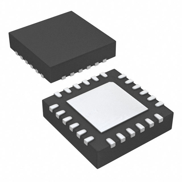


 工商网监
湘ICP备2023018690号
工商网监
湘ICP备2023018690号
