Si5365
P I N - P ROGRAMMABLE P R E C I S I O N C LOCK M U LT IP L I E R
Features
Not recommended for new
designs. For alternatives, see the
Si533x family of products.
Selectable output frequencies
ranging from 19.44 to 1050 MHz
Low jitter clock outputs w/jitter
generation as low as 0.6 ps rms
(50 kHz–80 MHz)
Integrated loop filter with
selectable loop bandwidth
(150 kHz to 1.3 MHz)
Four clock inputs w/manual or
automatically controlled
switching
Five clock outputs with selectable
signal format (LVPECL, LVDS,
CML, CMOS)
Support for ITU G.709 FEC ratios
(255/238, 255/237, 255/236)
LOS alarm outputs
Pin-programmable settings
On-chip voltage regulator for
1.8 ±5%, 2.5 V ±10%, or
3.3 V ±10% operation
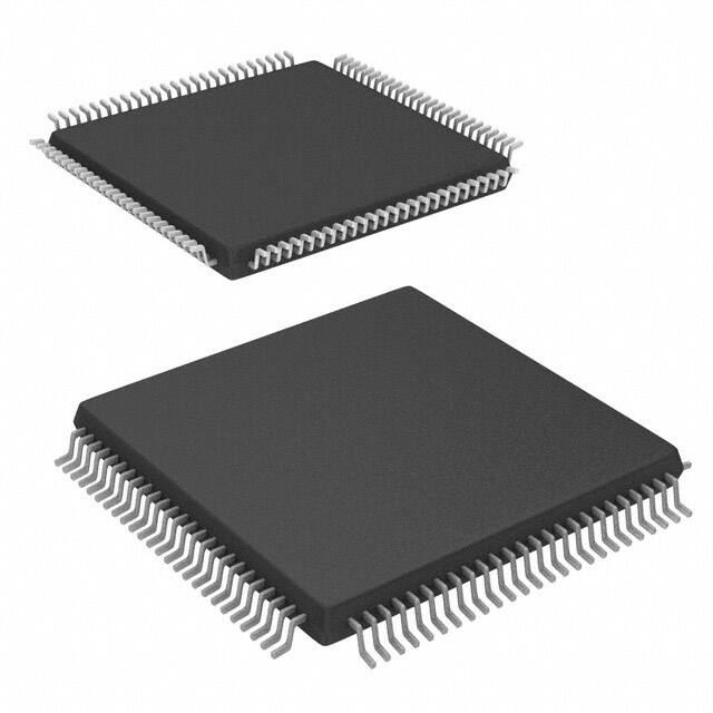
Small size: 14 x 14 mm 100-pin
TQFP
Pb-free, RoHS compliant
Ordering Information:
See page 21.
Applications
SONET/SDH OC-48/STM-16
ITU G.709 line cards
and STM-64/OC-192 line cards Test and measurement
GbE/10GbE, 1/2/4/8/10GFC line
cards
Description
The Si5365 is a low-jitter, precision clock multiplier for high-speed
communication systems, including SONET OC-48/OC-192, Ethernet, and
Fibre Channel, in which the application requires clock multiplication
without jitter attenuation. The Si5365 accepts four clock inputs ranging
from 19.44 to 707 MHz and generates five frequency-multiplied clock
outputs ranging from 19.44 to 1050 MHz. The input clock frequency and
clock multiplication ratio are selectable from a table of popular SONET,
Ethernet, and Fibre Channel frequencies. The Si5365 is based on Silicon
Laboratories' 3rd-generation DSPLL® technology, which provides anyfrequency synthesis in a highly integrated PLL solution that eliminates the
need for external VCXO and loop filter components. The DSPLL loop
bandwidth is digitally programmable, providing jitter performance
optimization at the application level. Operating from a single 1.8, 2.5, or
3.3 V supply, the Si5365 is ideal for providing clock multiplication in high
performance timing applications.
Rev. 1.0 9/14
Copyright © 2014 by Silicon Laboratories
Si5365
�Si5365
Functional Block Diagram
CKIN1
÷ N31
CKIN2
÷ N32
CKIN3
÷ N33
CKIN4
÷ N34
÷ NC1
CKOUT1
÷ NC2
CKOUT2
÷ NC3
CKOUT3
DSPLL®
÷ N2
Divider Select
Manual/Auto Switch
÷ NC4
CKOUT4
÷ NC5
CKOUT5
Clock Select
LOS/FOS Alarms
Control
Frequency Select
Bandwidth Select
VDD (1.8, 2.5, or 3.3 V)
GND
2
Rev. 1.0
�Si5365
TABLE O F C ONTENTS
Section
Page
1. Electrical Specifications . . . . . . . . . . . . . . . . . . . . . . . . . . . . . . . . . . . . . . . . . . . . . . . . . . .4
2. Typical Application Schematic . . . . . . . . . . . . . . . . . . . . . . . . . . . . . . . . . . . . . . . . . . . . . 12
3. Functional Description . . . . . . . . . . . . . . . . . . . . . . . . . . . . . . . . . . . . . . . . . . . . . . . . . . . 13
3.1. Further Documentation . . . . . . . . . . . . . . . . . . . . . . . . . . . . . . . . . . . . . . . . . . . . . . . 13
4. Pin Descriptions: Si5365 . . . . . . . . . . . . . . . . . . . . . . . . . . . . . . . . . . . . . . . . . . . . . . . . . .14
5. Ordering Guide . . . . . . . . . . . . . . . . . . . . . . . . . . . . . . . . . . . . . . . . . . . . . . . . . . . . . . . . . . 21
6. Package Outline: 100-Pin TQFP . . . . . . . . . . . . . . . . . . . . . . . . . . . . . . . . . . . . . . . . . . . . 22
7. PCB Land Pattern . . . . . . . . . . . . . . . . . . . . . . . . . . . . . . . . . . . . . . . . . . . . . . . . . . . . . . . .23
8. Top Marking . . . . . . . . . . . . . . . . . . . . . . . . . . . . . . . . . . . . . . . . . . . . . . . . . . . . . . . . . . . . 25
8.1. Si5365 Top Marking . . . . . . . . . . . . . . . . . . . . . . . . . . . . . . . . . . . . . . . . . . . . . . . . . 25
8.2. Top Marking Explanation . . . . . . . . . . . . . . . . . . . . . . . . . . . . . . . . . . . . . . . . . . . . .25
Document Change List . . . . . . . . . . . . . . . . . . . . . . . . . . . . . . . . . . . . . . . . . . . . . . . . . . . . .26
Contact Information . . . . . . . . . . . . . . . . . . . . . . . . . . . . . . . . . . . . . . . . . . . . . . . . . . . . . . . .28
Rev. 1.0
3
�Si5365
1. Electrical Specifications
Table 1. DC Characteristics
(VDD = 1.8 ± 5%, 2.5 ±10%, or 3.3 V ±10%, TA = –40 to 85 °C)
Parameter
Symbol
Test Condition
Min
Typ
Max
Unit
IDD
LVPECL Format
622.08 MHz Out
All CKOUTs Enabled
—
394
435
mA
LVPECL Format
622.08 MHz Out
1 CKOUT Enabled
—
253
294
mA
CMOS Format
19.44 MHz Out
All CKOUTs Enabled
—
278
321
mA
CMOS Format
19.44 MHz Out
1 CKOUT Enabled
—
229
261
mA
Disable Mode
—
165
—
mA
1.8 V ± 5%
0.9
—
1.4
V
2.5 V ± 10%
1
—
1.7
V
3.3 V ± 10%
1.1
—
1.95
V
CKNRIN
Single-ended
20
40
60
kΩ
Single-Ended Input
Voltage Swing
(See Absolute Specs)
VISE
fCKIN < 212.5 MHz
See Figure 1.
0.2
—
—
VPP
fCKIN > 212.5 MHz
See Figure 1.
0.25
—
—
VPP
Differential Input
Voltage Swing
(See Absolute Specs)
VID
fCKIN < 212.5 MHz
See Figure 1.
0.2
—
—
VPP
fCKIN > 212.5 MHz
See Figure 1.
0.25
—
—
VPP
Supply Current1
CKINn Input Pins2
Input Common Mode
Voltage (Input Threshold Voltage)
Input Resistance
VICM
Notes:
1. Current draw is independent of supply voltage
2. No under- or overshoot is allowed.
3. LVPECL outputs require nominal VDD ≥ 2.5 V.
4. This is the amount of leakage that the 3-Level inputs can tolerate from an external driver. See Si53xx Family Reference
Manual for more details.
5. LVPECL, CML, LVDS and low-swing LVDS measured with Fo = 622.08 MHz.
4
Rev. 1.0
�Si5365
Table 1. DC Characteristics (Continued)
(VDD = 1.8 ± 5%, 2.5 ±10%, or 3.3 V ±10%, TA = –40 to 85 °C)
Parameter
Symbol
Test Condition
Min
Typ
Max
Unit
CKOVCM
LVPECL 100 load lineto-line
VDD –
1.42
—
VDD –1.25
V
Differential Output
Swing
CKOVD
LVPECL 100 load lineto-line
1.1
—
1.9
VPP
Single Ended Output
Swing
CKOVSE
LVPECL 100 load lineto-line
0.5
—
0.93
VPP
Differential Output
Voltage
CKOVD
CML 100 load line-toline
350
425
500
mVPP
CKOVCM
CML 100 load line-toline
—
VDD-0.36
—
V
CKOVD
LVDS
100 load line-to-line
500
700
900
mVPP
Low Swing LVDS
100 load line-to-line
350
425
500
mVPP
CKOVCM
LVDS 100 load line-toline
1.125
1.2
1.275
V
CKORD
CML, LVPECL, LVDS
—
200
—
Output Voltage Low
CKOVOLLH
CMOS
—
—
0.4
V
Output Voltage High
CKOVOHLH
VDD = 1.71 V
CMOS
0.8 x
VDD
—
—
V
CKOIO
VDD = 1.8 V
—
7.5
—
mA
VDD = 3.3 V
—
32
—
mA
Output Clocks (CKOUTn)3
Common Mode
Common Mode Output
Voltage
Differential Output
Voltage
Common Mode Output
Voltage
Differential Output
Resistance
Output Drive Current
(CMOS driving into
CKOVOL for output low
or CKOVOH for output
high. CKOUT+ and
CKOUT– shorted
externally)
Notes:
1. Current draw is independent of supply voltage
2. No under- or overshoot is allowed.
3. LVPECL outputs require nominal VDD ≥ 2.5 V.
4. This is the amount of leakage that the 3-Level inputs can tolerate from an external driver. See Si53xx Family Reference
Manual for more details.
5. LVPECL, CML, LVDS and low-swing LVDS measured with Fo = 622.08 MHz.
Rev. 1.0
5
�Si5365
Table 1. DC Characteristics (Continued)
(VDD = 1.8 ± 5%, 2.5 ±10%, or 3.3 V ±10%, TA = –40 to 85 °C)
Parameter
Symbol
Test Condition
Min
Typ
Max
Unit
VDD = 1.71 V
—
—
0.5
V
VDD = 2.25 V
—
—
0.7
V
VDD = 2.97 V
—
—
0.8
V
VDD = 1.89 V
1.4
—
—
V
VDD = 2.25 V
1.8
—
—
V
VDD = 3.63 V
2.5
—
—
V
2-Level LVCMOS Input Pins
Input Voltage Low
Input Voltage High
VIL
VIH
3-Level Input Pins4
Input Voltage Low
VILL
—
—
0.15 x VDD
V
Input Voltage Mid
VIMM
0.45 x
VDD
—
0.55 x VDD
V
Input Voltage High
VIHH
0.85 x
VDD
—
—
V
Input Low Current
IILL
See Note 4
–20
—
—
µA
Input Mid Current
IIMM
See Note 4
–2
—
+2
µA
Input High Current
IIHH
See Note 4
—
—
20
µA
Notes:
1. Current draw is independent of supply voltage
2. No under- or overshoot is allowed.
3. LVPECL outputs require nominal VDD ≥ 2.5 V.
4. This is the amount of leakage that the 3-Level inputs can tolerate from an external driver. See Si53xx Family Reference
Manual for more details.
5. LVPECL, CML, LVDS and low-swing LVDS measured with Fo = 622.08 MHz.
6
Rev. 1.0
�Si5365
Table 1. DC Characteristics (Continued)
(VDD = 1.8 ± 5%, 2.5 ±10%, or 3.3 V ±10%, TA = –40 to 85 °C)
Parameter
Symbol
Test Condition
Min
Typ
Max
Unit
VOL
IO = 2 mA
VDD = 1.71 V
—
—
0.4
V
IO = 2 mA
VDD = 2.97 V
—
—
0.4
V
IO = –2 mA
VDD = 1.71 V
VDD –
0.4
—
—
V
IO = –2 mA
VDD = 2.97 V
VDD –
0.4
—
—
V
RSTb = 0
–100
—
100
µA
LVCMOS Output Pins
Output Voltage Low
Output Voltage Low
Output Voltage High
VOH
Output Voltage High
Disabled Leakage
Current
IOZ
Notes:
1. Current draw is independent of supply voltage
2. No under- or overshoot is allowed.
3. LVPECL outputs require nominal VDD ≥ 2.5 V.
4. This is the amount of leakage that the 3-Level inputs can tolerate from an external driver. See Si53xx Family Reference
Manual for more details.
5. LVPECL, CML, LVDS and low-swing LVDS measured with Fo = 622.08 MHz.
SIGNAL +
Differential I/Os VICM , VOCM
V
VISE , VOSE
SIGNAL –
(SIGNAL +) – (SIGNAL –)
Differential Peak-to-Peak Voltage
VID,VOD
VICM, VOCM
Single-Ended
Peak-to-Peak Voltage
t
SIGNAL +
VID = (SIGNAL+) – (SIGNAL–)
SIGNAL –
Figure 1. Differential Voltage Characteristics
80%
CKIN, CKOUT
20%
tF
tR
Figure 2. Rise/Fall Time Characteristics
Rev. 1.0
7
�Si5365
Table 2. AC Specifications
(VDD = 1.8 ± 5%, 2.5 ±10%, or 3.3 V ±10%, TA = –40 to 85 °C)
Parameter
Symbol
Test Condition
Min
Typ
Max
Unit
19.44
—
707.35
MHz
40
—
60
%
2
—
—
ns
—
—
3
pF
—
—
11
ns
CKINn Input Pins
Input Frequency
CKNF
Input Duty Cycle
(Minimum Pulse
Width)
CKNDC
Input Capacitance
CKNCIN
Input Rise/Fall Time
CKNTRF
Whichever is smaller
(i.e., the 40% / 60%
limitation applies only
to high frequency
clocks)
20–80%
See Figure 2
CKOUTn Output Pins
(See ordering section for speed grade vs frequency limits)
Output Frequency
(Output not configured for CMOS or
Disabled)
CKOF
19.44
—
1050
MHz
Maximum Output
Frequency in CMOS
Format
CKOF
—
—
212.5
MHz
Output Rise/Fall
(20–80 %) @
622.08 MHz output
CKOTRF
Output not configured for
CMOS or Disabled
See Figure 2
—
230
350
ps
Output Rise/Fall
(20–80%) @
212.5 MHz output
CKOTRF
CMOS Output
VDD = 1.71
CLOAD = 5 pF
—
—
8
ns
Output Rise/Fall
(20–80%) @
212.5 MHz output
CKOTRF
CMOS Output
VDD = 2.97
CLOAD = 5 pF
—
—
2
ns
Output Duty Cycle
Uncertainty @
622.08 MHz
CKODC
100 Load
Line-to-Line
Measured at 50% Point
(Not for CMOS)
—
—
+/-40
ps
8
Rev. 1.0
�Si5365
Table 2. AC Specifications (Continued)
(VDD = 1.8 ± 5%, 2.5 ±10%, or 3.3 V ±10%, TA = –40 to 85 °C)
Parameter
Symbol
Test Condition
Min
Typ
Max
Unit
LVCMOS Input Pins
Minimum Reset Pulse
Width
Input Capacitance
tRSTMN
1
Cin
—
—
3
pF
µs
LVCMOS Output Pins
Rise/Fall Times
tRF
CLOAD = 20pf
See Figure 2
—
25
—
ns
LOSTRIG
From last CKINn to
LOS
—
—
750
µs
Output Clock Skew
tSKEW
of CKOUTn to of
CKOUT_m, C
—
—
100
ps
Phase Change due to
Temperature Variation
tTEMP
Max phase changes from
–40 to +85 °C
—
300
500
ps
—
0.05
0.1
dB
Jitter Frequency Loop
Bandwidth
5000/BW
—
—
ns pk-pk
1 kHz Offset
—
–90
—
dBc/Hz
10 kHz Offset
—
–113
—
dBc/Hz
100 kHz Offset
—
–118
—
dBc/Hz
1 MHz Offset
—
–132
—
dBc/Hz
Max spur @ n x f3
(n 1, n x f3 < 100 MHz)
—
–93
–70
dBc
LOSn Trigger Window
Device Skew
PLL Performance
(fin=fout = 622.08 MHz; BW=120 Hz; LVPECL)
Closed Loop Jitter
Peaking
JPK
Jitter Tolerance
JTOL
Phase Noise
fout = 622.08 MHz
CKOPN
Spurious Noise
SPSPUR
Rev. 1.0
9
�Si5365
Table 3. Jitter Generation
Parameter
Symbol
Jitter Gen
OC-192
Test Condition*
Typ
Max
Unit
Measurement Filter
DSPLL
BW2
4–80 MHz
120 Hz
—
.23
—
psrms
0.05–80 MHz
120 Hz
—
.47
—
ps rms
0.12–20 MHz
120 Hz
—
.48
—
ps rms
JGEN
Jitter Gen
OC-48
Min
JGEN
*Note: Test conditions:
1. fIN = fOUT = 622.08 MHz
2.
Clock input: LVPECL
3.
Clock output: LVPECL
4.
PLL bandwidth: 877 kHz
5.
VDD = 3.3 V
6.
TA = 85 °C
Table 4. Thermal Characteristics
(VDD = 1.8 ±5%, 2.5 ±10%, or 3.3 V ±10%, TA = –40 to 85 °C)
Parameter
Thermal Resistance Junction to Ambient
10
Symbol
Test Condition
Value
Unit
JA
Still Air
40
C°/W
Rev. 1.0
�Si5365
Table 5. Absolute Maximum Limits
Symbol
Value
Unit
DC Supply Voltage
VDD
–0.5 to 3.8
V
LVCMOS Input Voltage
VDIG
–0.3 to (VDD + 0.3)
V
CKINn Voltage Level Limits
CKNVIN
0 to VDD
V
XA/XB Voltage Level Limits
XAVIN
0 to 1.2
V
Operating Junction Temperature
TJCT
–55 to 150
C
Storage Temperature Range
TSTG
–55 to 150
C
2
kV
ESD MM Tolerance; All pins except CKIN+/CKIN–
150
V
ESD HBM Tolerance (100 pF, 1.5 kΩ); CKIN+/CKIN–
700
V
ESD MM Tolerance; CKIN+/CKIN–
100
V
Parameter
ESD HBM Tolerance (100 pF, 1.5 kΩ); All pins except
CKIN+/CKIN–
Latch-Up Tolerance
JESD78 Compliant
Note: Permanent device damage may occur if the Absolute Maximum Ratings are exceeded. Functional operation should be
restricted to the conditions as specified in the operation sections of this data sheet. Exposure to absolute maximum
rating conditions for extended periods of time may affect device reliability.
Phase Noise (dBc/Hz)
622 MHz In, 622 MHz Out BW=877 kHz
-50
-70
-90
-110
-130
-150
-170
1000
10000
100000
1000000
10000000 100000000
Offset Frequency (Hz)
Figure 3. Typical Phase Noise Plot
Jitter Bandwidth
RMS Jitter (fs)
OC-48, 12 kHz to 20 MHz
374
OC-192, 20 kHz to 80 MHz
388
OC-192, 4 MHz to 80 MHz
181
OC-192, 50 kHz to 80 MHz
377
Broadband, 800 Hz to 80 MHz
420
Rev. 1.0
11
�Si5365
2. Typical Application Schematic
System
Power
Supply
C10
Ferrite
Bead
1 µF
C1–9
130
VDD
GND
0.1 µF
VDD = 3.3 V
CKOUT1+
130
0.1 µF
+
100
CKIN1+
CKOUT1–
0.1 µF
–
CKIN1–
82
Input
Clock
Sources1
82
Clock
Outputs
VDD = 3.3 V
130
130
CKIN4+
CKIN4–
82
CKOUT5+
0.1 µF
+
100
82
CKOUT5–
0.1 µF
–
Si5365
VDD
Manual/Automatic Clock15 k
Selection (L)
AUTOSEL2
15 k
Input Clock Select
VDD
15 k
Frequency Table Select
VDD
15 k
Frequency Select
Bandwidth Select
15 k
VDD
VDD
15 k
CKOUT_3 and CKOUT_4
Divider Control
Clock Output 2 Disable/15 k
Bypass Mode Control
15 k
VDD
FRQSEL[3:0]2
BWSEL[1:0]2
15 k
15 k
Signal Format Select
FRQTBL2
15 k
VDD
15 k
CKSEL[1:0]3
SFOUT[1:0]2
DIV34[1:0]2
15 k
DBL2_BY2
15 k
Clock Outputs 3 and 4
Disable
CKOUT5 Disable
VDD
15 k
DBL34
DBL52
15 k
Reset
ALRMOUT
RST
CnB
Notes: 1. Assumes differential LVPECL termination (3.3 V) on clock inputs.
2. Denotes tri-level input pins with states designated as L (ground), M (VDD/2), and H (VDD).
3. Assumes manual input clock selection.
Figure 4. Si5365 Typical Application Circuit
12
Rev. 1.0
Alarm Output Indicator
CKIN_n Invalid
Indicator (n = 1 to 3)
�Si5365
3. Functional Description
3.1. Further Documentation
The Si5365 is a low jitter, precision clock multiplier for
high-speed communication systems, including SONET
OC-48/OC-192, SDH STM-16/STM-64, Ethernet, and
Fibre Channel, in which the application requires clock
multiplication without jitter attenuation. The Si5365
accepts four clock inputs ranging from 19.44 to
707 MHz and generates five frequency-multiplied clock
outputs ranging from 19.44 to 1050 MHz. By default the
four clock inputs are at the same frequency and the five
clock outputs are at the same frequency. Two of the
output clocks can be divided down further to generate
an integer sub-multiple frequency. The input clock
frequency and clock multiplication ratio are selectable
from a table of popular SONET, Ethernet, and Fibre
Channel frequencies. In addition to providing clock
multiplication in SONET and datacom applications, the
Si5365
supports
SONET-to-datacom
frequency
translations. Silicon Laboratories offers a PC-based
software utility, DSPLLsim, that can be used to look up
valid Si5365 frequency translations. This utility can be
downloaded from http://www.silabs.com/timing (click on
Documentation).
Consult the Silicon Laboratories Any-Frequency
Precision Clock Family Reference Manual (FRM) for
detailed information about the Si5365. Additional design
support is available from Silicon Laboratories through
your distributor.
Silicon Laboratories has developed a PC-based
software utility called DSPLLsim to simplify device
configuration, including frequency planning and loop
bandwidth selection. The FRM and this utility can be
downloaded from http://www.silabs.com/timing; click on
Documentation.
The Si5365 is based on Silicon Laboratories' 3rdgeneration DSPLL® technology, which provides anyfrequency synthesis in a highly integrated PLL solution
that eliminates the need for external VCXO and loop
filter components. The Si5365 PLL loop bandwidth is
digitally programmable via the BWSEL[1:0] pins and
supports a range from 150 kHz to 1.3 MHz. The
DSPLLsim software utility can be used to calculate valid
loop bandwidth settings for a given input clock
frequency/clock multiplication ratio.
The Si5365 monitors all input clocks for loss-of-signal
and provides a LOS alarm when it detects a missing
clock.
In the case when the input clocks enter alarm
conditions, the PLL will freeze the DCO output
frequency near its last value to maintain operation with
an internal state close to the last valid operating state.
The Si5365 has five differential clock outputs. The
signal format of the clock outputs is programmable to
support LVPECL, LVDS, CML, or CMOS loads. If not
required, unused clock outputs can be powered down to
minimize power consumption. For system-level
debugging, a bypass mode is available which drives the
output clock directly from the input clock, bypassing the
internal DSPLL. The device is powered by a single 1.8,
2.5, or 3.3 V supply.
Rev. 1.0
13
�Si5365
VDD
VDD
CKOUT4+
CKOUT4–
VDD
SFOUT0
VDD
CKOUT2–
CKOUT2+
VDD
NC
VDD
CKOUT5+
CKOUT5–
VDD
DSBL34
VDD
CKOUT1+
CKOUT1–
VDD
SFOUT1
VDD
CKOUT3–
CKOUT3+
VDD
4. Pin Descriptions: Si5365
100 99 98 97 96 95 94 93 92 91 90 89 88 87 86 85 84 83 82 81 80 79 78 77 76
75
1
74
2
3
73
4
5
6
7
72
71
8
68
67
70
69
9
10
11
12
13
14
15
16
17
18
19
20
66
65
Si5365
64
63
62
61
60
59
GND PAD
58
57
56
21
55
22
23
54
53
24
52
51
25
26 27 28 29 30 31 32 33 34 35 36 37 38 39 40 41 42 43 44 45 46 47 48 49 50
GND
VDD
GND
CKIN4+
CKIN4–
GND
VDD
GND
CKIN2+
CKIN2–
GND
DBL2_BY
GND
CKIN3+
CKIN3–
GND
VDD
GND
CKIN1+
CKIN1–
GND
NC
NC
NC
DBL5
NC
NC
RST
FRQTBL
VDD
VDD
GND
GND
C1B
C2B
C3B
ALRMOUT
CS0_C3A
GND
VDD
GND
NC
GND
GND
NC
GND
AUTOSEL
NC
NC
NC
14
Rev. 1.0
NC
NC
NC
NC
FRQSEL3
FRQSEL2
FRQSEL1
FRQSEL0
DIV34_1
DIV34_0
GND
GND
VDD
VDD
BWSEL1
BWSEL0
C2A
C1A
CS1_C4A
FOS_CTL
GND
GND
NC
NC
GND
�Si5365
Table 6. Si5365 Pin Descriptions
Pin #
Pin Name
I/O Signal Level
Description
1, 2, 17,
20, 23,
24, 25,
47, 48,
49, 52,
53, 72,
73, 74,
75, 90
NC
3
RST
I
LVCMOS
4
FRQTBL
I
3-Level
Frequency Table Select.
This pin selects SONET/SDH, datacom, or SONET/SDH to datacom
frequency translation table.
L = SONET/SDH.
M = Datacom.
H = SONET/SDH to Datacom.
This pin has a weak pullup and weak pulldown and defaults to M.
Some designs may require an external resistor voltage divider when
driven by an active device that will tri-state.
5, 6, 15,
27, 32,
42, 62,
63, 76,
79, 81,
84, 86,
89, 91,
94, 96,
99, 100
VDD
VDD
Supply
VDD.
The device operates from a 1.8 or 2.5 V supply. Bypass capacitors
should be associated with the following VDD pins:
Pins
Bypass Cap
5, 6
0.1 µF
15
0.1 µF
27
0.1 µF
62, 63
0.1 µF
76, 79
1.0 µF
81, 84
0.1 µF
86, 89
0.1 µF
91, 94
0.1 µF
96, 99, 100
0.1 µF
7, 8, 14,
16, 18,
19, 21,
26, 28,
31, 33,
36, 38,
41, 43,
46, 51,
54, 55,
56, 64,
65
GND
GND
Supply
Ground.
These pins must be connected to system ground. Minimize the ground
path impedance for optimal performance.
No Connect.
These pins must be left unconnected for normal operation.
External Reset.
Active low input that performs external hardware reset of device.
Resets all internal logic to a known state and forces the device registers
to their default value. Clock outputs are tristated during reset. After rising edge of RST signal, the device will perform an internal self-calibration.
This pin has a weak pullup.
Rev. 1.0
15
�Si5365
Table 6. Si5365 Pin Descriptions (Continued)
Pin #
Pin Name
I/O Signal Level
Description
9
C1B
O
LVCMOS
CKIN1 Invalid Indicator.
This pin is an active high alarm output associated with CKIN1. Once
triggered, the alarm will remain high until CKIN1 is validated.
0 = No alarm on CKIN1.
1 = Alarm on CKIN1.
10
C2B
O
LVCMOS
CKIN2 Invalid Indicator.
This pin is an active high alarm output associated with CKIN2. Once
triggered, the alarm will remain high until CKIN2 is validated.
0 = No alarm on CKIN2.
1 = Alarm on CKIN2.
11
C3B
O
LVCMOS
CKIN3 Invalid Indicator.
This pin is an active high alarm output associated with CKIN3.
0 = No alarm on CKIN3.
1 = Alarm on CKIN3.
12
ALRMOUT
O
LVCMOS
Alarm Output Indicator.
This pin is an active high alarm output associated with CKIN4 or the
frame sync alignment alarm.
0 = ALRMOUT not active.
1 = ALRMOUT active.
13
57
CS0_C3A
CS1_C4A
I/O
LVCMOS
Input Clock Select/CKINn Active Clock Indicator.
Input: If manual clock selection mode is chosen (AUTOSEL = 1), the
CS[1:0] pins function as the manual input clock selector control.
CS[1:0]
Active Input Clock
00
CKIN1
01
CKIN2
10
CKIN3
11
CKIN4
These inputs are internally deglitched to prevent inadvertent
clock switching during changes in the CSn input state. If configured as input, these pins must not float.
Output: If automatic clock detection is chosen (AUTOSEL = M or H),
these pins function as the CKINn active clock indicator output.
0 = CKINn is not the active input clock.
1 = CKINn is currently the active input clock to the PLL.
This pin has a weak pulldown.
16
22
AUTOSEL
I
3-Level
Manual/Automatic Clock Selection.
Three level input that selects the method of input clock selection to be
used.
L = Manual.
M = Automatic non-revertive.
H = Automatic revertive.
This pin has a weak pullup and weak pulldown and defaults to M.
Some designs may require an external resistor voltage divider when
driven by an active device that will tri-state.
29
30
CKIN4+
CKIN4–
I
MULTI
Clock Input 4.
Differential clock input. This input can also be driven with a singleended signal.
Rev. 1.0
�Si5365
Table 6. Si5365 Pin Descriptions (Continued)
Pin #
Pin Name
I/O Signal Level
Description
34
35
CKIN2+
CKIN2–
I
MULTI
Clock Input 2.
Differential input clock. This input can also be driven with a singleended signal.
37
DBL2_BY
I
3-Level
CKOUT2 Disable/PLL Bypass Mode Control.
Controls enable of CKOUT2 divider/output buffer path and PLL bypass
mode.
L = CKOUT2 Enabled.
M = CKOUT2 Disabled.
H = BYPASS Mode with CKOUT2 enabled. Bypass is not available with
CMOS outputs.
This pin has a weak pullup and weak pulldown and defaults to M.
Some designs may require an external resistor voltage divider when
driven by an active device that will tri-state.
39
40
CKIN3+
CKIN3–
I
MULTI
Clock Input 3.
Differential clock input. This input can also be driven with a singleended signal.
44
45
CKIN1+
CKIN1–
I
MULTI
Clock Input 1.
Differential clock input. This input can also be driven with a singleended signal.
50
DBL5
I
3-Level
CKOUT5 Disable.
This pin performs the following functions:
L = Normal operation. Output path is active and signal format is determined by SFOUT inputs.
M = CMOS signal format. Overrides SFOUT signal format to allow
CKOUT5 to operate in CMOS format while the clock outputs operate in
a differential output format.
H = Powerdown. Entire CKOUT5 divider and output buffer path is powered down. CKOUT5 output will be in tristate mode during powerdown.
This pin has a weak pullup and weak pulldown and defaults to M.
Some designs may require an external resistor voltage divider when
driven by an active device that will tri-state.
56
FOS_CTL
I
3-Level
Frequency Offset Control.
This pin enables or disables use of the CKIN2 FOS reference as an
input to the clock selection state machine.
L = FOS Disabled.
M = Stratum 3/3E FOS Threshold.
H = SONET Minimum Clock FOS Threshold.
This pin has both weak pullups and weak pulldowns and defaults to M.
Some designs may require an external resistor voltage divider when
driven by an active device that will tri-state.
58
C1A
O
LVCMOS
CKIN1 Active Clock Indicator.
This pin serves as the CKIN1 active clock indicator.
0 = CKIN1 is not the active input clock.
1 = CKIN1 is currently the active input clock to the PLL.
59
C2A
O
LVCMOS
CKIN2 Active Clock Indicator.
This pin serves as the CKIN2 active clock indicator.
0 = CKIN2 is not the active input clock.
1 = CKIN2 is currently the active input clock to the PLL.
Rev. 1.0
17
�Si5365
Table 6. Si5365 Pin Descriptions (Continued)
Pin #
Pin Name
60
61
BWSEL0
BWSEL1
I
3-Level
Bandwidth Select.
These pins are three level inputs that select the DSPLL closed loop
bandwidth according to the Any-Frequency Precision Clock Family Reference Manual.
These pins have both weak pullups and weak pulldowns and default to
M.
Some designs may require an external resistor voltage divider when
driven by an active device that will tri-state.
66
67
DIV34_0
DIV34_1
I
3-Level
CKOUT3 and CKOUT4 Divider Control.
These pins control the division of CKOUT3 and CKOUT4 relative to the
CKOUT2 output frequency. Detailed operations and timing characteristics for these pins may be found in the Any-Frequency Precision Clock
Family Reference Manual.
These pins have both weak pullups and weak pulldowns and default to
M.
Some designs may require an external resistor voltage divider when
driven by an active device that will tri-state.
68
69
70
71
FRQSEL0
FRQSEL1
FRQSEL2
FRQSEL3
I
3-Level
Multiplier Select.
These pins are three level inputs that select the input clock and clock
multiplication setting according to the Any-Frequency Precision Clock
Family Reference Manual, depending on the FRQTBL setting.
These pins have both weak pullups and weak pulldowns and default to
M.
Some designs may require an external resistor voltage divider when
driven by an active device that will tri-state.
77
78
CKOUT3+
CKOUT3–
O
MULTI
Clock Output 3.
Differential output clock with a frequency specified by FRQSEL and
FRQTBL settings. Output is differential for LVPECL, LVDS, and CML
compatible modes. For CMOS format, both output pins drive identical
single-ended clock outputs.
18
I/O Signal Level
Description
Rev. 1.0
�Si5365
Table 6. Si5365 Pin Descriptions (Continued)
Pin #
Pin Name
80
95
SFOUT1
SFOUT0
I/O Signal Level
I
3-Level
Description
Signal Format Select.
Three level inputs that select the output signal format (common mode
voltage and differential swing) for all of the clock outputs except
CKOUT5 (see DBL5).
SFOUT[1:0]
Signal Format
HH
Reserved
HM
LVDS
HL
CML
MH
LVPECL
MM
Reserved
ML
LVDS—Low Swing
LH
CMOS
LM
Disable
LL
Reserved
Bypass mode is not available with CMOS outputs. When VDD = 3.3 V,
for thermal reasons, there are restrictions on the number of LVPECL
and CMOS outputs. See the Si53xx-RM reference manual for details.
These pins have both weak pullups and weak pulldowns and default to
M.
Some designs may require an external resistor voltage divider when
driven by an active device that will tri-state.
82
83
CKOUT1–
CKOUT1+
O
MULTI
85
DBL34
I
LVCMOS
87
88
CKOUT5–
CKOUT5+
O
MULTI
Clock Output 5.
Fifth high-speed clock output with a frequency specified by FRQSEL
and FRQTBL. Output signal format is selected by SFOUT pins. Output
is differential for LVPECL, LVDS, and CML compatible modes. For
CMOS format, both output pins drive identical single-ended clock outputs.
92
93
CKOUT2+
CKOUT2–
O
MULTI
Clock Output 2.
Differential output clock with a frequency specified by FRQSEL and
FRQTBL. Output signal format is selected by SFOUT pins. Output is
differential for LVPECL, LVDS, and CML compatible modes. For CMOS
format, both output pins drive identical single-ended clock outputs.
Clock Output 1.
Differential output clock with a frequency specified by FRQSEL and
FRQTBL. Output signal format is selected by SFOUT pins. Output is
differential for LVPECL, LVDS, and CML compatible modes. For CMOS
format, both output pins drive identical single-ended clock outputs.
Output 3 and 4 Disable.
Active high input. When active, entire CKOUT3 and CKOUT4 divider
and output buffer path is powered down. CKOUT3 and CKOUT4 outputs will be in tristate mode during powerdown.
This pin has a weak pullup.
Rev. 1.0
19
�Si5365
Table 6. Si5365 Pin Descriptions (Continued)
Pin #
Pin Name
I/O Signal Level
97
98
CKOUT4–
CKOUT4+
O
GND
PAD
20
GND PAD GND
Description
MULTI
Clock Output 4.
Differential output clock with a frequency specified by FRQSEL and
FRQTBL settings. Output signal format is selected by SFOUT pins.
Output is differential for LVPECL, LVDS, and CML compatible modes.
For CMOS format, both output pins drive identical single-ended clock
outputs.
Supply
Ground Pad.
The ground pad must provide a low thermal and electrical impedance to
a ground plane.
Rev. 1.0
�Si5365
5. Ordering Guide
Ordering Part Number
Package
ROHS6, Pb-Free
Temperature Range
Si5365-C-GQ*
100-Pin 14 x 14 mm TQFP
Yes
–40 to 85 °C
*Note: Not recommended for new designs. For alternatives, see the Si533x family.
Rev. 1.0
21
�Si5365
6. Package Outline: 100-Pin TQFP
Figure 5 illustrates the package details for the Si5365. Table 7 lists the values for the dimensions shown in the
illustration.
Figure 5. 100-Pin Thin Quad Flat Package (TQFP)
Table 7. 100-Pin Package Diagram Dimensions
Dimension
Min
Nom
Max
Dimension
Min
Nom
A
—
—
1.20
E
16.00 BSC.
A1
0.05
—
0.15
E1
14.00 BSC.
A2
0.95
1.00
1.05
E2
3.85
4.00
4.15
b
0.17
0.22
0.27
L
0.45
0.60
0.75
c
0.09
—
0.20
aaa
—
—
0.20
D
16.00 BSC.
bbb
—
—
0.20
D1
14.00 BSC.
ccc
—
—
0.08
ddd
—
—
0.08
0º
3.5º
7º
D2
e
3.85
4.00
4.15
0.50 BSC.
Notes:
1. All dimensions shown are in millimeters (mm) unless otherwise noted.
2. Dimensioning and Tolerancing per ANSI Y14.5M-1994.
3. This package outline conforms to JEDEC MS-026, variant AED-HD.
4. Recommended card reflow profile is per the JEDEC/IPC J-STD-020C specification for Small Body
Components.
22
Max
Rev. 1.0
�Si5365
7. PCB Land Pattern
Figure 6. PCB Land Pattern Diagram
Rev. 1.0
23
�Si5365
Table 8. PCB Land Pattern Dimensions
Dimension
MIN
MAX
e
0.50 BSC.
E
15.40 REF.
D
15.40 REF.
E2
3.90
4.10
D2
3.90
4.10
GE
13.90
—
GD
13.90
—
X
—
0.30
Y
1.50 REF.
ZE
—
16.90
ZD
—
16.90
R1
R2
0.15 REF
—
1.00
Notes:
General
1. All dimensions shown are in millimeters (mm) unless otherwise noted.
2. Dimensioning and Tolerancing is per the ANSI Y14.5M-1994 specification.
3. This Land Pattern Design is based on IPC-7351 guidelines.
4. All dimensions shown are at Maximum Material Condition (MMC). Least Material Condition
(LMC) is calculated based on a Fabrication Allowance of 0.05 mm.
Solder Mask Design
5. All metal pads are to be non-solder mask defined (NSMD). Clearance between the solder
mask and the metal pad is to be 60 µm minimum, all the way around the pad.
Stencil Design
6. A stainless steel, laser-cut and electro-polished stencil with trapezoidal walls should be
used to assure good solder paste release.
7. The stencil thickness should be 0.125 mm (5 mils).
8. The ratio of stencil aperture to land pad size should be 1:1 for the perimeter pads.
9. A 4 x 4 array of 0.80 mm square openings on 1.05 mm pitch should be used for the center
ground pad.
Card Assembly
10. A No-Clean, Type-3 solder paste is recommended.
11. The recommended card reflow profile is per the JEDEC/IPC J-STD-020C specification for
Small Body Components.
24
Rev. 1.0
�Si5365
8. Top Marking
8.1. Si5365 Top Marking
8.2. Top Marking Explanation
Mark Method:
Laser
Logo Size:
9.2 x 3.1 mm
Center-Justified
Font Size:
3.0 Point (1.07 mm)
Right-Justified
Line 1 Marking:
Device Part Number
Si5365x-C-GQ
X = Speed Grade
See "5. Ordering Guide" on page 21.
Line 2 Marking:
YY = Year
WW = Workweek
Assigned by the Assembly Supplier.
Corresponds to the year and workweek of the mold date.
R = Die Revision
Line 3 Marking:
TTTTT = Mfg Code
Manufacturing Code
Circle = 1.8 mm Diameter
Center-Justified
“e3” Pb-Free Symbol
Country of Origin
ISO Code Abbreviation
Rev. 1.0
25
�Si5365
DOCUMENT CHANGE LIST
Revision 0.32 to Revision 0.33
Condensed format.
Revision 0.33 to Revision 0.34
Removed references to latency control, INC, and
DEC pins.
Updated Table 1, “Performance Specifications,” on
page 2.
Changed LVTTL to LVCMOS in Table 2, “Absolute
Maximum Ratings,” on page 3.
Added Figure 1, “Typical Phase Noise Plot,” on page
4.
Updated Figure 4, “Si5365 Typical Application
Circuit”.
Updated “4. Pin Descriptions: Si5365”.
Updated "5. Ordering Guide" on page 21.
Added “7. PCB Land Pattern”.
Revision 0.34 to Revision 0.4
Changed 1.8 V operating range to ±5%.
Updated Table 1 on page 2.
Updated Table 2 on page 3.
Added page 4.
Updated "3. Functional Description" on page 13.
Clarified "4. Pin Descriptions: Si5365" on page 14
including the addition of FOS_CTL (pin 56).
Revision 0.4 to Revision 0.5
Changed “rate” to “frequency” throughout.
Added Table of Contents.
Reordered and expanded spec tables.
Added 3.3 V operation.
Added "8. Top Marking" on page 25.
Added no bypass with CMOS outputs.
Updated Table 2, “AC Specifications,” on page 8.
Updated Table 3, “Jitter Generation,” on page 10.
Updated "5. Ordering Guide" on page 21.
Revision 0.5 to Revision 1.0
Updated logo.
Transitioned to full production.
26
Rev. 1.0
�Si5365
NOTES:
Rev. 1.0
27
�ClockBuilder Pro
One-click access to Timing tools,
documentation, software, source
code libraries & more. Available for
Windows and iOS (CBGo only).
www.silabs.com/CBPro
Timing Portfolio
www.silabs.com/timing
SW/HW
www.silabs.com/CBPro
Quality
www.silabs.com/quality
Support and Community
community.silabs.com
Disclaimer
Silicon Laboratories intends to provide customers with the latest, accurate, and in-depth documentation of all peripherals and modules available for system and software implementers using
or intending to use the Silicon Laboratories products. Characterization data, available modules and peripherals, memory sizes and memory addresses refer to each specific device, and
"Typical" parameters provided can and do vary in different applications. Application examples described herein are for illustrative purposes only. Silicon Laboratories reserves the right to
make changes without further notice and limitation to product information, specifications, and descriptions herein, and does not give warranties as to the accuracy or completeness of the
included information. Silicon Laboratories shall have no liability for the consequences of use of the information supplied herein. This document does not imply or express copyright licenses
granted hereunder to design or fabricate any integrated circuits. The products are not designed or authorized to be used within any Life Support System without the specific written consent
of Silicon Laboratories. A "Life Support System" is any product or system intended to support or sustain life and/or health, which, if it fails, can be reasonably expected to result in significant
personal injury or death. Silicon Laboratories products are not designed or authorized for military applications. Silicon Laboratories products shall under no circumstances be used in
weapons of mass destruction including (but not limited to) nuclear, biological or chemical weapons, or missiles capable of delivering such weapons.
Trademark Information
Silicon Laboratories Inc.® , Silicon Laboratories®, Silicon Labs®, SiLabs® and the Silicon Labs logo®, Bluegiga®, Bluegiga Logo®, Clockbuilder®, CMEMS®, DSPLL®, EFM®, EFM32®,
EFR, Ember®, Energy Micro, Energy Micro logo and combinations thereof, "the world’s most energy friendly microcontrollers", Ember®, EZLink®, EZRadio®, EZRadioPRO®, Gecko®,
ISOmodem®, Precision32®, ProSLIC®, Simplicity Studio®, SiPHY®, Telegesis, the Telegesis Logo®, USBXpress® and others are trademarks or registered trademarks of Silicon Laboratories Inc. ARM, CORTEX, Cortex-M3 and THUMB are trademarks or registered trademarks of ARM Holdings. Keil is a registered trademark of ARM Limited. All other products or brand
names mentioned herein are trademarks of their respective holders.
Silicon Laboratories Inc.
400 West Cesar Chavez
Austin, TX 78701
USA
http://www.silabs.com
�


 工商网监
湘ICP备2023018690号
工商网监
湘ICP备2023018690号
