TS1100 Current-Sense Amplifier
Demo Board
FEATURES
RSENSE: 50mΩ ± 1%
Fully Assembled and Tested
2in x 2in 2-layer circuit board
COMPONENT LIST
DESIGNATION
C1
QTY
1
C2
1
R1
U1
1
1
VBATT, VOUT,
LOAD
3
DESCRIPTION
0.1µF ±10%
capacitor (0805)
47nF ±10%
capacitor (0805)
50mΩ ± 1% (0805)
TS1100-25DB/
TS1100-50DB/
TS1100-100DB/
TS1100-200DB
Test points
DESCRIPTION
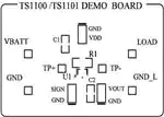
The demo board for the TS1100 is a completely
assembled and tested circuit board that can be used
for evaluating the current-sense amplifier for all (4)
gain options; i.e., 25V/V, 50V/V, 100V/V, and 200V/V.
The board is configured with an RSENSE =R1=50mΩ
resistor. The board has a dedicated RS+=VBATT,
RS-=LOAD, and output voltage OUT=VOUT test
points. For additional information, refer to the TS1100
product datasheet.
All TS1100s are available in a PCB-space saving 5lead SOT23 surface-mount package.
Product data sheets and additional documentation
can be found at www.silabs.com.
ORDERING INFORMATION
Order Number
TS1100-25DB
TS1100-50DB
TS1100-100DB
TS1100-200DB
Description
TS1100-XXX
Demo Board
DESCRIPTION
Figure 1. TS1100 current-sense amplifier circuit
Page 1
© 2014 Silicon Laboratories, Inc. All rights reserved.
�TS1100 Current-Sense Amplifier Demo Board
The demo board includes an on-board 0.1µF
decoupling capacitor at the VBATT input pin and a
47nF capacitor at the VOUT output pin. Depending on
the load current desired, an external resistor or active
load is to be connected to the LOAD pin.
QUICK START PROCEDURE
Required Equipment
TS1100 demo board
A DC Power Supply, an HP Model HP6624A or
equivalent
Two digital voltmeters
Load resistor or an active load (value varies
depending on ILOAD desired)
Signal
Eval board
VBATT
RS+
LOAD
RSVOUT
OUT
GND
GND
Table 1. Demo board test points
MAX
VSENSE
(mV)
25
6
1600 3.75
2
80
50
6
800
7.5
2
40
100
6
400
15
2
20
200
6
200
30
2
10
Table 2. Demo board test set-up per gain setting
VBATT
(V)
ILOAD
(mA)
RLOAD
(Ω)
5) Based on the selected gain option of the current
sense amplifier, select the load resistor or an
active load according to Table 2. Connect one
end of this resistor or active load to the pad
labeled LOAD and the other end to the adjacent
pad labeled GND.
6) Turn on the power supply and observe the output
voltage at VOUT. The expression for the TS1100’s
output voltage is given by:
GAIN
(V/V)
negative terminal to the adjacent test point
labeled GND.
VOUT
(V)
VOUT = ILOAD x 50mΩ x ROUT/R1
where the TS1100’s internal ROUT and R1 resistor
values are listed in Table 3.
GAIN(V/V)
R1 (Ω)
ROUT (Ω)
25
400
10k
50
200
10k
100
100
10k
200
100
20k
Table 3. TS1100’s Internal Gain Setting Resistors
(typical values)
7) The TS1100’s actual output voltage VOUT will
depend on the TS1100’s actual offset voltage
VOS, its gain error GE, sense resistor (RSENSE)
tolerance of ±1%, and the load resistor
tolerance/active load accuracy.
To evaluate the TS1100 current-sense amplifier
circuit, the following steps are to be performed:
1) Before connecting the DC power supply to the
demo board, turn on the power supply, set the
DC voltage to 6V, set its short circuit current limit
to 10% higher than the maximum load current in
the application, and then turn it off.
2) Connect the DC power supply positive terminal to
the pad labeled VBATT and its negative terminal to
the adjacent pad labeled GND.
3) Connect a digital voltmeter to the test points
labeled TP+ and TP- to measure VSENSE.
4) Connect the positive terminal of a second digital
voltmeter to the test point labeled VOUT and the
Page 2 Silicon Laboratories, Inc.
400 West Cesar Chavez, Austin, TX 78701
+1 (512) 416-8500 ▪ www.silabs.com
TS1100-EVB Rev. 1.0
�TS1100 Current-Sense Amplifier Demo Board
Figure 2. Top Layer Component View
Figure 3. Top Layer Component View #2
Figure 4. Bottom Layer (GND)
Figure 5. Bottom Layer (GND) #2
Silicon Laboratories, Inc.
400 West Cesar Chavez, Austin, TX 78701
+1 (512) 416-8500 ▪ www.silabs.com
Page 3
TS1100-EVB Rev. 1.0
�
很抱歉,暂时无法提供与“TS1100-200DB”相匹配的价格&库存,您可以联系我们找货
免费人工找货