TS4100 Demo Board
FEATURES
“Rail-to-Rail PlusTM”, 1% RON Flatness, 0.8V to 5.25V Analog 8-Channel
Switch/Multiplexer
DESCRIPTION
8-Channel Switch/Multiplexer
Low Supply Voltage Operation: 0.8V to 5.25V
On-Resistance of 80Ω
TM
Rail-to-Rail Plus ” input/output voltages can
exceed the supply rails
Fully Assembled and Tested
2in x 2in 4-layer circuit board
COMPONENT LIST
DESIGNATION
QTY
The demo board for the TS4100 is a completely
assembled and tested circuit board that can be used
for
evaluating
the
analog
8-channel
switch/multiplexer. This switch/multiplexer is unique
as it can operate at a supply voltage as low as 0.8V
while accepting an input signal swing above the
TM
supply voltage up to 5.25V (“Rail-to-Rail Plus ”). The
on-resistance variation over the entire signal swing
range is less than 1% exhibiting excellent linearity
and consistency in dynamic and measurement
applications.
DESCRIPTION
C1
1
C2
1
R1-R8
R9
U1
VDD, COM, GND,
0-7
J1, INH, A, B, C
8
1
1
12
10pF ±10% capacitor
(0603)
1µF ±10% capacitor
(0603)
100kΩ ± 1% (0603)
1kΩ ± 1% (0603
TS4100
Test points
5
Jumper
The board is configured for testing all 8 channels,
NO0-NO7, with a DC input voltage derived from VDD.
Jumper INH is available to turn all switches OFF.
Jumper A, B, and C is available to select a channel.
The TS4100 is fully specified over the -40°C to +85°C
temperature range and is available in a low-profile,
thermally-enhanced 16-pin 3x3mm TQFN package
with an exposed back-side paddle. For best
performance, solder exposed back-side paddle to
PCB ground.
Product datasheet and additional documentation can
be
found
on
the
factory web
site
at
www.touchstonesemi.com.
ORDERING INFORMATION
Order Number
TS4100DB
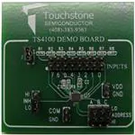
Figure 1. TS4100 Demo Board
(Top View)
Description
TS4100
Demo Board
Figure 2. TS4100 Demo Board
(Bottom View)
Page 1
© 2013 Touchstone Semiconductor, Inc. All rights reserved.
�TS4100 Demo Board
DESCRIPTION
3. Set jumper A, B, and C to a HIGH state by
moving the jumper position from LO to HI.
The TS4100 demo board is configured with a COM
output resistor and capacitor load of 1kΩ and 10pF.
The TS4100 operates at a supply voltage range of
0.8V to 5.25V and an analog input/output “Rail-to-Rail
TM
Plus ” range of 0V to 5.25V.
4. Find the 16-pin header on the board labeled
INPUTS. Place a jumper on the two-pin header
labeled 7. This sets a DC voltage to channel
NO7.
The TS4100 can be tested with an on-board DC input
signal or an external AC input signal. The on-board
voltage is generated via a voltage divider circuit. The
complete demo board circuit is shown in Figure 3. To
select a channel or turn OFF all channels, jumper A,
B, C, and INH can be set according to Table 1.
ADDRESS BITS
COM
Output
A
B
C
X
X
X
GND
1
0
0
0
0
NO0
0
0
0
1
NO1
0
0
1
0
NO2
0
0
1
1
NO3
0
1
0
0
NO4
0
1
0
1
NO5
0
1
1
0
NO6
0
1
1
1
NO7
Table 1: Jumper A, B, C, and INH Setting
INH
QUICK START PROCEDURE
Required Equipment
5. To monitor the COM output signal, connect the
positive terminal of the digital voltmeter to the test
point labeled as COM and the negative terminal
to the adjacent test point labeled as GND.
6. Turn on the power supply and check that the
digital voltmeter is reading an output voltage
of approximately 1.39V. With an output voltage of
1.39V across an output resistor value of 1kΩ, the
resulting load current is 1.39mA. This yields an
on-resistance of approximately 79Ω, which is well
within the datasheet on-resistance specification.
7. To test a different channel, refer to Table 1 and
make the appropriate changes to jumper A, B,
and C.
MEASURING THE SUPPLY CURRENT
8. Turn off the power supply and connect a digital
ammeter in series with the power supply.
9. Remove the positive terminal of the digital
voltmeter from the COM output test point.
10. Remove jumper J1 and the jumper on the
selected channel.
TS4100 Demo Board
DC Power Supply
Digital Ammeter, an HP34410A or equivalent
11. Turn on the power supply and check that the
digital ammeter is reading a supply current less
than 765nA.
Digital Voltmeter, an HP34410A or equivalent
APPLYING AN EXTERNAL INPUT SIGNAL
To evaluate the TS4100 analog 8-channel
switch/multiplexer, the following steps are to be
performed:
1. Before connecting the DC power supply to the
demo board, turn on the power supply, set the
DC voltage to 1.5V, and then turn it off.
2. Connect the DC power supply positive terminal to
the test point labeled VDD. Connect the negative
terminal of the DC power supply to the test point
labeled GND.
TS4100DB r1p0
12. Turn off the power supply.
13. Connect the positive terminal of a DC power
supply or an AC signal generator to the test point
labeled “0” on the 16-pin header labeled
INPUTS. Connect the negative terminal to a test
point labeled GND. For an AC input signal, make
sure the maximum input voltage level is less than
5.25V and the minimum input voltage level is
greater than 0V. For a DC input signal, make
sure the input voltage is less than 5.25V and
greater than 0V.
Page 2
RTFDS
�TS4100 Demo Board
14. Check that the AC input signal levels are within
the levels specified in the previous step with an
oscilloscope. Check a DC input voltage level with
a voltmeter.
17. Turn on the DC power supply input signal or AC
signal generator. For a DC input signal, monitor
the digital voltmeter. For an AC input signal,
monitor the oscilloscope.
15. With an applied DC input signal, connect the
positive terminal of the digital voltmeter to the test
point labeled as COM and the negative terminal
to the adjacent test point labeled as GND. With
an applied AC input signal, connect the signal
terminal of an oscilloscope probe to the test point
labeled as COM and the ground terminal to the
adjacent test point labeled as GND.
TURN OFF ALL SWITCHES
18. Turn off the power supply.
19. Remove the jumper between INH and LO and
connect it between INH and HI. Refer to Table 1.
16. Turn on the power supply.
Figure 3. TS4100 Demo Board Circuit
TS4100DB r1p0
Page 3
RTFDS
�TS4100 Demo Board
Figure 4. Top Layer View #1
Figure 5. Top Layer View #2
Figure 6. Layer 2
Figure 7. Layer 3
Figure 8. Bottom Layer 4 View #1
Figure 9. Bottom Layer 4 View #2
Page 4 Touchstone Semiconductor, Inc.
630 Alder Drive, Milpitas, CA 95035
+1 (408) 215 - 1220 ▪ www.touchstonesemi.com
TS4100DB r1p0
RTFDS
�