WT12
DATA SHEET
Wednesday, 09 April 2014
Version 3.1
�Copyright © 2000-2014 Bluegiga Technologies
All rights reserved.
Bluegiga Technologies assumes no responsibility for any errors which may appear in this manual.
Furthermore, Bluegiga Technologies reserves the right to alter the hardware, software, and/or specifications
detailed here at any time without notice and does not make any commitment to update the information
contained here. Bluegiga’s products are not authorized for use as critical components in life support devices
or systems.
The WRAP is a registered trademark of Bluegiga Technologies
The Bluetooth trademark is owned by the Bluetooth SIG Inc., USA and is licensed to Bluegiga Technologies.
All other trademarks listed herein are owned by their respective owners.
Bluegiga Technologies Oy
�Table of Contents
1
ORDERING INFORMATION .........................................................................................................................6
2
Block Diagram and Descriptions ...................................................................................................................7
3
Electrical Characteristics ...............................................................................................................................9
3.1
Absolute maximum ratings .....................................................................................................................9
3.2
Recommended operating conditions .....................................................................................................9
3.3
Terminal characteristics .........................................................................................................................9
3.4
Current consumption ........................................................................................................................... 10
3.5
Radio characteristics and general specifications ................................................................................ 11
3.6
Radio Characteristics – Basic Data Rate ............................................................................................ 12
3.6.1
Transmitter radio characteristics .................................................................................................. 12
3.6.2
Receiver radio characteristics ...................................................................................................... 13
3.7
Radio Characteristics – Enhanced Data Rate .................................................................................... 15
3.7.1
Transmitter radio characteristics .................................................................................................. 15
3.7.2
Receiver radio characteristics ...................................................................................................... 16
4
WT12 Pin Description ................................................................................................................................. 17
5
Physical Interfaces ..................................................................................................................................... 20
5.1
UART Interface.................................................................................................................................... 20
5.1.1
UART Configuration While RESET is Active ............................................................................... 21
5.1.2
UART Bypass Mode .................................................................................................................... 21
5.2
USB Interface ...................................................................................................................................... 23
5.2.1
USB Pull-Up Resistor ................................................................................................................... 23
5.2.2
Self Powered Mode ...................................................................................................................... 23
5.2.3
Bus Powered Mode ...................................................................................................................... 24
5.2.4
Suspend Current .......................................................................................................................... 24
5.2.5
Detach and Wake-Up Signaling ................................................................................................... 24
5.2.6
USB Driver ................................................................................................................................... 25
5.2.7
USB 1.1 Compliance .................................................................................................................... 25
5.2.8
USB 2.0 Compatibility .................................................................................................................. 25
5.3
SPI Interface........................................................................................................................................ 26
5.4
PCM Interface ..................................................................................................................................... 27
5.4.1
PCM Interface Master/Slave ........................................................................................................ 27
5.4.2
Long Frame Sync ......................................................................................................................... 28
5.4.3
Short Frame Sync ........................................................................................................................ 28
5.4.4
Multi Slot Operation ..................................................................................................................... 29
5.4.5
GCI Interface ................................................................................................................................ 29
5.4.6
Slots and Sample Formats........................................................................................................... 29
5.4.7
Additional Features .................................................................................................................... 30
Bluegiga Technologies Oy
�5.4.8
PCM Configuration ....................................................................................................................... 30
6
I/O Parallel Ports ........................................................................................................................................ 32
7
Software Stacks.......................................................................................................................................... 33
7.1
iWRAP Stack ....................................................................................................................................... 33
7.2
HCI Stack ............................................................................................................................................ 34
7.2.1
Standard functionality .................................................................................................................. 34
7.2.2
Extra functionality: ........................................................................................................................ 36
7.3
VM Stack ............................................................................................................................................. 37
7.4
Software Development ........................................................................................................................ 38
8
Enhanced Data Rate .................................................................................................................................. 39
8.1
Enhanced Data Rate Baseband .......................................................................................................... 39
8.2
...................................................................................................... 39
8.3
8DQPSK .............................................................................................................................................. 39
9
Layout and Soldering Considerations ........................................................................................................ 41
9.1
Soldering recommendations ............................................................................................................... 41
9.2
Layout guidelines ................................................................................................................................ 41
10
WT12 physical dimensions ..................................................................................................................... 44
11
Package .................................................................................................................................................. 46
12
Certifications ........................................................................................................................................... 48
12.1
Bluetooth ...................................................................................................................................... 48
12.2
FCC and IC .................................................................................................................................. 48
12.3
CE ................................................................................................................................................ 50
12.4
Japan ........................................................................................................................................... 50
13
RoHS Statement with a List of Banned Materials ................................................................................... 51
14
Contact Information................................................................................................................................. 52
Bluegiga Technologies Oy
�WT12 Bluetooth module
DESCRIPTION
KEY FEATURES
WT12 is a fully integrated Bluetooth 2.1 +
EDR,
class
2
module
combining
antenna, Bluetooth radio and an on-board
iWRAP Bluetooth stack. Bluegiga WT12
provides an ideal solution for developers that
want to quickly integrate Bluetooth wireless
technology
to
their
design
without
investing several months into Bluetooth radio
and stack development.
Radio features:
WT12
uses
Bluegiga's
iWRAP Bluetooth stack,
which
is
an
embedded Bluetooth stack implementing 13
different Bluetooth profiles and Apple iAP
connectivity. By using WT12 combined with
iWRAP Bluetooth stack
and
Bluegiga's
excellent technical support designers ensure
quick time to market, low development costs
and risk.
APPLICATIONS
Industrial and M2M
Mobile phone and tablet accessories
Point-of-Sale devices
Computer accessories
Apple iOS accessories
Bluetooth v.2.1 + EDR
Bluetooth class 2 radio
Transmit power: +3 dBm
Receiver sensitivity: -86 dBm
Range: 30 meters line-of-sight
Integrated chip antenna
Hardware features:
UART and USB host interfaces
802.11 co-existence interface
6 software programmable IO pins
Opertating voltage: 2.7V to 3.6V
Temperature range: -40C to +85C
Dimensions: 25.5 x 14.0 x 2.4 mm
Qualifications:
Bluetooth
CE
FCC
IC
Japan and South-Korea
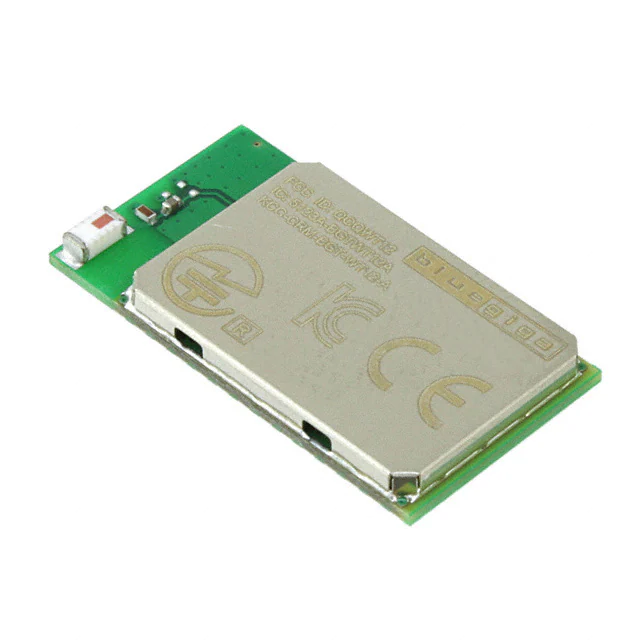
Figure 1: Physical outlook of WT12
Bluegiga Technologies Oy
�1 ORDERING INFORMATION
Internal chip antenna
WT12-A-AI5
WT12-A-AI4
WT12-A-3
WT12-A-HCI21
WT12-A-C (*
iWRAP 5.0 firmware
iWRAP 4.0 firmware
iWRAP 3.0 firmware
HCI firmware, BT2.1 + EDR
Custom firmware
Table 1: Ordering information
*) Custom firmware means any standard firmware with custom parameters (like UART baud rate), custom firmware developer by
customer or custom firmware developed by Bluegiga for the customer.
To order custom firmware you must have a properly filled Custom Firmware Order From and unique ordering code issued by
Bluegiga.
Contact sales@bluegiga.com for more information.
Bluegiga Technologies Oy
�2 Block Diagram and Descriptions
Figure 2: Block Diagram of WT12
BlueCore04
BlueCore4 is a single chip Bluetooth solution which implements the Bluetooth radio transceiver and also
an on chip microcontroller. BlueCore4 implements Bluetooth® 2.1 + EDR (Enhanced Data Rate) and it
can deliver data rates up to 3 Mbps.
The microcontroller (MCU) on BlueCore04 acts as interrupt controller and event timer run the Bluetooth
software stack and control the radio and host interfaces. A 16-bit reduced instruction set computer
(RISC) microcontroller is used for low power consumption and efficient use of memory.
BlueCore04 has 48Kbytes of on-chip RAM is provided to support the RISC MCU and is shared between
the ring buffers used to hold voice/data for each active connection and the general purpose memory
required by the Bluetooth stack.
Crystal
The crystal oscillates at 26MHz.
Flash
Flash memory is used for storing the Bluetooth protocol stack and Virtual Machine applications. It can
also be used as an optional external RAM for memory intensive applications.
Balun / filter
Combined balun and filter changes the balanced input/output signal of the module to unbalanced signal
of the monopole antenna. The filter is a band pass filter (ISM band).
Matching
Antenna matching components match the antenna to 50 Ohms.
Bluegiga Technologies Oy
�Antenna
The antenna is ACX AT3216 chip antenna.
USB
This is a full speed Universal Serial Bus (USB) interface for communicating with other compatible digital
devices. WT12 acts as a USB peripheral, responding to requests from a Master host controller such as
a PC.
Synchronous Serial Interface
This is a synchronous serial port interface (SPI) for interfacing with other digital devices. The SPI port
can be used for system debugging. It can also be used for programming the Flash memory.
UART
This is a standard Universal Asynchronous Receiver Transmitter (UART) interface for communicating
with other serial devices.
Audio PCM Interface
The audio pulse code modulation (PCM) Interface supports continuous transmission and reception of
PCM encoded audio data over Bluetooth.
Programmable I/O
WT12 has a total of 6 digital programmable I/O terminals. These are controlled by firmware running on
the device.
Reset
This can be used to reset WT12.
802.11 Coexistence Interface
Dedicated hardware is provided to implement a variety of coexistence schemes. Channel skipping AFH
(Adaptive Frequency Hopping), priority signaling, channel signaling and host passing of channel
instructions are all supported. The features are configured in firmware. Since the details of some
methods are proprietary (e.g. Intel WCS) please contact Bluegiga Technologies for details.
Bluegiga Technologies Oy
�3 Electrical Characteristics
3.1 Absolute maximum ratings
Min
-40
-40
-0,3
-0,4
Storage temperature
Operating temperature
Supply voltage
Terminal voltages
Output current from PIOS
Max
85
85
3,6
Vdd + 0,4
35
Unit
°C
°C
V
V
mA
The module should not continuously run under these conditions. Exposure to absolute maximum rating conditions for extended periods of
time may affect reliability and cause permanent damage to the device.
Table 2: Absolute maximum ratings
3.2 Recommended operating conditions
Min
-40
3,1 (1)
0
Operating temperature
Supply voltage
Terminal voltages
Max
85
3,6
Vdd
Unit
°C
V
V
1)
WT12 operates as low as 2,7 V supply voltage. However, to safely meet the USB specification for minimum voltage for USB data lines,
minimum of 3,1 V supply is required.
Table 3: Recommended operating conditions
3.3 Terminal characteristics
Min
Typ
Max
Unit
I/O voltage levels
VIL input logic level low
-0,4
-
0,8
V
VIH input logic level high
0,7Vdd
-
Vdd + 0,4
V
VOL output logic level low
-
-
0,2
V
VOH output logic level high
Reset terminal
VTH,res threshold voltage
Vdd - 0,2
-
-
V
0,64
0,85
1,5
RIRES input resistance
220
V
k
CIRES input capacitance
Input and tri-state current with
Strong pull-up
Strong pull-down
Weak pull-up
Weak pull-down
I/O pad leakage current
Vdd supply current
TX mode
RX mode
220
nF
-100
10
-5
0,2
-1
-40
40
-1
1
0
-10
100
-0,2
5
1
-
-
70
70
mA
mA
Table 4: Terminal characteristics
Bluegiga Technologies Oy
�3.4 Current consumption
Test conditions: Room temperature, Vdd = 3,3 V, iWRAP firmware
OPERATION MODE
Peak
AVG
supply supply Unit
current current
Notes
Peak current at TX mode
70
-
mA
-
Peak current at RX mode
IDLE
IDLE, Deep Sleep ON
IDLE, Deep Sleep ON
NOT visible, NOT
connectable
INQUIRY
NAME
CALL
CONNECT
Master
CONNECT
Slave
CONNECT + Sniff, Master
CONNECT + Sniff, Slave
70
-
3
1,2
mA
mA
mA
Module is idle Default settings
Module is idle
-
0,056
mA
Module is idle (Minimum consumption),
SET BT PAGEMODE 0 2000 1
-
44,7
44,7
44,7
mA
mA
mA
Device discovery with INQUIRY command
Name resolution
CALL [ADDR] 1101 RFCOMM
-
6,2
mA
No data was transmitted, Default settings
-
22,4
mA
No data was transmitted, Default settings
-
4,7
4,6
mA
mA
CONNECT + sniff, Master
-
2,3
mA
CONNECT + sniff, Slave
-
2,3
mA
CONNECT + park, Master
CONNECT + park, Slave
DATA, Master
DATA, Slave
-
3,1
2,3
31,5
29,2
mA
mA
mA
mA
DATA + Sniff, Master
-
19,6
mA
DATA + Sniff, Slave
-
22,6
mA
DATA + Sniff, Master
-
3,9
mA
Connected (SET BT SNIFF 40 20 1 8)
Connected (SET BT SNIFF 40 20 1 8)
No data transmitted
(SET BT SNIFF 1000 20 1 8)
No data transmitted
(SET BT SNIFF 1000 20 1 8)
No data transmittedPark parameter 1000
No data transmittedPark parameter 1000
Data transmitted @ 115200bps
Data transmitted @ 115200bps
Data transmitted @ 115200bps
(SET BT SNIFF 40 20 1 8)
Data transmitted @ 115200bps
(SET BT SNIFF 40 20 1 8)
Data transmitted
(SET BT SNIFF 1000 20 1 8)
Table 5: Current consumption
Bluegiga Technologies Oy
�3.5 Radio characteristics and general specifications
Operating
frequency range
Lower quard
band
Upper quard
band
Maximum data
rate
Receiving signal
range
Receiver IF
frequency
Transmission
power
RF input
impedance
Compliance
USB specification
Note
(2400 ... 2483,5) MHz
ISM Band
2 MHz
3,5 MHz
2402 MHz ... 2480 MHz
Carrier frequency
Modulation
method
Hopping
Specification
GFSK (1 Mbps)
P/4 DQPSK (2Mbps)
1600 hops/s, 1 MHz channel space
Asynchronous, 723.2 kbps / 57.6 kbps
GFSK:
Synchronous: 433.9 kbps / 433.9 kbps
P/4
Asynchronous, 1448.5 kbps / 115.2 kbps
DQPSK:
Synchronous: 869.7 kbps / 869.7 kbps
Asynchronous, 2178.1 kbps / 177.2 kbps
8DQPSK:
Synchronous: 1306.9 kbps / 1306.9 kbps
-82 to -20 dBm
1.5 MHz
Min
Max
-11 ... -9 dBm
+1 ... +3 dBm
50
Bluetooth specification, version 2.0 + EDR
USB specification, version 1.1 (USB 2.0 compliant)
Table 6: Radio characteristics and general specifications
Bluegiga Technologies Oy
f = 2402 + k,
k = 0...78
Typical
condition
Center
frequency
�3.6 Radio Characteristics – Basic Data Rate
3.6.1 Transmitter radio characteristics
WT12 meets the Bluetooth v2.1 + EDR specification between -40°C and +85°C. TX output is guaranteed to be unconditionally
stable over the guaranteed temperature range.
Measurement conditions: T = 20C, Vdd = 3,3V
Item
Typical value
Bluetooth specification
Unit
Maximum output power1,2
Variation in RF power over
temperature range with
compensation enabled4
Variation in RF power over
temperature range with
compensation disabled4
RF power control range
RF power range control
resolution5
20dB bandwidth for modulated
carrier
Adjacent channel transmit power
F = F0 ± 2MHz6,7
Adjacent channel transmit power
F = F0 ± 3MHz6,7
Adjacent channel transmit power
F = F0 ± > 3MHz6,7
f1avg Maximum Modulation
+2.5
-6 to 4 3
dBm
1.5
-
dB
2.0
-
dB
35
16
dB
0.5
-
dB
780
1000
kHz
-40
20
dBm
-45
-40
dBm
-50
-40
dBm
165
140


 工商网监
湘ICP备2023018690号
工商网监
湘ICP备2023018690号
