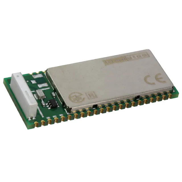
WT41-A / WT41-N
DATA SHEET
Wednesday, 22 January 2014
Version 1.44
�Copyright © 2000-2014 Bluegiga Technologies
All rights reserved.
Bluegiga Technologies assumes no responsibility for any errors which may appear in this manual.
Furthermore, Bluegiga Technologies reserves the right to alter the hardware, software, and/or specifications
detailed here at any time without notice and does not make any commitment to update the information
contained here. Bluegiga’s products are not authorized for use as critical components in life support devices
or systems.
The WRAP is a registered trademark of Bluegiga Technologies
The Bluetooth trademark is owned by the Bluetooth SIG Inc., USA and is licensed to Bluegiga Technologies.
All other trademarks listed herein are owned by their respective owners.
Bluegiga Technologies Oy
�VERSION HISTORY
Version
Comment
0.1
First draft
0.2
Description and product codes added
0.21
Dimensions updated, layout guide added, UART and USB chapters added
0.22
Pin descriptions, PCM, USB, UART, SPI
0.3
Physical dimensions corrected
0.31
Product codes corrected
0.32
Recommendation for a power-up reset circuitry added to chapter 10
0.4
Pins 1 and 52 (GND) removed. Dimensions updated, recommended land
pattern added
0.5
Certification information added
0.6
Physical dimensions and recommended PCB land pattern updated
0.7
Figure 7 recommended land pattern corrected
1.0
Radio and antenna characteristics, layout guide for WT41-N
1.1
Japan certification info added
1.2
FCC RF radiation exposure statement updated
1.3
Layout guide updated
1.31
VDD added to table 1
1.32
FCC and IC statements updated
1.33
PIO current drive capability added. List of approved antennas added.
1.34
IC statements in French added
1.35
Information about Japan compliance updated
1.36
Absolute maximum supply voltage 3.7V
1.37
MIC Japan information updated
Bluegiga Technologies Oy
�1.4
FCC C2PC to remove 20 cm restriction
1.41
MIC Japan ID corrected
1.42
MSL information updated
1.43
TXP vs VDD_PA figure added
1.44
Minor changes
Bluegiga Technologies Oy
�TABLE OF CONTENTS
1
Ordering Information......................................................................................................................................8
2
Pinout and Terminal Description ...................................................................................................................9
3
Electrical Characteristics ............................................................................................................................ 12
3.1
Absolute Maximum Ratings ................................................................................................................ 12
3.2
Recommended Operating Conditions ................................................................................................. 12
3.3
PIO Current Sink and Source Capability ............................................................................................. 12
3.4
Transmitter Performance For BDR ..................................................................................................... 13
3.5
Radiated Spurious Emissions ............................................................................................................. 14
3.6
Receiver Performance ........................................................................................................................ 15
3.7
Current Consumption .......................................................................................................................... 15
3.8
Antenna Performance and Radiation Patterns ................................................................................... 16
4
Physical Dimensions .................................................................................................................................. 20
5
Layout Guidelines ....................................................................................................................................... 22
6
7
5.1
WT41-A ............................................................................................................................................... 22
5.2
WT41-N ............................................................................................................................................... 23
5.2.1
Layout for WT41-N with u.fl connector close to RF pin ............................................................... 23
5.2.2
Layout for WT41-N with 50 ohm trace from RF pin to a SMA connector .................................... 23
UART Interface ........................................................................................................................................... 25
6.1
UART Bypass ...................................................................................................................................... 27
6.2
UART Configuration While Reset is Active ......................................................................................... 27
6.3
UART Bypass Mode ............................................................................................................................ 27
USB Interface ............................................................................................................................................. 28
7.1
USB Data Connections ....................................................................................................................... 28
7.2
USB Pull-Up resistor ........................................................................................................................... 28
7.3
USB Power Supply .............................................................................................................................. 28
7.4
Self-Powered Mode ............................................................................................................................. 28
7.5
Bus-Powered Mode ............................................................................................................................. 29
7.6
USB Suspend Current ......................................................................................................................... 30
7.7
USB Detach and Wake-Up Signaling.................................................................................................. 30
7.8
USB Driver .......................................................................................................................................... 31
7.9
USB v2.0 Compliance and Compatibility ............................................................................................ 31
8
Serial Peripheral Interface (SPI) ................................................................................................................. 32
9
PCM Codec Interface ................................................................................................................................. 33
9.1
PCM Interface Master/Slave ............................................................................................................... 33
9.2
Long Frame Sync ................................................................................................................................ 34
9.3
Short Frame Sync ............................................................................................................................... 34
9.4
Multi-slot Operation ............................................................................................................................. 35
Bluegiga Technologies Oy
�9.5
GCI Interface ....................................................................................................................................... 35
9.6
Slots and Sample Formats .................................................................................................................. 36
9.7
Additional Features ............................................................................................................................. 37
9.8
PCM_CLK and PCM_SYNC Generation ............................................................................................ 37
9.9
PCM Configuration .............................................................................................................................. 38
10
I/O Parallel Ports ..................................................................................................................................... 40
10.1
11
PIO Defaults ................................................................................................................................. 40
Reset ....................................................................................................................................................... 41
11.1
12
Pin States on Reset ..................................................................................................................... 42
Certifications ........................................................................................................................................... 43
12.1
Bluetooth ...................................................................................................................................... 43
12.2
FCC .............................................................................................................................................. 43
12.3
IC (Industry Canada) .................................................................................................................... 44
12.3.1
IC .................................................................................................................................................. 45
12.4
CE ................................................................................................................................................ 47
12.5
Japan ........................................................................................................................................... 47
12.6
Qualified Antenna Types for WT41-N .......................................................................................... 47
12.7
Moisture Sensitivity Level (MSL).................................................................................................. 48
13
Contact Information................................................................................................................................. 49
Bluegiga Technologies Oy
�WT41 Bluetooth® Module
DESCRIPTION
WT41 is a long range class 1, Bluetooth® 2.1 +
EDR module. WT41 is a highly integrated and
sophisticated Bluetooth® module, containing all the
necessary elements from Bluetooth® radio to
antenna and a fully implemented protocol stack.
Therefore WT41 provides an ideal solution for
developers who want to integrate Bluetooth®
wireless technology into their design with limited
knowledge of Bluetooth® and RF technologies.
WT41 is optimized for long range applications and
since it contains a RF power amplifier, low noise
amplifier and a highly efficient chip antenna. With
115 dB radio budget WT41 can reach over 1 km
range in line off sight.
By default WT41 module is equipped with powerful
and easy-to-use iWRAP firmware. iWRAP enables
users to access Bluetooth® functionality with simple
ASCII commands delivered to the module over
serial interface - it's just like a Bluetooth® modem.
FEATURES:
Fully Qualified Bluetooth v2.1 + EDR end
product,
CE, FCC, IC and MIC Japan
TX power : 19 dBm
RX sensitivity : -92 dBm
Higly efficient chip antenna, U.FL connector or
RF pin
Class 1, range up to 800 meters
o
Industrial temperature range from -40 C to
o
+85 C
RoHS Compliant
USB interface (USB 2.0 compatible)
UART with bypass mode
6 x GPIO
1 x 8-bit AIO
Support for 802.11 Coexistence
TM
Integrated iWRAP
Bluetooth stack or HCI
firmware
APPLICATIONS:
Hand held terminals
Industrial devices
Point-of-Sale systems
PCs
Personal Digital Assistants (PDAs)
Computer Accessories
Access Points
Automotive Diagnostics Units
Bluegiga Technologies Oy
�1 Ordering Information
WT41-A-HCI
Firmware
HCI21=
HCI30=
AI4 =
AI5 =
C
=
HCI firmware (Bluetooth 2.1 + EDR)
HCI firmware (Bluetooth 3.0)
iWRAP 4.0.0
iWRAP 5.0.2
Custom*
HW version
A
=
N
=
Chip antenna
RF pin
Product series
Bluegiga Technologies Oy
Page 8 of 49
�Pinout and Terminal Description
59
58
57
56
55
54
53
2
GND
GND
GND
GND
GND
GND
GND
Pins 1 and 52 (GND)
are not connected
and have been
removed
51
RF
RFGND 50
GND
GND
GND
GND
GND
GND
GND
GND
GND
VDD_PA
PIO2
PIO3
UART_RTS
UART_RX
GND
USB+
USBUART_CTS
PCM_IN
PCM_CLK
PCM_SYNC
GND
GND
GND
GND
GND
GND
GND
AIO
UART_TX
PIO5
SPI_MOSI
SPI_MISO
SPI_CLK
SPI_CSB
GND
PIO7
PIO6
RESET
VDD
GND
49
48
47
46
45
44
43
42
41
40
39
38
37
36
35
34
33
32
31
24
25
26
27
28
29
30
GND
PCM_OUT
GND
GND
GND
PIO4
GND
2
3
4
5
6
7
8
9
10
11
12
13
14
15
16
17
18
19
20
21
22
23
Figure 1: WT41 pin out
PIN
NUMBER
NC
RESET
GND
1, 52
33
2-10, 16,
23,24,2628, 30,
31,36,4449, 53-59
PAD TYPE
DESCRIPTION
Pins 1 and 52 (GND) have been removed
from the module.
Input, weak internal pull- Active low reset. Keep low for >5 ms
up
to cause a reset
Not connected
GND
RF
51
RF output
RFGND
50
GND
VDD_PA
11
Supply voltage
VDD
32
Supply voltage
GND
RF output for WT41-N. For WT41-A
and WT41-E this pin is not connected
RF ground. Connected to GND internally to
the module.
Supply voltage for the RF power amplifier
and the low noise amplifier of the module
Supply voltage for BC4 and the flash
memory
Table 1: Supply and RF Terminal Descriptions
Bluegiga Technologies Oy
Page 9 of 49
�PIO PORT
PIN
PAD TYPE
NUMBER
DESCRIPTION
PIO[2]
12
Bi-directional, programmamble
strength internal pull-down/pull-up
Programmamble input/output
line
PIO[3]
13
Bi-directional, programmamble
strength internal pull-down/pull-up
Programmamble input/output
line
PIO[4]
29
Bi-directional, programmamble
strength internal pull-down/pull-up
Programmamble input/output
line
PIO[5]
41
Bi-directional, programmamble
strength internal pull-down/pull-up
Programmamble input/output
line
PIO[6]
34
Bi-directional, programmamble
strength internal pull-down/pull-up
Programmamble input/output
line
PIO[7]
35
Bi-directional, programmamble
strength internal pull-down/pull-up
Programmamble input/output
line
AIO[1]
43
Bi-directional
Programmamble analog
input/output line
Table 2: GPIO Terminal Descriptions
SPI
INTERFACE
PIN
NUMBER
PAD TYPE
DESCRIPTION
CMOS output, tri-state,
Synchronous data output
weak internal pull-down
PCM_OUT
25
PCM_IN
20
CMOS input, weak
internal pull-down
Synchronous data input
PCM_SYNC
22
Bi-directional, weak
internal pull-down
Synchronous data sync
PCM_CLK
21
Bi-directional, weak
internal pull-down
Synchronous data clock
Table 3: PCM Terminal Descriptions
UART
Interfaces
PIN
NUMBER
UART_TX
42
UART_RTS#
14
UART_RX
15
UART_CTS#
19
PAD TYPE
CMOS output, tristate, with weak
internal pull-up
CMOS output, tristate, with weak
internal pull-up
CMOS input, tristate, with weak
internal pull-down
CMOS input, tristate, with weak
internal pull-down
DESCRIPTION
UART data output, active high
UART request to send, active low
UART data input, active high
UART clear to send, active low
Table 4: UART Terminal Descriptions
Bluegiga Technologies Oy
Page 10 of 49
�USB Interfaces
PIN
NUMBER
PAD TYPE
USB+
17
Bidirectional
USB-
18
Bidirectional
DESCRIPTION
USB data plus with selectable internal 1.5k
pull-up resistor
USB data minus
Table 5: USB Terminal Descriptions
SPI
INTERFACE
PIN
NUMBER
SPI_MOSI
40
SPI_CS#
37
SPI_CLK
38
SPI_MISO
39
PAD TYPE
CMOS input with weak
internal pull-down
CMOS input with weak
internal pull-up
CMOS input with weak
internal pull-down
CMOS output, tristate,
with weak internal pull
down
DESCRIPTION
SPI data input
Chip select for Serial Peripheral
Interface, active low
SPI clock
SPI data output
Table 6: Terminal Descriptions
Bluegiga Technologies Oy
Page 11 of 49
�3
Electrical Characteristics
3.1 Absolute Maximum Ratings
Rating
Storage Temperature
Min
-40
Max
85
Unit
°C
VDD_PA, VDD
-0.4
3.7
V
VSS-0.4
VDD+0.4
V
Max
85
3.6
Unit
°C
V
Other Terminal Voltages
Table 7: Absolute Maximum Ratings
3.2 Recommended Operating Conditions
Rating
Operating Temperature Range
VDD_PA, VDD *)
Min
-40
3.0
*) VDD_PA has an effect on the RF output power.
Table 8: Recommended Operating Conditions
3.3 PIO Current Sink and Source Capability
Figure 2: WT41 PIO Current Drive Capability
Bluegiga Technologies Oy
Page 12 of 49
�3.4 Transmitter Performance For BDR
Antenna gain 2.3dBi taken into account
RF Characetristics, VDD = 3.3V @ room
temperature unless otherwise specified
Min
Typ
Max
Bluetooth
Specification
maximum RF Transmit Power
17
19
20
20
RF power variation over temperature range
4
-
dB
RF power variation over supply voltage range (*
1.5
-
dB
2
19
-
dB
1000
kHz
0.1
-10
RF power variation over BT band
RF power control range (*
20dB band width for modulated carrier
F = F0 ± 2MHz
ACP (1
1
942
-20
-20
F = F0 ± 3MHz
-40
-40
F = F0 > 3MHz
-40
-40
+/-25
140


 工商网监
湘ICP备2023018690号
工商网监
湘ICP备2023018690号