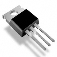
IRF830
Features
■ ■
Extremely high dv/dt capability Low Gate Charge Qg results in Simple Drive Requirement 100% avalanche tested Gate charge minimized Very low intrinsic capacitances Very good manufacturing repeatability
VDSS = 500V ID = 5A RDS(ON) = 1.2Ω
■ ■ ■ ■
Description
The IRF830 is a new generation of high voltage N–Channel enhancement mode power MOSFETs and is obtained through an extreme optimization layout design, in additional to pushing on-resistance significantly down, special care is taken to ensure a very good dv/dt capability, provide superior switching performance, withstand high energy pulse in the avalanche, and increases packing density. IRF830 TOP View (TO220)
Application
■ ■ ■
High current, high speed switching Lighting Ideal for off-line power supply, adaptor, PFC
Absolute Maximum Ratings
Parameter ID@Tc=25 ْC ID@Tc=100ْC IDM PD@TC=25ْC VGS EAS IAR EAR dv/dt TJ TSTG Continuous Drain Current,VGS@10V Continuous Drain Current,VGS@10V Pulsed Drain Current Power Dissipation Linear Derating Factor Gate-to-Source Voltage Single Pulse Avalanche Energy Avalanche Current
① ① ③ ② ①
Max. 5 3 20 80 0.67 ±30 120 5 8.5 4.5 –55 to +150
Units A W W/ ْC V mJ A mJ V/ns ْC
Repetitive Avalanche Energy Peak Diode Recovery dv/dt Operating Junction and Storage Temperature Range
Thermal Resistance
Parameter RθJC RθCS RθJA Junction-to-case Case-to-Sink,Flat,Greased Surface Junction-to-Ambient Min. — — — Typ. — 0.50 — Max. 1.56 — 62.5 ْC/W Units
1
�IRF830
Electrical Characteristics @TJ=25 ْC(unless otherwise specified)
Parameter V(BR)DSS RDS(on) VGS(th) gfs IDSS IGSS Qg Qgs Qgd td(on) tr td(off) tf Ciss Coss Crss Drain-to-Source Breakdown Voltage Static Drain-to-Source On-resistance Gate Threshold Voltage Forward Transconductance Drain-to-Source Leakage current Gate-to-Source Forward leakage Gate-to-Source Reverse leakage Total Gate Charge Gate-to-Source charge Gate-to-Drain("Miller") charge Turn-on Delay Time Rise Time Turn-Off Delay Time Fall Time Input Capacitance Output Capacitance Reverse Transfer Capacitance
△V(BR)DSS/△TJ Breakdown Voltage Temp.Coefficient
Min. 500 — — 2.0 — — — — — — — — — — — — — — —
Typ. — 0.6 1.15 — 4.3 — — — — 11 3 5 13 22 28 20 515 55 6.5
Max. Units — — 1.2 4.0 — 1 10 100 -100 15 — — 36 54 66 50 670 72 8.5 V
Test Conditions VGS=0V,ID=250μA
④
V/ْC Reference to 25ْC,ID=250μA Ω VGS=10V,ID=2.5A V S μA nA VDS=VGS,ID=250μA VDS=40V,ID=2.25A VDS=500V,VGS=0V VDS=400V,VGS=0V,TJ=150ْC VGS=30V VGS=-30V
ID=5A nC VDS=400V VGS=10V VDD=250V ID=5A nS RG=25Ω VGS=0V pF VDS=25V f=1.0MHZ
Source-Drain Ratings and Characteristics
Parameter IS ISM VSD Trr Qrr Continuous Source Current (Body Diode) Pulsed Source Current (Body Diode) ① Diode Forward Voltage Reverse Recovery Time Reverse Recovery Charge . . Min. — — — — — Typ. — — — 300 1.8 Max. 5 A 20 1.4 — V nS uC Units Test Conditions MOSFET symbol showing the integral reverse p-n junction diode. TJ=25ْC,IS=5A,VGS=0V ④ TJ=25ْC,IF=5A di/dt=100A/μs ④
Notes: ① Repetitive rating; pulse width limited by maxIimum. junction temperature ② L = 15mH, IAS =4 A, VDD = 50V, RG = 25Ω, Starting TJ = 25°C
③ ISD≤5A,di/dt≤200A/μs, VDD≤V(BR)DSS, TJ≤25 ْC ④ Pulse width≤300μS; duty cycle≤2%
2
�IRF830
Typical Performance Characteristics
Figure 1 On-Region Characteristics
Figure 2 Transfer Characteristics
Figure 3 On-Resistance Variation vs. Drain Current and Gate Voltage
Figure 4 Body diode forward Voltage Variation vs. Source Current and temperature
Figure 5 Capacitance Characteristics
Figure 6 Gate Charge Characteristics 3
�IRF830
Typical Performance Characteristics
Figure 7 Breakdown Voltage Variation vs. Temperature
Figure 8 On-Resistance Variation vs. Temperature
Figure 9 Maximum Safe Operation Area
Figure 10 Maximum Drain Current vs. Case Temperature
Figure 12 Transient Thermal Response Curve 4
�IRF830
Test Circuit and Waveform
Gate Charge Test Circuit & Waveform
Resistive Switching Test Circuit & Waveform
Unclamped Inductive Switching Test Circuit & Waveform
5
�IRF830
Mechanical Dimensions
TO-220
6
�
很抱歉,暂时无法提供与“IRF830”相匹配的价格&库存,您可以联系我们找货
免费人工找货