Data Sheet
Comlinear CLC1606
®
1.3GHz Current Feedback Amplifier
The COMLINEAR CLC1606 is a high-performance, current feedback amplifier
with superior bandwith and video specifications. The CLC1606 provides
1.3GHz unity gain bandwidth, ±0.1dB gain flatness to 150MHz, and provides
3,300V/μs slew rate exceeding the requirements of high-definition television
(HDTV) and other multimedia applications. The COMLINEAR CLC1606 highperformance amplifier also provide ample output current to drive multiple
video loads.
The COMLINEAR CLC1606 is designed to operate from ±5V or +5V supplies.
It consumes only 7.5mA of supply current. The combination of high-speed
and excellent video performance make the CLC1606 well suited for use in
many general purpose, high-speed applications including standard definition
and high definition video. Data communications applications benefit from
the CLC1606’s total harmonic distortion of -68dBc at 10MHz and fast settling
time to 0.1%.
APPLICATIONS
n RGB video line drivers
n High definition video driver
n Video switchers and routers
n ADC buffer
n Active filters
n High-speed instrumentation
n Wide dynamic range IF amp
Typical Application - Driving Dual Video Loads
Comlinear CLC1606 1.3GHz Current Feedback Amplifier
General Description
FEATURES
n 1.2GHz -3dB bandwidth at G=2
n 3,300V/μs slew rate
n 0.01%/0.01˚ differential gain/
phase error
n 7.5mA supply current
n 875MHz large signal bandwidth
n 120mA output current (easily drives
three video loads)
n Fully specified at 5V and ±5V supplies
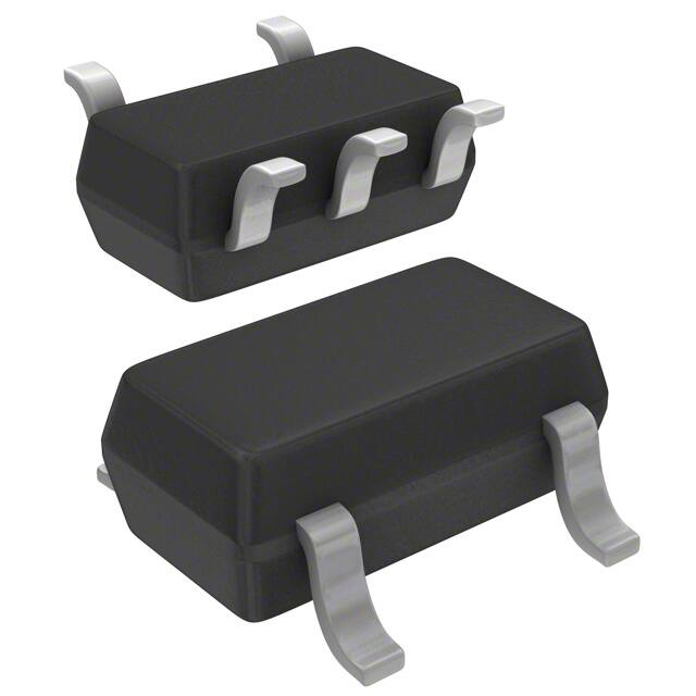
n CLC1606: Pb-free SOT23-5
n CLC1606: Pb-free SOIC-8
Rev 1D
Ordering Information
Part Number
Package
Pb-Free
RoHS Compliant
Operating Temperature Range
Packaging Method
CLC1606IST5X
SOT23-5
Yes
Yes
-40°C to +85°C
Reel
CLC1606ISO8
SOIC-8
Yes
Yes
-40°C to +85°C
Rail
CLC1606ISO8X
SOIC-8
Yes
Yes
-40°C to +85°C
Reel
Moisture sensitivity level for all parts is MSL-1.
Exar Corporation
48720 Kato Road, Fremont CA 94538, USA
www.exar.com
Tel. +1 510 668-7000 - Fax. +1 510 668-7001
�Data Sheet
SOT23-5 Pin Assignments
SOT23-5 Pin Configuration
1
-V S
2
+IN
3
+
5
+VS
4
-IN
-
SOIC Pin Configuration
Pin Name
1
OUT
Output
2
-VS
Negative supply
3
+IN
Positive input
4
-IN
Negative input
5
+VS
Positive supply
SOIC Pin Assignments
Pin No.
NC
1
8
NC
-IN1
2
7
+VS
+IN1
3
6
OUT
-V S
4
Description
Comlinear CLC1606 1.3GHz Current Feedback Amplifier
OUT
Pin No.
5
NC
Pin Name
Description
1
NC
No connect
2
-IN1
Negative input, channel 1
3
+IN1
Positive input, channel 1
4
-VS
Negative supply
5
NC
No connect
6
OUT
Output
7
+VS
Positive supply
8
NC
No connect
Rev 1D
©2007-2013 Exar Corporation
2/18
Rev 1D
�Data Sheet
Absolute Maximum Ratings
The safety of the device is not guaranteed when it is operated above the “Absolute Maximum Ratings”. The device
should not be operated at these “absolute” limits. Adhere to the “Recommended Operating Conditions” for proper device function. The information contained in the Electrical Characteristics tables and Typical Performance plots reflect the
operating conditions noted on the tables and plots.
Supply Voltage
Input Voltage Range
Continuous Output Current
Min
Max
Unit
0
-Vs -0.5V
14
+Vs +0.5V
120
V
V
mA
Comlinear CLC1606 1.3GHz Current Feedback Amplifier
Parameter
Reliability Information
Parameter
Min
Junction Temperature
Storage Temperature Range
Lead Temperature (Soldering, 10s)
Package Thermal Resistance
5-Lead SOT23
8-Lead SOIC
Typ
-65
Max
Unit
150
150
260
°C
°C
°C
221
100
°C/W
°C/W
Notes:
Package thermal resistance (qJA), JDEC standard, multi-layer test boards, still air.
ESD Protection
Product
SOT23-5
Human Body Model (HBM)
Charged Device Model (CDM)
2kV
1kV
(1)
Notes:
1. 0.8kV between the input pairs +IN and -IN pins only. All other pins are 2kV.
Recommended Operating Conditions
Min
Operating Temperature Range
Supply Voltage Range
-40
4.5
©2007-2013 Exar Corporation
3/18
Typ
Max
Unit
+85
12
°C
V
Rev 1D
Parameter
Rev 1D
�Data Sheet
Electrical Characteristics at +5V
TA = 25°C, Vs = +5V, Rf = 270Ω, RL = 150Ω to VS/2, G = 2; unless otherwise noted.
Symbol
Parameter
Conditions
Min
Typ
Max
Units
Frequency Domain Response
UGBW
-3dB Bandwidth
1000
MHz
BWSS
-3dB Bandwidth
G = +2, VOUT = 0.5Vpp
900
MHz
BWLS
Large Signal Bandwidth
G = +2, VOUT = 1Vpp
800
MHz
BW0.1dBSS
0.1dB Gain Flatness
G = +2, VOUT = 0.5Vpp
132
MHz
BW0.1dBLS
0.1dB Gain Flatness
G = +2, VOUT = 1Vpp
140
MHz
Time Domain Response
tR, tF
Rise and Fall Time
VOUT = 1V step; (10% to 90%)
0.6
ns
tS
Settling Time to 0.1%
VOUT = 1V step
10
ns
OS
Overshoot
VOUT = 0.2V step
1
%
SR
Slew Rate
1V step
1500
V/µs
Distortion/Noise Response
HD2
2nd Harmonic Distortion
1Vpp, 5MHz
-74
dBc
HD3
3rd Harmonic Distortion
1Vpp, 5MHz
-70
dBc
THD
Total Harmonic Distortion
1Vpp, 5MHz
68
dB
IP3
Third-Order Intercept
1Vpp, 10MHz
36
dBm
DG
Differential Gain
NTSC (3.58MHz), AC-coupled, RL = 150Ω
0.01
%
DP
Differential Phase
NTSC (3.58MHz), AC-coupled, RL = 150Ω
0.01
°
en
Input Voltage Noise
> 1MHz
3
nV/√Hz
ini
Input Current Noise
> 1MHz, Inverting
20
pA/√Hz
> 1MHz, Non-inverting
30
pA/√Hz
0
mV
3.7
µV/°C
DC Performance
VIO
dVIO
Ibn
dIbn
Ibi
dIbi
Input Offset Voltage
Average Drift
Input Bias Current - Non-Inverting
Average Drift
Input Bias Current - Inverting
Average Drift
Power Supply Rejection Ratio
IS
Supply Current
DC
µA
100
nA/°C
±6.0
µA
56
nA/°C
55
dB
6.5
mA
150
kΩ
Input Characteristics
RIN
Input Resistance
CIN
Input Capacitance
CMIR
Common Mode Input Range
CMRR
Common Mode Rejection Ratio
Non-inverting
Inverting
70
Ω
1.0
pF
±1.5
V
DC
50
dB
0.1
Ω
Output Characteristics
RO
Output Resistance
Closed Loop, DC
VOUT
Output Voltage Swing
RL = 150Ω
IOUT
Output Current
©2007-2013 Exar Corporation
4/18
±1.5
V
±120
mA
Rev 1D
Rev 1D
PSRR
±3.0
Comlinear CLC1606 1.3GHz Current Feedback Amplifier
G = +1, Rf = 390Ω, VOUT = 0.5Vpp
�Data Sheet
Electrical Characteristics at ±5V
TA = 25°C, Vs = ±5V, Rf = 270Ω, RL = 150Ω, G = 2; unless otherwise noted.
Symbol
Parameter
Conditions
Min
Typ
Max
Units
Frequency Domain Response
-3dB Bandwidth
G = +1, Rf = 390Ω, VOUT = 0.5Vpp
1300
MHz
BWSS
-3dB Bandwidth
G = +2, VOUT = 0.5Vpp
1200
MHz
BWLS
Large Signal Bandwidth
G = +2, VOUT = 2Vpp
875
MHz
BW0.1dBSS
0.1dB Gain Flatness
G = +2, VOUT = 0.5Vpp
150
MHz
BW0.1dBLS
0.1dB Gain Flatness
G = +2, VOUT = 2Vpp
150
MHz
Time Domain Response
tR, tF
Rise and Fall Time
VOUT = 2V step; (10% to 90%)
0.5
ns
tS
Settling Time to 0.1%
VOUT = 2V step
13
ns
OS
Overshoot
VOUT = 0.2V step
1
%
SR
Slew Rate
2V step
3300
V/µs
Distortion/Noise Response
HD2
2nd Harmonic Distortion
2Vpp, 5MHz
-71
dBc
HD3
3rd Harmonic Distortion
2Vpp, 5MHz
-71
dBc
THD
Total Harmonic Distortion
2Vpp, 5MHz
-68
dB
IP3
Third-Order Intercept
2Vpp, 10MHz
39
dBm
DG
Differential Gain
NTSC (3.58MHz), AC-coupled, RL = 150Ω
0.01
%
DP
Differential Phase
NTSC (3.58MHz), AC-coupled, RL = 150Ω
0.01
°
en
Input Voltage Noise
> 1MHz
3
nV/√Hz
ini
Input Current Noise - Inverting
> 1MHz, Inverting
20
pA/√Hz
> 1MHz, Non-inverting
30
pA/√Hz
DC Performance
VIO
dVIO
Ibn
dIbn
Ibi
dIbi
Input Offset Voltage(1)
-10
0.5
-45
±3.0
Average Drift
3.7
Input Bias Current - Non-Inverting (1)
Average Drift
-50
Average Drift
IS
Supply Current
DC
40
50
µA
56
nA/°C
50
dB
7.5
(1)
µA
nA/°C
9.5
mA
Input Characteristics
RIN
Input Resistance
CIN
Input Capacitance
CMIR
Common Mode Input Range
CMRR
Common Mode Rejection Ratio (1)
Non-inverting
150
Inverting
170
k
1.0
pF
DC
40
kΩ
±4.0
V
50
dB
0.1
Ω
Output Characteristics
RO
Output Resistance
Closed Loop, DC
VOUT
Output Voltage Swing
RL = 150Ω
IOUT
Output Current
±3.0
(1)
±3.7
V
±280
mA
Notes:
1. 100% tested at 25°C
©2007-2013 Exar Corporation
5/18
Rev 1D
Rev 1D
Power Supply Rejection Ratio (1)
±7.0
mV
µV/°C
45
100
Input Bias Current - Inverting (1)
PSRR
10
Comlinear CLC1606 1.3GHz Current Feedback Amplifier
UGBW
�Data Sheet
Typical Performance Characteristics
TA = 25°C, Vs = ±5V, Rf = 270Ω, RL = 150Ω, G = 2; unless otherwise noted.
Non-Inverting Frequency Response
Inverting Frequency Response
0
0
Normalized Gain (dB)
Normalized Gain (dB)
G = -1
G=1
Rf = 499Ω
G=2
-3
G=5
G = 10
-6
G = -2
G = -5
-3
G = -10
-6
VOUT = 0.5Vpp
VOUT = 0.5Vpp
-9
-9
0.1
1
10
100
1000
0.1
1
Frequency (MHz)
100
1000
Frequency Response vs. RL
1
6
5
0
4
Normalized Gain (dB)
CL = 1000pF
Rs = 3.3Ω
-1
Normalized Gain (dB)
10
Frequency (MHz)
Frequency Response vs. CL
CL = 500pF
Rs = 5Ω
-2
-3
CL = 100pF
Rs = 10Ω
-4
CL = 50pF
Rs = 15Ω
-5
-6
3
2
1
0
-1
RL = 100Ω
-2
RL = 50Ω
-3
-4
CL = 20pF
Rs = 20Ω
VOUT = 0.5Vpp
VOUT = 0.5Vpp
-5
-7
RL = 25Ω
-6
0.1
1
10
100
1000
0.1
1
10
100
1000
Rev 1D
Frequency (MHz)
Frequency (MHz)
Frequency Response vs. VOUT
Frequency Response vs. Temperature
3
2
2
1
1
0
Normalized Gain (dB)
Normalized Gain (dB)
Comlinear CLC1606 1.3GHz Current Feedback Amplifier
3
G=1
Rf = 390Ω
3
0
-1
VOUT = 1Vpp
-2
VOUT = 2Vpp
-3
-4
VOUT = 4Vpp
-5
-1
+ 25degC
-2
- 40degC
-3
+ 85degC
-4
-5
VOUT = 0.2Vpp
-6
-6
-7
-7
0.1
1
10
100
1000
0.1
Frequency (MHz)
©2007-2013 Exar Corporation
1
10
100
1000
10000
Frequency (MHz)
6/18
Rev 1D
�Data Sheet
Typical Performance Characteristics
TA = 25°C, Vs = ±5V, Rf = 270Ω, RL = 150Ω, G = 2; unless otherwise noted.
Non-Inverting Frequency Response at VS = 5V
2
Inverting Frequency Response at VS = 5V
G = -1
0
G=2
Normalized Gain (dB)
Normalized Gain (dB)
0
-1
-2
-3
G=5
-4
-5
G = 10
-6
G = -2
G = -5
-3
G = -10
-6
-7
VOUT = 0.5Vpp
-8
VOUT = 0.5Vpp
-9
-9
0.1
1
10
100
1000
0.1
1
Frequency (MHz)
100
1000
Frequency Response vs. RL at VS = 5V
1
4
3
0
2
Normalized Gain (dB)
CL = 1000pF
Rs = 3.3Ω
-1
Normalized Gain (dB)
10
Frequency (MHz)
Frequency Response vs. CL at VS = 5V
CL = 500pF
Rs = 5Ω
-2
-3
CL = 100pF
Rs = 10Ω
-4
CL = 50pF
Rs = 15Ω
-5
-6
VOUT = 0.5Vpp
1
0
-1
RL = 100Ω
-2
RL = 50Ω
-3
-4
CL = 20pF
Rs = 20Ω
RL = 25Ω
VOUT = 0.5Vpp
-5
-7
-6
0.1
1
10
100
1000
0.1
1
1
0
0
Normalized Gain (dB)
2
1
-1
VOUT = 1Vpp
VOUT = 2Vpp
-4
VOUT = 3Vpp
-5
1000
Frequency Response vs. Temperature at VS = 5V
2
-3
100
Frequency (MHz)
Frequency Response vs. VOUT at VS = 5V
-2
10
Rev 1D
Frequency (MHz)
Normalized Gain (dB)
Comlinear CLC1606 1.3GHz Current Feedback Amplifier
3
G=1
Rf = 390Ω
1
-1
-2
+ 25degC
-3
- 40degC
-4
-5
-6
+ 85degC
VOUT = 0.2Vpp
-6
-7
-7
0.1
1
10
100
1000
0.1
Frequency (MHz)
©2007-2013 Exar Corporation
1
10
100
1000
10000
Frequency (MHz)
7/18
Rev 1D
�Data Sheet
Typical Performance Characteristics - Continued
TA = 25°C, Vs = ±5V, Rf = 270Ω, RL = 150Ω, G = 2; unless otherwise noted.
Gain Flatness
Gain Flatness at VS = 5V
0.8
0.7
0.6
0.5
1.1
Normalized Gain (dB)
Normalized Gain (dB)
1.3
0.9
0.7
0.5
0.3
0.1
0.4
0.3
0.2
0.1
0
-0.1
-0.2
-0.1
VOUT = 2Vpp
RL = 150Ω
Rf = 270Ω
-0.3
VOUT = 2Vpp
RL = 150Ω
Rf = 270Ω
-0.3
-0.4
-0.5
-0.5
0.1
1
10
100
1000
0.1
1
10
Frequency (MHz)
100
1000
Frequency (MHz)
-3dB Bandwidth vs. VOUT at G=10
-3dB Bandwidth vs. VOUT at G=10, VS = 5V
600
450
-3dB Bandwidth (MHz)
-3dB Bandwidth (MHz)
550
500
450
400
400
350
300
350
G = 10
300
250
0.0
0.5
1.0
1.5
2.0
2.5
3.0
3.5
4.0
0.0
0.5
2.0
2.5
3.0
Input Voltage Noise
2.0
20
VS = ±5.0V
Input Voltage Noise (nV/√Hz)
Output Resistance (Ω)
1.5
VOUT (VPP)
Closed Loop Output Impedance vs. Frequency
1.8
1.0
Rev 1D
VOUT (VPP)
1.6
1.4
1.2
1.0
0.8
0.6
0.4
0.2
0
10K
100K
1M
10M
10
5
0.001
0.01
0.1
1
10
Frequency (MHz)
Frequency (Hz)
©2007-2013 Exar Corporation
15
0
0.0001
100M
8/18
Comlinear CLC1606 1.3GHz Current Feedback Amplifier
1.7
1.5
Rev 1D
�Data Sheet
Typical Performance Characteristics - Continued
TA = 25°C, Vs = ±5V, Rf = 270Ω, RL = 150Ω, G = 2; unless otherwise noted.
2nd Harmonic Distortion vs. RL
3rd Harmonic Distortion vs. RL
-55
-60
-60
RL = 150Ω
-65
RL = 150Ω
-70
Distortion (dBc)
Distortion (dBc)
-65
-75
-80
-85
RL = 499Ω
-90
-70
-75
-80
RL = 499Ω
-85
-90
-95
-95
VOUT = 2Vpp
-100
VOUT = 2Vpp
-100
0
5
10
15
20
0
5
Frequency (MHz)
2nd Harmonic Distortion vs. VOUT
15
20
3rd Harmonic Distortion vs. VOUT
-60
-60
-65
-65
-75
10MHz
-70
10MHz
-70
Distortion (dBc)
Distortion (dBc)
10
Frequency (MHz)
5MHz
-80
-75
5MHz
-80
-85
1MHz
-85
-90
RL = 150Ω
-90
0.5
0.75
1MHz
RL = 150Ω
-95
1
1.25
1.5
1.75
2
2.25
2.5
0.5
0.75
1
1.25
1.5
1.75
2
2.25
2.5
Rev 1D
Output Amplitude (Vpp)
Output Amplitude (Vpp)
CMRR vs. Frequency
PSRR vs. Frequency
0
0
-10
-10
-20
-20
PSRR (dB)
CMRR (dB)
VS = ±5.0V
-30
-40
-50
-30
-40
-50
-60
-60
10k
100k
Comlinear CLC1606 1.3GHz Current Feedback Amplifier
-55
1M
10M
10K
100M
©2007-2013 Exar Corporation
100K
1M
10M
100M
Frequency (Hz)
Frequency (Hz)
9/18
Rev 1D
�Data Sheet
Typical Performance Characteristics - Continued
TA = 25°C, Vs = ±5V, Rf = 270Ω, RL = 150Ω, G = 2; unless otherwise noted.
Small Signal Pulse Response at VS = 5V
0.125
2.625
0.1
2.6
0.075
2.575
2.55
0.025
2.525
Voltage (V)
0.05
0
-0.025
2.5
2.475
-0.05
2.45
-0.075
2.425
-0.1
2.4
-0.125
2.375
0
20
40
60
80
100
120
140
160
180
200
0
20
40
60
80
Time (ns)
120
140
160
180
200
Large Signal Pulse Response at VS = 5V
3
4
2
3.5
1
3
Voltage (V)
Voltage (V)
Large Signal Pulse Response
0
2.5
-1
2
-2
1.5
-3
1
0
20
40
60
80
100
120
140
160
180
200
0
20
40
60
120
140
160
180
200
Differential Gain & Phase DC Coupled Output
0.06
0.015
0.05
Diff Gain (%) / Diff Phase (°)
0.02
0.01
DG
0
DP
-0.005
-0.01
100
Time (ns)
Differential Gain & Phase AC Coupled Output
0.005
80
DP
0.04
0.03
0.02
0.01
DG
0
-0.01
RL = 150Ω
AC coupled
-0.015
RL = 150Ω
DC coupled
-0.02
-0.7
-0.5
-0.3
-0.1
0.1
0.3
0.5
0.7
-0.7
Input Voltage (V)
©2007-2013 Exar Corporation
-0.5
-0.3
-0.1
0.1
0.3
0.5
0.7
Input Voltage (V)
10/18
Rev 1D
Rev 1D
Time (ns)
Diff Gain (%) / Diff Phase (°)
100
Time (ns)
Comlinear CLC1606 1.3GHz Current Feedback Amplifier
Voltage (V)
Small Signal Pulse Response
�Data Sheet
Typical Performance Characteristics - Continued
TA = 25°C, Vs = ±5V, Rf = 270Ω, RL = 150Ω, G = 2; unless otherwise noted.
Differential Gain & Phase DC Coupled at VS = ±2.5V
0.05
0.005
0.04
0
Diff Gain (%) / Diff Phase (°)
0.01
DP
-0.005
-0.01
-0.015
DG
-0.02
-0.025
RL = 150Ω
DC coupled
AC
-0.35
0.02
0.01
0
-0.01
DG
-0.02
-0.03
-0.03
DP
0.03
RL = 150Ω
DC coupled
-0.04
-0.25
-0.15
-0.05
0.05
0.15
0.25
0.35
-0.35
Input Voltage (V)
-0.25
-0.15
-0.05
0.05
0.15
0.25
0.35
Input Voltage (V)
Comlinear CLC1606 1.3GHz Current Feedback Amplifier
Diff Gain (%) / Diff Phase (°)
Differential Gain & Phase AC Coupled Output at VS = ±2.5V
Rev 1D
©2007-2013 Exar Corporation
11/18
Rev 1D
�Data Sheet
General Information - Current Feedback
Technology
Advantages of CFB Technology
CFB also alleviates the traditional trade-off between
closed loop gain and usable bandwidth that is seen with
a VFB amplifier. With CFB, the bandwidth is primarily
determined by the value of the feedback resistor, Rf. By
using optimum feedback resistor values, the bandwidth
of a CFB amplifier remains nearly constant with different
gain configurations.
When designing with CFB amplifiers always abide by these
basic rules:
• Use the recommended feedback resistor value
• Do not use reactive (capacitors, diodes, inductors, etc.)
elements in the direct feedback path
• Avoid stray or parasitic capacitance across feedback
resistors
• Follow general high-speed amplifier layout guidelines
VIN
Ierr
x1
Zo*Ierr
VOUT
Rf
RL
Rg
VOUT
VIN
= 1+
Rf
Rg
+
1+
1
Rf
Eq. 1
Zo(jω)
Figure 1. Non-Inverting Gain Configuration with First
Order Transfer Function
©2007-2013 Exar Corporation
VIN
Rg
VOUT
VIN
VOUT
Rf
= −
Rf
Rg
+
1+
1
Rf
RL
Eq. 2
Zo(jω)
Figure 2. Inverting Gain Configuration with First Order
Transfer Function
CFB Technology - Theory of Operation
Figure 1 shows a simple representation of a current
feedback amplifier that is configured in the traditional
non-inverting gain configuration.
Instead of having two high-impedance inputs similar to a
VFB amplifier, the inputs of a CFB amplifier are connected
across a unity gain buffer. This buffer has a high impedance
input and a low impedance output. It can source or sink
current (Ierr) as needed to force the non-inverting input
to track the value of Vin. The CFB architecture employs
a high gain trans-impedance stage that senses Ierr and
drives the output to a value of (Zo(jω) * Ierr) volts. With
the application of negative feedback, the amplifier will
drive the output to a voltage in a manner which tries to
drive Ierr to zero. In practice, primarily due to limitations
on the value of Zo(jω), Ierr remains a small but finite
value.
A closer look at the closed loop transfer function (Eq.1)
shows the effect of the trans-impedance, Zo(jω) on the
gain of the circuit. At low frequencies where Zo(jω) is very
large with respect to Rf, the second term of the equation
approaches unity, allowing Rf and Rg to set the gain. At
higher frequencies, the value of Zo(jω) will roll off, and
the effect of the secondary term will begin to dominate.
The -3dB small signal parameter specifies the frequency
where the value Zo(jω) equals the value of Rf causing the
gain to drop by 0.707 of the value at DC.
For more information regarding current feedback
amplifiers, visit www.cadeka.com for detailed application
notes, such as AN-3: The Ins and Outs of Current Feedback
Amplifiers.
12/18
Rev 1D
Rev 1D
• Ensure proper precautions have been made for driving
capacitive loads
Ierr
Zo*Ierr
Comlinear CLC1606 1.3GHz Current Feedback Amplifier
The CLC1606 Family of amplifiers utilize current feedback
(CFB) technology to achieve superior performance. The
primary advantage of CFB technology is higher slew rate
performance when compared to voltage feedback (VFB)
architecture. High slew rate contributes directly to better
large signal pulse response, full power bandwidth, and
distortion.
x1
�Data Sheet
Application Information
Basic Operation
+Vs
Input
Feedback Resistor Selection
6.8μF
0.1μF
+
Output
-
RL
0.1μF
Rg
Rf
6.8μF
G = 1 + (Rf/Rg)
-Vs
Figure 3. Typical Non-Inverting Gain Circuit
+Vs
R1
Input
0.1μF
+
Rg
6.8μF
One of the key design considerations when using a CFB
amplifier is the selection of the feedback resistor, Rf. Rf is
used in conjunction with Rg to set the gain in the traditional
non-inverting and inverting circuit configurations. Refer to
figures 3 and 4. As discussed in the Current Feedback
Technology section, the value of the feedback resistor has
a pronounced effect on the frequency response of the
circuit.
Table 1, provides recommended Rf and associated Rg
values for various gain settings. These values produce
the optimum frequency response, maximum bandwidth
with minimum peaking. Adjust these values to optimize
performance for a specific application. The typical
performance characteristics section includes plots that
illustrate how the bandwidth is directly affected by the
value of Rf at various gain settings.
Output
-
RL
0.1μF
Rf
G = - (Rf/Rg)
-Vs
For optimum input offset
voltage set R1 = Rf || Rg
Figure 4. Typical Inverting Gain Circuit
+Vs
Input
6.8μF
0.1μF
+
Output
0.1μF
6.8μF
-Vs
RL
Rf
G=1
Rf is required for CFB amplifiers
Figure 5. Typical Unity Gain (G=1) Circuit
©2007-2013 Exar Corporation
Rf (Ω)
Rg (Ω)
±0.1dB BW
(MHz)
-3dB BW
(MHz)
1
390
-
136
1300
2
270
270
150
1200
5
270
67.5
115
750
Rev 1D
6.8μF
Gain
(V/V
Table 1: Recommended Rf vs. Gain
In general, lowering the value of Rf from the recommended
value will extend the bandwidth at the expense of
additional high frequency gain peaking. This will cause
increased overshoot and ringing in the pulse response
characteristics. Reducing Rf too much will eventually
cause oscillatory behavior.
Increasing the value of Rf will lower the bandwidth.
Lowering the bandwidth creates a flatter frequency
response and improves 0.1dB bandwidth performance.
This is important in applications such as video. Further
increase in Rf will cause premature gain rolloff and
adversely affect gain flatness.
13/18
Comlinear CLC1606 1.3GHz Current Feedback Amplifier
Figures 3, 4, and 5 illustrate typical circuit configurations for
non-inverting, inverting, and unity gain topologies for dual
supply applications. They show the recommended bypass
capacitor values and overall closed loop gain equations.
CFB amplifiers can be used in unity gain configurations.
Do not use the traditional voltage follower circuit, where
the output is tied directly to the inverting input. With a CFB
amplifier, a feedback resistor of appropriate value must be
used to prevent unstable behavior. Refer to figure 5 and
Table 1. Although this seems cumbersome, it does allow a
degree of freedom to adjust the passband characteristics.
Rev 1D
�Data Sheet
Driving Capacitive Loads
Input
+
Rs
-
Output
CL
Rf
RL
Rg
Overdrive Recovery
An overdrive condition is defined as the point when either
one of the inputs or the output exceed their specified
voltage range. Overdrive recovery is the time needed for
the amplifier to return to its normal or linear operating
point. The recovery time varies, based on whether the
input or output is overdriven and by how much the range
is exceeded. The CLC1606 Family will typically recover
in less than 10ns from an overdrive condition. Figure 7
shows the CLC1606 in an overdriven condition.
Figure 6. Addition of RS for Driving
Capacitive Loads
CL (pF)
RS (Ω)
-3dB BW (MHz)
20
20
375
100
10
180
1000
3.3
58
6
VIN = 2Vpp
G=5
1
4
Input Voltage (V)
Input
Output
0.5
2
0
0
-0.5
-2
-1
-4
-1.5
Output Voltage (V)
Table 2 provides the recommended RS for various
capacitive loads. The recommended RS values result
in


 工商网监
湘ICP备2023018690号
工商网监
湘ICP备2023018690号

