S P6 2 6 0
200mA RF Low Noise LDO Regulator
January 2011
Rev. 2.1.0
GENERAL DESCRIPTION
APPLICATIONS
The SP6260 family is a series of CMOS positive
low noise voltage regulators capable of
delivering up to 200mA of continuous current.
Each of these devices consists of a voltage
reference, an error amplifier, a resistor
network for setting the output voltage, a
current limit circuit for current protection and
a chip enable circuit.
The SP6260 series feature high ripple
rejection, low dropout voltage, low noise, high
output voltage accuracy and low current
consumption which make them ideal for use in
various
battery-powered
and
hand-held
devices.
The SP6260 series is offered in the following
fixed output voltage options: 1.2V, 1.5V, 1.8V,
2.5V, 2.8V, 3.0V, 3.2V and 3.3V.
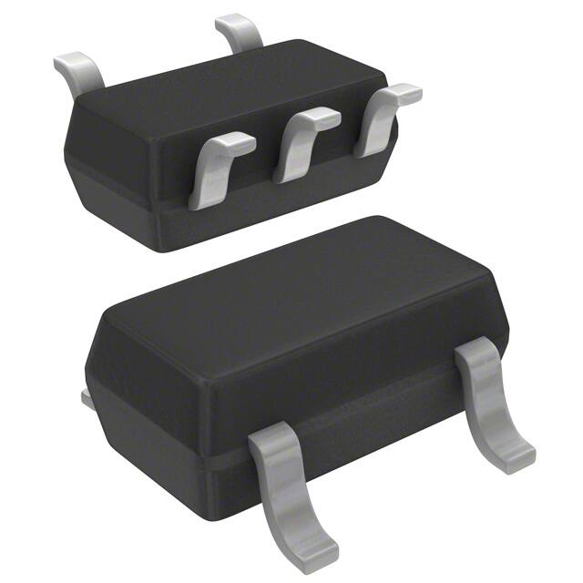
The SP6260 family is available in standard
lead free, RoHS compliant 5-pin SOT-23
package.
• Hand Held Equipments
• Wireless Communication Devices
• Battery Powered Equipments
• Industrial and Medical Equipments
FEATURES
• 200mA Continuous Output Current
− 150mV Dropout Voltage @ IOUT=100mA
(Except 1.2V and 1.5V Version)
− 1.2V to 3.3V Fixed Output Voltages
− ±2% Output Voltage Accuracy
• 2V Minimum Input Voltage
• 30µVrms Output Noise (10Hz-100KHz)
• 70dB Power Supply Rejection Ratio
• 4mV Line Regulation (typ)
• 12mV Load Regulation (typ)
• Low Standby Current: 0.1µA Typical
• Low Quiescent Current: 25µA Typical
• Lead Free, RoHS Compliant
5-pin SOT-23 Package
TYPICAL APPLICATION DIAGRAM
Fig. 1: SP6260 Application Diagram
Exar Corporation
48720 Kato Road, Fremont CA 94538, USA
www.exar.com
Tel. +1 510 668-7000 – Fax. +1 510 668-7001
�S P6 2 6 0
200mA RF Low Noise LDO Regulator
ABSOLUTE MAXIMUM RATINGS
OPERATING RATINGS
These are stress ratings only and functional operation of
the device at these ratings or any other above those
indicated in the operation sections of the specifications
below is not implied. Exposure to absolute maximum
rating conditions for extended periods of time may affect
reliability.
Input Voltage Range VIN .................................2.0 to 6.0V
Junction Temperature Range TJ.................. -40°C to 85°C
Thermal Resistance θJA .....................................250°C/W
Thermal Resistance θJC ...................................... 74°C/W
Input Voltage VIN ................................................... 6.5V
Enable Pin Input Voltage ........................-0.3 to VIN+0.3V
Output Current................................................... 300mA
Junction Temperature .......................................... 150°C
Storage Temperature Range .................... -65°C to 150°C
Lead Soldering (Sold. 10sec) ................................ 260°C
ESD Rating (HBM - Human Body Model) .................... 2kV
ESD Rating (MM - Machine Model) ...........................200V
ELECTRICAL SPECIFICATIONS
Specifications with standard type are for an Operating Junction Temperature of TJ = 25°C only; limits applying over the full
Operating Junction Temperature range of -40°C to 85°C are denoted by a “•”. Minimum and Maximum limits are guaranteed
through test, design, or statistical correlation. Typical values represent the most likely parametric norm at TJ = 25°C, and
are provided for reference purposes only.
SP6260HEK (1.2V)
Unless otherwise indicated, VIN = 2.2V, CIN = 1µF, COUT = 1µF.
Parameter
Output Voltage VOUT
Min.
Typ.
Max.
Units
1.176
1.2
1.224
V
Input Voltage VIN
Output Current IOUT
6
200
Conditions
VIN=2.2V
1mA≤IOUT≤30mA
V
mA
VIN—VOUT=1V
Load Regulation VRLOAD
12
40
mV
VIN=2.2V
1mA≤IOUT≤80mA
Line Regulation VRLINE
4
16
mV
2.2V≤VIN=≤6V
IOUT=30mA
Dropout Voltage VDROP
Quiescent Current IQ
700
900
700
900
700
900
700
900
25
50
Standby Current ISTD
0.1
Power Supply Rejection Ratio
PSRR
70
1
IOUT=10mA
IOUT=100mA
mV
IOUT=150mA
IOUT=200mA
µA
VIN=2.2V,IOUT=0mA
µA
VIN=2.2V
VCE in OFF mode
dB
Ripple 0.5Vp-p, f=10kHz
VIN=2.5V
Output Voltage
Temperature Coefficient
±120
µV/°C
•
ΔVOUT/ΔT
±100
ppm/°C
•
(ΔVOUT/VOUT)/ΔT
Short Current Limit ILIMIT
50
mA
RMS Output Noise VNOISE
CE “High” Voltage
30
1.5
CE “Low” Voltage
CE Pull-down Resistance RPD
© 2011 Exar Corporation
µVrms
2.5
5
VOUT=0V
TA=25°C
10Hz≤f≤100kHz
V
CE input voltage “High”
0.25
V
CE input voltage “Low”
10
MΩ
2/13
Rev. 2.1.0
�S P6 2 6 0
200mA RF Low Noise LDO Regulator
SP6260AEK (1.5V)
Unless otherwise indicated, VIN = 2.5V, CIN = 1µF, COUT = 1µF.
Parameter
Output Voltage VOUT
Min.
Typ.
Max.
Units
1.47
1.5
1.53
V
Input Voltage VIN
Output Current IOUT
6
200
Conditions
VIN=2.5V
1mA≤IOUT≤30mA
V
mA
VIN—VOUT=1V
Load Regulation VRLOAD
12
40
mV
VIN=2.5V
1mA≤IOUT≤80mA
Line Regulation VRLINE
4
16
mV
2.3V≤VIN=≤6V
IOUT=30mA
Dropout Voltage VDROP
Quiescent Current IQ
400
600
400
600
400
600
400
600
25
50
Standby Current ISTD
0.1
Power Supply Rejection Ratio
PSRR
70
1
IOUT=10mA
IOUT=100mA
mV
IOUT=150mA
IOUT=200mA
µA
VIN=2.5V,IOUT=0mA
µA
VIN=2.5V
VCE in OFF mode
dB
Ripple 0.5Vp-p, f=10kHz
VIN=2.5V
Output Voltage
Temperature Coefficient
±150
µV/°C
•
ΔVOUT/ΔT
±100
ppm/°C
•
(ΔVOUT/VOUT)/ΔT
Short Current Limit ILIMIT
50
mA
RMS Output Noise VNOISE
CE “High” Voltage
30
CE Pull-down Resistance RPD
µVrms
1.5
CE “Low” Voltage
2.5
5
VOUT=0V
TA=25°C
10Hz≤f≤100kHz
V
CE input voltage “High”
0.25
V
CE input voltage “Low”
10
MΩ
SP6260BEK (1.8V)
Unless otherwise indicated, VIN = 2.8V, CIN = 1µF, COUT = 1µF.
Parameter
Output Voltage VOUT
Min.
Typ.
Max.
Units
1.764
1.8
1.836
V
Input Voltage VIN
Output Current IOUT
6
200
Conditions
VIN=2.8V
1mA≤IOUT≤30mA
V
mA
VIN—VOUT=1V
Load Regulation VRLOAD
12
40
mV
VIN=2.8V
1mA≤IOUT≤80mA
Line Regulation VRLINE
4
16
mV
2.3V≤VIN=≤6V
IOUT=30mA
20
40
150
300
200
400
250
500
25
50
Dropout Voltage VDROP
Quiescent Current IQ
Standby Current ISTD
0.1
Power Supply Rejection Ratio
PSRR
70
Output Voltage
Temperature Coefficient
© 2011 Exar Corporation
1
IOUT=10mA
IOUT=100mA
mV
IOUT=150mA
IOUT=200mA
µA
VIN=2.8V,IOUT=0mA
µA
VIN=2.8V
VCE in OFF mode
dB
Ripple 0.5Vp-p, f=10kHz
VIN=2.5V
±180
µV/°C
•
ΔVOUT/ΔT
±100
ppm/°C
•
(ΔVOUT/VOUT)/ΔT
3/13
Rev. 2.1.0
�S P6 2 6 0
200mA RF Low Noise LDO Regulator
Short Current Limit ILIMIT
50
RMS Output Noise VNOISE
CE “High” Voltage
30
2.5
5
VOUT=0V
TA=25°C
10Hz≤f≤100kHz
µVrms
1.5
CE “Low” Voltage
CE Pull-down Resistance RPD
mA
V
CE input voltage “High”
0.25
V
CE input voltage “Low”
10
MΩ
SP6260CEK (2.5V)
Unless otherwise indicated, VIN = 3.5V, CIN = 1µF, COUT = 1µF.
Parameter
Output Voltage VOUT
Min.
Typ.
Max.
Units
2.45
2.5
2.55
V
Input Voltage VIN
Output Current IOUT
6
200
Conditions
VIN=3.5V
1mA≤IOUT≤30mA
V
mA
VIN—VOUT=1V
Load Regulation VRLOAD
12
40
mV
VIN=3.5V
1mA≤IOUT≤80mA
Line Regulation VRLINE
4
16
mV
3.0V≤VIN=≤6V
IOUT=30mA
Dropout Voltage VDROP
Quiescent Current IQ
20
40
150
300
200
400
250
500
25
50
Standby Current ISTD
0.1
Power Supply Rejection Ratio
PSRR
70
1
IOUT=10mA
IOUT=100mA
mV
IOUT=150mA
IOUT=200mA
µA
VIN=3.5V,IOUT=0mA
µA
VIN=3.5V
VCE in OFF mode
dB
Ripple 0.5Vp-p, f=10kHz
VIN=2.5V
Output Voltage
Temperature Coefficient
±250
µV/°C
•
ΔVOUT/ΔT
±100
ppm/°C
•
(ΔVOUT/VOUT)/ΔT
Short Current Limit ILIMIT
50
mA
RMS Output Noise VNOISE
CE “High” Voltage
30
1.5
CE “Low” Voltage
CE Pull-down Resistance RPD
µVrms
2.5
5
VOUT=0V
TA=25°C
10Hz≤f≤100kHz
V
CE input voltage “High”
0.25
V
CE input voltage “Low”
10
MΩ
SP6260DEK (2.8V)
Unless otherwise indicated, VIN = 3.8V, CIN = 1µF, COUT = 1µF.
Parameter
Output Voltage VOUT
Min.
Typ.
Max.
Units
2.744
2.8
2.856
V
Input Voltage VIN
Output Current IOUT
6
200
Conditions
VIN=3.8V
1mA≤IOUT≤30mA
V
mA
VIN—VOUT=1V
Load Regulation VRLOAD
12
40
mV
VIN=3.8V
1mA≤IOUT≤80mA
Line Regulation VRLINE
4
16
mV
3.3V≤VIN=≤6V
IOUT=30mA
Dropout Voltage VDROP
© 2011 Exar Corporation
20
40
150
300
200
400
250
500
4/13
IOUT=10mA
mV
IOUT=100mA
IOUT=150mA
IOUT=200mA
Rev. 2.1.0
�S P6 2 6 0
200mA RF Low Noise LDO Regulator
Quiescent Current IQ
25
Standby Current ISTD
0.1
Power Supply Rejection Ratio
PSRR
70
50
1
µA
VIN=3.8V,IOUT=0mA
µA
VIN=3.8V
VCE in OFF mode
dB
Ripple 0.5Vp-p, f=10kHz
VIN=2.5V
Output Voltage
Temperature Coefficient
±280
µV/°C
•
ΔVOUT/ΔT
±100
ppm/°C
•
(ΔVOUT/VOUT)/ΔT
Short Current Limit ILIMIT
50
mA
RMS Output Noise VNOISE
CE “High” Voltage
30
CE Pull-down Resistance RPD
µVrms
1.5
CE “Low” Voltage
2.5
5
VOUT=0V
TA=25°C
10Hz≤f≤100kHz
V
CE input voltage “High”
0.25
V
CE input voltage “Low”
10
MΩ
SP6260EEK (3.0V)
Unless otherwise indicated, VIN = 4.0V, CIN = 1µF, COUT = 1µF.
Parameter
Output Voltage VOUT
Min.
Typ.
Max.
Units
2.940
3.0
3.060
V
Input Voltage VIN
Output Current IOUT
6
200
Conditions
VIN=4.0V
1mA≤IOUT≤30mA
V
mA
VIN—VOUT=1V
Load Regulation VRLOAD
12
40
mV
VIN=4.0V
1mA≤IOUT≤80mA
Line Regulation VRLINE
4
16
mV
3.5V≤VIN=≤6V
IOUT=30mA
Dropout Voltage VDROP
Quiescent Current IQ
20
40
150
300
200
400
250
500
25
50
Standby Current ISTD
0.1
Power Supply Rejection Ratio
PSRR
70
1
IOUT=10mA
IOUT=100mA
mV
IOUT=150mA
IOUT=200mA
µA
VIN=4.0V,IOUT=0mA
µA
VIN=4.0V
VCE in OFF mode
dB
Ripple 0.5Vp-p, f=10kHz
VIN=2.5V
Output Voltage
Temperature Coefficient
±300
µV/°C
•
ΔVOUT/ΔT
±100
ppm/°C
•
(ΔVOUT/VOUT)/ΔT
Short Current Limit ILIMIT
50
mA
RMS Output Noise VNOISE
30
µVrms
CE “High” Voltage
1.5
CE “Low” Voltage
CE Pull-down Resistance RPD
2.5
5
VOUT=0V
TA=25°C
10Hz≤f≤100kHz
V
CE input voltage “High”
0.25
V
CE input voltage “Low”
10
MΩ
SP6260FEK (3.2V)
Unless otherwise indicated, VIN = 4.2V, CIN = 1µF, COUT = 1µF.
Parameter
Output Voltage VOUT
Min.
Typ.
Max.
Units
3.136
3.2
3.264
V
Input Voltage VIN
Output Current IOUT
© 2011 Exar Corporation
6
200
VIN=4.2V
1mA≤IOUT≤30mA
V
mA
5/13
Conditions
VIN—VOUT=1V
Rev. 2.1.0
�S P6 2 6 0
200mA RF Low Noise LDO Regulator
Load Regulation VRLOAD
12
40
mV
VIN=4.2V
1mA≤IOUT≤80mA
Line Regulation VRLINE
4
16
mV
3.7V≤VIN=≤6V
IOUT=30mA
Dropout Voltage VDROP
Quiescent Current IQ
20
40
150
300
200
400
250
500
25
50
Standby Current ISTD
0.1
Power Supply Rejection Ratio
PSRR
70
1
IOUT=10mA
IOUT=100mA
mV
IOUT=150mA
IOUT=200mA
µA
VIN=4.2V,IOUT=0mA
µA
VIN=4.2V
VCE in OFF mode
dB
Ripple 0.5Vp-p, f=10kHz
VIN=2.5V
Output Voltage
Temperature Coefficient
±320
µV/°C
•
ΔVOUT/ΔT
±100
ppm/°C
•
(ΔVOUT/VOUT)/ΔT
Short Current Limit ILIMIT
50
mA
RMS Output Noise VNOISE
CE “High” Voltage
30
CE Pull-down Resistance RPD
µVrms
1.5
CE “Low” Voltage
2.5
5
VOUT=0V
TA=25°C
10Hz≤f≤100kHz
V
CE input voltage “High”
0.25
V
CE input voltage “Low”
10
MΩ
SP6260GEK (3.3V)
Unless otherwise indicated, VIN = 4.3V, CIN = 1µF, COUT = 1µF.
Parameter
Output Voltage VOUT
Min.
Typ.
Max.
Units
3.234
3.3
3.366
V
Input Voltage VIN
Output Current IOUT
6
200
Conditions
VIN=4.3V
1mA≤IOUT≤30mA
V
mA
VIN—VOUT=1V
Load Regulation VRLOAD
12
40
mV
VIN=4.3V
1mA≤IOUT≤80mA
Line Regulation VRLINE
4
16
mV
3.8V≤VIN=≤6V
IOUT=30mA
Dropout Voltage VDROP
Quiescent Current IQ
20
40
150
300
200
400
250
500
25
50
Standby Current ISTD
0.1
Power Supply Rejection Ratio
PSRR
70
1
IOUT=10mA
IOUT=100mA
mV
IOUT=150mA
IOUT=200mA
µA
VIN=4.3V,IOUT=0mA
µA
VIN=4.3V
VCE in OFF mode
dB
Ripple 0.5Vp-p, f=10kHz
VIN=2.5V
Output Voltage
Temperature Coefficient
±330
µV/°C
•
ΔVOUT/ΔT
±100
ppm/°C
•
(ΔVOUT/VOUT)/ΔT
Short Current Limit ILIMIT
50
mA
RMS Output Noise VNOISE
CE “High” Voltage
30
1.5
CE “Low” Voltage
CE Pull-down Resistance RPD
© 2011 Exar Corporation
µVrms
2.5
5
VOUT=0V
TA=25°C
10Hz≤f≤100kHz
V
CE input voltage “High”
0.25
V
CE input voltage “Low”
10
MΩ
6/13
Rev. 2.1.0
�S P6 2 6 0
200mA RF Low Noise LDO Regulator
BLOCK DIAGRAM
Fig. 2: SP6260 Block Diagram
PIN ASSIGNEMENT
Fig. 3: SP6260 Pin Assignment
PIN DESCRIPTION
Name
Pin Number
Description
VIN
1
Input voltage
GND
2
Ground
CE
3
Enable input pin.
high=enable
low=shutdown
NC
4
No connection
VOUT
5
Regulated output voltage
ORDERING INFORMATION
Junction
Part Number
Temperature
Range
Marking
Package
Packing
Quantity
Note 1
Note 2
SP6260HEK-L/TR
-40°C to +85°C
CCWW
SOT-23-5
3K/Tape & Reel
Lead Free
SP6260AEK-L/TR
-40°C to +85°C
DBWW
SOT-23-5
3K/Tape & Reel
Lead Free
1.2V version
1.5V version
SP6260BEK-L/TR
-40°C to +85°C
EBWW
SOT-23-5
3K/Tape & Reel
Lead Free
1.8V version
SP6260CEK-L/TR
-40°C to +85°C
FBWW
SOT-23-5
3K/Tape & Reel
Lead Free
2.5V version
SP6260DEK-L/TR
-40°C to +85°C
GBWW
SOT-23-5
3K/Tape & Reel
Lead Free
2.8V version
SP6260EEK-L/TR
-40°C to +85°C
HBWW
SOT-23-5
3K/Tape & Reel
Lead Free
3.0V version
SP6260FEK-L/TR
-40°C to +85°C
JBWW
SOT-23-5
3K/Tape & Reel
Lead Free
3.2V version
SP6260GEK-L/TR
-40°C to +85°C
KBWW
SOT-23-5
3K/Tape & Reel
Lead Free
3.3V version
“WW” = Work Week
© 2011 Exar Corporation
7/13
Rev. 2.1.0
�S P6 2 6 0
200mA RF Low Noise LDO Regulator
TYPICAL PERFORMANCE CHARACTERISTICS
All data taken at VIN = 2.7V to 5.5V, TJ = TA = 25°C, unless otherwise specified - Schematic and BOM from Application
Information section of this datasheet.
Fig. 4: Output Voltage vs. Output Current
SP6260HEK (1.2V)
Fig. 5: Output Voltage vs. Output Current
SP6260AEK (1.5V)
Fig. 6: Output Voltage vs. Output Current
SP6260BEK (1.8V)
Fig. 7: Output Voltage vs. Output Current
SP6260CEK (2.5V)
Fig. 8: Output Voltage vs. Output Current
SP6260EEK (3.0V)
© 2011 Exar Corporation
8/13
Rev. 2.1.0
�S P6 2 6 0
200mA RF Low Noise LDO Regulator
Fig. 9: Output Voltage vs. Input Voltage
SP6260HEK (1.2V)
Fig. 10: Output Voltage vs. Input Voltage
SP6260EEK (3.0V)
Fig. 11: Dropout Voltage vs. Output Current
SP6260HEK-L (1.2V)
Fig. 12: Dropout Voltage vs. Output Current
SP6260EEK-L (3.0V)
Fig. 13: Output Voltage vs. Junction Temparature
SP6260HEK-L (1.2V)
Fig. 14: Output Voltage vs. Junction Temperature
SP6260EEK-L (3.0V)
© 2011 Exar Corporation
9/13
Rev. 2.1.0
�S P6 2 6 0
200mA RF Low Noise LDO Regulator
Fig. 15: Supply Current vs. Input Voltage
SP6260HEK (1.2V)
Fig. 16: Supply Current vs. Input Voltage
SP6260EEK (3.0V)
Fig. 17: Supply Current vs. Junction Temperature
SP6260HEK (1.2V)
Fig. 18: Supply Current vs. Junction Temperature
SP6260EEK (3.0)
Fig. 19: Line Transient SP6260HEK (1.2V)
(Conditions: IOUT=30mA, CIN=1µF, COUT=1µF)
(Conditions: IOUT=30mA, CIN=1µF, COUT=1µF)
© 2011 Exar Corporation
Fig. 20: Line Transient SP6260EEK (3.0V)
10/13
Rev. 2.1.0
�S P6 2 6 0
200mA RF Low Noise LDO Regulator
Fig. 21: Line Transient SP6260HEK (1.2V)
Fig. 22: Line Transient SP6260EEK (3.0V)
(Conditions: VIN=2.5V, CIN=1µF, COUT=1µF)
(Conditions: VIN=4V, CIN=1µF, COUT=1µF)
Fig. 23: PSRR vs. Frequency
SP6260HEK (1.2V)
Fig. 21: PSRR vs. Frequency
SP6260EEK (3.0V)
© 2011 Exar Corporation
11/13
Rev. 2.1.0
�S P6 2 6 0
200mA RF Low Noise LDO Regulator
PACKAGE SPECIFICATION
5-PIN SOT-23
Unit: mm (inch)
© 2011 Exar Corporation
12/13
Rev. 2.1.0
�S P6 2 6 0
200mA RF Low Noise LDO Regulator
REVISION HISTORY
Revision
Date
0.1
Description
Initial Data Sheet
2.0.0
10/27/2010
Reformat of datasheet
Increased output current capabilities to 200mA
Removal of 1.5V version curves
Addition of the 1.2V version data and curves
2.1.0
01/26/2011
Corrected Electrical tables VOUT range for SP6260E, SP6260F and SP6260G
Addition of “Output Current vs Output Voltage” curves figures 5, 6 and 7.
FOR FURTHER ASSISTANCE
Email:
customersupport@exar.com
Exar Technical Documentation:
http://www.exar.com/TechDoc/default.aspx?
EXAR CORPORATION
HEADQUARTERS AND SALES OFFICES
48720 Kato Road
Fremont, CA 94538 – USA
Tel.: +1 (510) 668-7000
Fax: +1 (510) 668-7030
www.exar.com
NOTICE
EXAR Corporation reserves the right to make changes to the products contained in this publication in order to improve
design, performance or reliability. EXAR Corporation assumes no responsibility for the use of any circuits described herein,
conveys no license under any patent or other right, and makes no representation that the circuits are free of patent
infringement. Charts and schedules contained here in are only for illustration purposes and may vary depending upon a
user’s specific application. While the information in this publication has been carefully checked; no responsibility, however,
is assumed for inaccuracies.
EXAR Corporation does not recommend the use of any of its products in life support applications where the failure
malfunction of the product can reasonably be expected to cause failure of the life support system or to significantly affect
safety or effectiveness. Products are not authorized for use in such applications unless EXAR Corporation receives,
writing, assurances to its satisfaction that: (a) the risk of injury or damage has been minimized; (b) the user assumes
such risks; (c) potential liability of EXAR Corporation is adequately protected under the circumstances.
or
its
in
all
Reproduction, in part or whole, without the prior written consent of EXAR Corporation is prohibited.
© 2011 Exar Corporation
13/13
Rev. 2.1.0
�


 工商网监
湘ICP备2023018690号
工商网监
湘ICP备2023018690号
