SP6265
Solved by
TM
Dual Low-Dropout CMOS Voltage Regulator
•
•
•
•
•
•
•
•
•
Features
Very Low Dropout Voltage
Guaranteed 150mA for Each Output
Accurate to Within 1.5% for Both Outputs
Typical 70 µA Quiescent Current
Over-Temperature Shutdown
Current Limiting
Noise Reduction Bypass Cap
Power-Saving Shutdown Mode
Available in Lead Free, RoHS Compliant
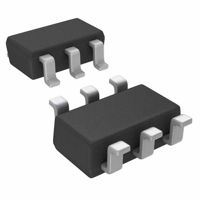
Packaging: 6Pin TSOT-26 & 8Pin DFN
SP6265
TSOT-26
Applications
•
•
•
•
Cellular Phones
Palm / Notebook
Battery Powered Equipment
Handheld Devices
TSOT-26
Top View
DESCRIPTION
The SP6265 dual, low dropout, linear regulators operate up to 5.5V input and deliver up to 150mA/150mA output
current per regulator. It has a bypass pin option which allows users to decouple the bandgap reference for reducing
the output noise. Low dropout voltage and low quiescent current (70µA typ.) make them ideal for battery powered
applications. The SP6265 is available with a wide variety of standard voltage options and can be trimmed to 1.5% accuracy. For protection purposes, SP6265 has a thermnal shutdown feature to prevent device failure under the"worst"
operating conditions.
TYPICAL APPLICATION CIRCUITS
SP6265 with Bypass
SP6265 without Bypass
VOUT1
VIN
VIN
EN1
SP6265
EN2
1µF
Aug17-07 Rev S
GND
VOUT1
VIN
VIN
SP6265
V OUT2
BYP
VOUT2
1µF
1µ F
1µF
SP6265 Dual Low-Dropout CMOS Voltage Regulator
�
V OUT1
EN
10nF
GND
VOUT1
VOUT2
V OUT2
1µF
1µ F
© 2007 Sipex Corporation
�ABSOLUTE MAXIMUM RATINGS
These are stress ratings only and functional operation of the device at these ratings or any other above those indicated in the operation sections of the specifications below is not implied.
Exposure to absolute maximum rating conditions for extended periods of time may affect reliability.
Thermal Resistance θJC
TSOT 26...........................................................................................81°C/W
DFN-8..............................................................................................17°C/W
Thermal Resistance θJA
TSOT 26..........................................................................................260°C/W
DFN-8.............................................................................................125°C/W
Internal Power Dissapation Pd
TSOT 26............................................................................................400mW
DFN-8...............................................................................................125mW
Input Voltage..................................................................................................6V
Output Current.....................................................Pd / [2Vin - (Vout1+Vout2)]mA
Output Voltage..................................................................GND- 0.3 to Vin+0.3V
ESD Classification......................................................................HBM C:4000V+
Ambient Temperature Range (Ta).................................................-40°C to 85°C
Junction Temperature Range (Tj) .................................................-40°C to 85°C
Lead Temperature (Soldering, 10 sec) .....................................................350°C
Maximum Junction Temperature ...............................................................150°C
Electrical Specifications
ELECTRICAL SPECIFICATIONS
Unless specified: TJ=25OC, VIN=Higher VOUT+�V, IOUT�=IOUT2=�mA, CIN=COUT=�.0µF, VEN�=VEN2=VIN
Typical values are at TJ=25OC
Parameter
Symbol
Test Condition
Min
Typ
Max
Units
5.5
V
�60
µA
IN
Input Supply Voltage
VIN
Quiescent Current
IQ
Note�
70
OUT1, OUT2
IOUT=�mA
Output Voltage
VO
0mA
很抱歉,暂时无法提供与“SP6265GEK1-L/TR”相匹配的价格&库存,您可以联系我们找货
免费人工找货