Solved by
SP6652
TM
1A, High Efficiency, Fixed 1.4 MHz
Current Mode PWM Buck Regulator
Features
■ 1A Output Current
■ 1.4MHz Constant Frequency Operation
■ 97% Efficiency Possible
■ 0.5µA (Max.) Shutdown Current
■ Adjustable Output Voltage
■ No External FETs or Schottky Diode Required
■ Uses Small Value Inductors and Ceramic
Output Capacitors
■ Low Dropout Operation: 100% Duty Cycle
■ Soft Start and thermal Shutdown Protection
■ Easy Frequency Synchonization
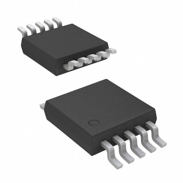
■ Lead Free, RoHS Compliant package: l
Small (3mm X 3mm) 10 Pin DFN or MSOP
10
LX
9
PVIN
8
S VIN
4
7
SYNC
5
6
MODE
PGND
1
SGND
2
FB
3
COMP
SD
SP6652
10 Pin DFN
applications
■ Mobile Phones
■ PDAs
■ DSCs
■ MP3 Players
■ USB Devices
■ Point of Use Power
DESCRIPTION
The SP6652 is a high efficiency, synchronous buck regulator ideal for portable applications
using one Li-Ion cell, with up to 1A of output current. The 1.4MHz switching frequency and
PWM control loop are optimized for a small value inductor and ceramic output capacitor,
for space constrained portable designs. In addition, the input voltage range of 2.7V to 5.5V;
excellent transient response, output accuracy, and ability to transition into 100% duty cycle
operation -- further extending useful battery life -- make the SP6652 a superior choice for
a wide range of portable power applications. A logic level shutdown control, external clock
synchronization, and forced-PWM or automatic control inputs are provided. Other features
include soft-start, over current protection and 140ºC over-temperature shutdown.
Typical Application CIRCUIT
VOUT
3.3V at 1A
4.7µH
1
2
340kΩ
LX
SGND
PVIN
9
SVIN
8
SYNC
7
MODE
6
3 FB
10µF
4
4kΩ
100kΩ
10
PGND
COMP
5 SD
SP6652
3.6V - 5.5V
VIN
10Ω
1µF
10µF
10nF
ENABLE
SHUTDOWN
Oct10-07 RevJ
SP6652 1A, High Efficiency, Current Mode PWM Buck Regulator
�
© 2007 Sipex Corporation
�ABSOLUTE MAXIMUM RATINGS
PVIN,SVIN ...........................................................................-0.3V to 6.0V
PGND to SGND .....................................................................-0.3V to 0.3V
LX to PGND ............................................................... - 0.3V to PVIN+0.3V
Storage Temperature.....................................................-65 °C to 150 °C
Operating Temperature................................................... -40°C to +85°C
These are stress ratings only and functional operation of the device at
these ratings or any other above those indicated in the operation sections of the specifications below is not implied. Exposure to absolute
maximum rating conditions for extended periods of time may affect
reliability.
Electrical CHARACTERISTICS
VIN = UVIN = VSDN = 3.6V, IO = 0mA, TAMB = -40°C to +85°C, typical values at 27°C unless otherwise noted.
The ♦ denotes the specifications which apply over the full temperature range, unless otherwise specified.
PARAMETER
MIN
TYP MAX UNITS
V
♦
0.816
V
♦
1
µA
4
%
♦
♦
1.4
1.6
MHz
180
230
ns
Input Operating Voltage
2.85
FB Set Voltage
0.784
0.8
FB Set Current
-1
0.01
Overall FB Accuracy
-4
Switching Frequency
1.2
Minimum On-Time-Duration
CONDITIONS
5.5
Result of IQ measurement at VIN = PVIN
= 5.5V
VFB = 0.8V
FB = COMP
Mode = SD = VIN
VFB = 1.0V, VCOMP = 0.2V
2.0
MHz
♦
0.01
1
µA
♦
0.3
0.6
V
♦
High to Low Transition
V
♦
Low to High Transition
PMOS Switch Resistance
0.4
0.6
Ω
♦
IPMOS = 200mA
NMOS Switch Resistance
0.4
0.6
Ω
♦
INMOS = 200mA
1.7
A
♦
VFB = 0.4V, Mode = SD = VIN
♦
SD = ZeroV
SYNC Tracking Frequency
1.0
SYNC Input Current
-1
SYNC Logic Threshold Low
SYNC Logic Threshold High
1.7
Mode = SD = VIN, VFB =1.0V
Inductor Current Limit
1.3
1.5
LX Leakage Current
-3
0.1
3
µA
1
5
mA
VIN = 3.6V, Mode = SD = VIN
3
10
mA
VIN = 5.5V, Mode = SD = VIN
2.7
2.85
V
VIN Quiecent Current
UVLO Undervoltage Lockout Threshold,
VIN falling
2.55
UVLO hysteresis
6
♦
SD = VIN
SD = VIN, VCOMP = 1V
%
Soft Start Current
1
2
4
µA
♦
SD MODE Input Current
-1
0.01
1
µA
♦
V
♦
♦
SD MODE Input Threshold Voltage
0.6
0.9
1.25
1.8
V
Slope Compensation
700
mA/µS
Rising Over-Temperature Trip Point
140
°C
Over-Temperature Hysteresis
14
°C
Error Amplifier Transconductance
1
mA/V
Oct10-07 RevJ
High to Low Transition
Low to High Transition
SP6652 1A, High Efficiency, Current Mode PWM Buck Regulator
�
© 2007 Sipex Corporation
�PIN DESCRIPTION
Pin
Number
PIN
NAME
DESCRIPTION
1
PGND
Power Ground Pin. Synchronous rectifier current returns through
this pin.
2
SGND
Internal Ground Pin. Control circuitry returns current to this pin.
3
FB
External feedback network input connection. Connect a resistor from
FB to ground and from FB to VOUT to control the output voltage.
Regulation point at FB = 0.8V Typical.
4
COMP
Compensation pin for error loop. Connect an R and C in series to
ground to control open loop pole and zero.
5
SD
Shutdown control input. Tie pin to VIN for normal operation, tie to
ground for shutdown. TTL input threshold.
6
MODE
Connect this pin to VIN.
7
SYNC
An external clock signal can be connected to this pin to synchronize
the switching frequency.
8
SVIN
Internal supply voltage. Control circuitry is powered from from this
pin. Use an RC filter close to the pin to cut down supply noise.
9
PVIN
Supply voltage for the output driver stage. Inductor charging current
passes through this pin.
10
LX
Inductor switching node. Inductor tied between this pin and the
output capacitor to create regulated output voltage.
PGND 1
S GND 2
10 LX
SP6652
FB 3
COMP 4
SD 5
Oct10-07 RevJ
10 Pin MSOP
PGND
1
10
LX
9 PVIN
SGND
2
9
PVIN
8 S VIN
FB
3
8
S VIN
COMP
4
7
SYNC
SD
5
6
MODE
7 SYNC
SP6652
10 Pin DFN
6 MODE
SP6652 1A, High Efficiency, Current Mode PWM Buck Regulator
�
© 2007 Sipex Corporation
�FUNCTIONAL Diagram
0.75V
0.3V
0.75V
REFOK
0.75V
0.75V
SD
Shutdown
VIN
+V
+V
Internal
Supply
2uA
SOFT
STRT
Q�
COMP
BLIM
R Qn
Q
SVIN
GO PWM
7.5mV PWM Mode Comparator
PWM/PFM
S
Soft Start
CHG
7.5mV PFM Loop Comparator
Error Amp
REFOK
Pre-amp
Gm
FB_LO
Inductor Current Clamp
CLAMP
PARK
PFM
PFM Node Park Clamp
A=3
DCHG
Low Vo Indicator
NOSWITCH
VREF
V0P3R
Reference
0.3V
FB
Charging
PMOS
Replica
300mA
M
Translator
A
R
S
RST
CHG
CLK
CLK
ILPK
CLR
Driver
+V
DCHG
+
+
Peak and Trough Current Detector
CNTR
S
R
Current Loop Comparator
GO PFM
PWM/PFM
- by �
Clock Generator
FB_LO
ILPK
Slope Compensation
CLR
OSC
SYNC
SYNC
Mode Select
PVIN
CLK
SOFT
STRT
GO PFM
GO PWM
Q�
MODE
LX
Changing
PMOS
100mA
LX
0mA
Internal
GND
SD
L�
PGND
SGND
Co
RL
VOUT
RF1
RF2
�
© 2007 Sipex Corporation
SP6652 1A, High Efficiency, Current Mode PWM Buck Regulator
Oct10-07 RevJ
�DETAILED DESCRIPTION
rent ramp times the resistance of the PMOS
charging switch. To keep the effective current
slope compensation constant (remembering
current is being compensated, not voltage)
the voltage slope must be proportional to
RPMOS. To account for this, the slope compensation voltage is internally generated
with a bias current that is also proportional
to RPMOS.
Current Mode Control and Slope
Compensation
The SP6652 is designed to use low value
ceramic capacitors and low value inductors
to reduce the converter’s volume and cost
in portable devices. Current mode PWM
control was, therefore, chosen for the ease
of compensation when using ceramic output
capacitors and better transient line rejection, which is important in battery powered
applications. Current mode control spreads
the two poles of the output power train filter
far apart so that the modulator gain crosses
over at -20dB/decade instead of the usual
-40dB/decade. The external compensation
network is, simply, a series RC circuit connected between ground and the output of the
internal transconductance error amplifier.
Over Current Protection
In steady state closed loop operation the
voltage at the COMP pin controls the duty
cycle. Due to the current mode control and the
slope compensation, this voltage will be:
V(COMP)•{ILPK•RPMOS + MCV•tON + VBE(Q1)}
It is well known that an unconditional instability exists for any fixed frequency currentmode converter operating above 50% duty
cycle. A simple, constant-slope compensation is chosen to achieve stability under these
conditions. The most common high duty
cycle application is a Li-Ion battery powered
regulator with a 3.3V output (D ≥ 90%). Since
the current loop is critically damped when the
compensation slope (denoted MCV) equals
the negative discharge slope (denoted M2V),
the amount of slope compensation chosen
is, therefore:
The COMP node will be clamped when its
voltage tries to exceed V(BLIM) + VBE(Q1).
The VBE(Q1) term is cancelled by VBE(Q2)
at the output of the translator. The correct
value of clamp voltage is, therefore:
V(BLIM) = IL(MAX)• RPMOS + MCV •TON
The IL(MAX) term is generated with a bias
current that is proportional to RPMOS, to
keep the value of current limit approximately
constant over process and temperature
variations, while the MCV •TON is generated
by a peak-holding circuit that senses the
amplitude of the slope compensation ramp
at the end of TON.
M2 = dIL/dTOFF =-Vout/L = -3.3V/4.7µH =
-702mA/µs
M2V = M2•RPMOS
There is minimum on-time (tON) generated
even if the COMP node is at zeroV, since
the peak current comparator is reset at the
end of a charge cycle and is held low during
a blanking time after the start of the next
charge cycle. This is necessary to swamp
the transients in the inductor current ramp
around switching times. The minimum tON
(100ns, nominally) is not sufficient for the
COMP node to keep control of the current
MCV = -M2V = 702mA/µs•0.2Ω = 140mV/µs,
for RPMOS = 0.20Ω
The inductor current is sensed as a voltage
across the PMOS charging switch and the
NMOS synchronous rectifier (see BLOCK
DIAGRAM). During inductor current charge,
V(PVIN)-V(LX) represents the charging curOct10-07 RevJ
SP6652 1A, High Efficiency, Current Mode PWM Buck Regulator
�
© 2007 Sipex Corporation
�DETAILED DESCRIPTION
when the output voltage is low. The inductor
current tends to rise until the energy loss
from the discharge resistances are equal to
the energy gained during the charge phase.
For this reason, the clock frequency is cut in
half when the feedback pin is below 0.3V, effectively reducing the minimum duty cycle in
half. Above V(FB) = 0.3V the clock frequency
is normal (see Typical Operating Characteristics: Inductor Current vs. VOUT)
The total power supply loop is compensated
with a series RC network connected from
the COMP pin to ground. Compensation is
simple due to current-mode control. The
modulator has two dominant poles: one at a
low frequency, and one above the crossover
frequency of the loop, as seen in the graph
below, Linearized Modulator Frequency
Response vs. Inductor Value.
The low frequency pole for L1= 5µH is
4kHz, the second pole is 500kHz, and the
gain-bandwidth is 20kHz. The total loop
crossover frequency is chosen to be 200kHz,
which is 1/6th of the clock frequency. This
sets the second modulator pole at 2.5 times
the crossover frequency. Therefore the gain
of the error amplifier can be 200kHz/20kHz
= 10 at the first modulator pole of 4kHz. The
error amp transconductance is 1mA/V, so
this sets the RZ resistor value in the compensation network at 10/1mA/V = 10kΩ.
The zero frequency is placed at the first
pole to provide at total system response of
-20dB/decade (the zero from the error amp
cancels the first modulator pole, leaving the
Voltage Loop and Compensation
in PWM Mode
The voltage loop section of the circuit consists of the error amplifier and the translator
circuits (see functional diagram). The input
of the voltage loop is the 0.8V reference voltage minus the divided down output voltage
at the feedback pin. The output of the error
amplifier is translated from a ground referred
signal (the COMP node) to a power input
voltage referred signal. The output of the
voltage loop is fed to the positive terminal
of the Current Loop comparator, and represents the peak inductor current necessary
to close the loop.
1 20K 2 2.0M 3 50K
16K
1.6M
40K
12K
1.2M
30K
8K
0.8M
20K
4K
0.4M
10K
0
0
>>
0
3u
2u
4u
5u
6u
1 Mod_pole12 Mod_pole2 3 Gbw_modfb
L1VAL
7u
8u
9u
10u
Conditions: VIN=5V, VOUT=3.3V, fCLK=1.4MHz, COUT=10µF, and MCV=132mV/µs. The inductor is varied from
2µH to 10µH
Linearized Modulator Frequency Response vs. Inductor
Oct10-07 RevJ
SP6652 1A, High Efficiency, Current Mode PWM Buck Regulator
�
© 2007 Sipex Corporation
�DETAILED DESCRIPTION
1 pole rolloff from the error amp pole). The
compensation capacitor becomes:
Cc =
1
(2π•Rz•pole1)
=
The switching frequency will be reduced to
half the normal frequency as long as V(FB)
is below 0.3V, as previously discussed in the
Over Current Protection section.
1
(6.28•10kΩ•4kHz)
= 4nF
100% Duty Cycle in Dropout
Soft Start
Soft-start is accomplished by disconnecting the error amp and inserting a constant
2μA current to charge the compensation
capacitor.
To extend the battery life in portable applications, the PWM control logic is set up such
that if the output SR latch has not been reset
by the Current Loop comparator at the end
of a clock cycle, the charge signal continues
to stay high into the beginning of the next
cycle. This will happen naturally when the
converter starts to go into dropout. The slope
compensation ramp is reset every cycle.
When power is first applied and the reference
establishes, the clamp circuit at the COMP
node sets its voltage at one VBE, which is
the bottom of the inductor current range. The
soft-start current continues to charge up the
COMP node, slowly raising the inductor current level. The inductor current will increase
at approximately:
External Clock Synchronization
(IREFSS / CC)• RPMOS
The SP6652 has an internal 1.4MHz clock
that can be defeated by connecting an external clock pulse on the SYNC. The capture
range for clock synchronization is 1.0 to
2.0MHz. When a clock pulse is present on
the SYNC pin, the internal oscillator bias
current is scaled back, handing control of
the clock pulses to the faster external clock.
The pulse width of the clock is approximately
50 ns, whether internally generated or externally applied.
where:
IREFSS = Soft start constant current
= 2μA nominally
C C
= Compensation capacitor
RPMOS = Charging PMOS resistance
For typical circuit values of CC=6.8nF and
RZ=8kΩ, the soft start period is TBD ms.
Thermal Shutdown
The inductor current will eventually rise
above the required load current and the output voltage will charge up. During soft-start
the error amp is disconnected and acts as
a comparator. When V(FB) rises above the
reference, the error amp switches to logic
high and ends soft-start, at which point the
error amp output is connected to the capacitated COMP node.
Oct10-07 RevJ
The internal die temperature is monitored by
a comparator that issues a “TOO HOT” signal when the junction temperature reaches
140˚C, nominally. This signal that inhibits
all internal circuits until the temperature
has decreased to approximately 135˚C, at
which point a normal soft start sequence is
initiated.
SP6652 1A, High Efficiency, Current Mode PWM Buck Regulator
�
© 2007 Sipex Corporation
�APPLICATIONS INFORMATION
L1
VOUT
4.7µH
R
C3
10µF
1 PGND
2 SGND
FBH
RFBL
3 FB
4 COMP
Rz
4kΩ
5 SD
LX
PVIN
SVIN
SYNC
MODE
10
9
R1
8
10Ω
7
6
VIN
C2
1µF
C1
10µF
SP6652
Cc
10nF
SD
VIN
Complete Application Circuit.
SYNC
Component Selection
The SP6652 PWM buck regulator circuit
requires 3 capacitors: 10µF for the PVIN input,
1µF input bypass for the SVIN and 10µF
for the output are typically recommended.
For the input capacitor, a value even larger
than 10µF will help reduce input voltage
ripple for applications sensitive to ripple on
the battery voltage. See the Typical Performance Characteristics section for waveforms on input and output ripple with 10µF
capacitors. All the capacitors should be
surface mount ceramic for low lead inductance necessary at the 1.4MHz switching
frequency of the SP6652 and to obtain low
ESR. This also helps improve bypassing
on the input pin and ripple on the output.
Ceramic capacitors with X5R or X7R temperature grade are recommended for most
applications. A selection of recommended
capacitors is included in Table 1. The 1µF
SVIN input capacitor should have a series
resistor of about 10Ω value connected
from the input to the SVIN pin to form an RC
low pass filter to remove high frequency
spikes present on the input switching pin
Oct10-07 RevJ
PVIN. This will keep the SP6652 internal
reference and other sensitive circuits noise
free and ensure better output regulation.
The GND returns for the PVIN capacitor and
the output capacitor should be connected
directly to the PGND pin, which should connect to the thermal pad ground located under the SP6652. The GND return for the
1µF SVIN capacitor should be connected to
the SGND pin, which should be connected
separately to the PGND pin to avoid adding
PGND noise to the SP6652 SGND pin. See
the Typical SP6652 Circuit Layout for details on the recommended layout.
Output Voltage Selection
To set the output voltage for the SP6652,
a pair of resistors, RF and RI are used as a
voltage divider between the output voltage
at the output capacitor and the FB pin and
GND, as shown in the typical application circuit. The recommended value for the RI resistor is 100KΩ to 200KΩ to keep the quiescent current low, but not have the impedance
too high at the FB pin for good regulation.
SP6652 1A, High Efficiency, Current Mode PWM Buck Regulator
�
© 2007 Sipex Corporation
�APPLICATIONS INFORMATION
Manufacturers/ Website
Part Number
TDK/www.tdk.com
TDK/www.tdk.com
TDK/www.tdk.com
Murata/www.murata.com
Murata/www.murata.com
Murata/www.murata.com
Capacitance/
Voltage
C1005X5R0J105M
C1608X5R0J475K
C2012X5R0J106M
GRM155R60J105KE19B
GRM188R60J475KE19
GRM21BR60J106KE19L
Table 1. Capacitor Selection
Capacitor
Size/Type/Thickness
1uF/6.3V
4.7uF/6.3V
10uF/6.3V
1uF/6.3V
4.7uF/6.3V
10uF/6.3V
ESR at
100KHz
0402/X5R/0.5mm
0603/X5R/0.9mm
0805/X5R/1.35mm
0402/X5R/0.55mm
0603/X5R/0.9mm
0805/X5R/1.35mm
0.03
0.02
0.02
0.03
0.02
0.02
Note: Component highlighted in bold is used on the SP6652EB Evaluation Board.
The range of typical inductor values and sizes are shown here in Table 2.
Manufacturers/ Website
Part Number
Inductance/ Isat
Rating
Coilcraft/ www.coilcraft
Coilcraft/ www.coilcraft
Sumida/ www.sumida.com
Sumida/ www.sumida.com
Wurth Elektronik/ www.we-online.de
Wurth Elektronik/ www.we-online.de
MSS5131-332MX
MSS5131-332MX
CDRH3D28-3R3
CDRH3D28-4R7
WE-TPC #744042003
WE-TPC #744042004
3.3uH/1.6A
4.7uH/1.4A
3.3uH/2.0A
4.7uH/1.65A
3.3uH/1.8A
4.7uH/1.65A
Table 2. Inductor Selection
DCR Max
ohms
5.1x5.1x3.1mm
5.1x5.1x3.1mm
4.0x4.0x3.0mm
4.0x4.0x3.0mm
4.8/4.8/1.8mm
4.8/4.8/1.8mm
0.032
0.045
0.058
0.071
0.065
0.082
Note: Component highlighted in bold is used on the SP6652EB Evaluation Board.
SP6652 Bode Plot
The output voltage can be set using the
formula:
VOUT = VFB*(1 + RF/RI)
60
50
40
30
20
10
0
-10
-20
-30
-40
-50
-60
100
Where VFB = 0.8V typically, and for no-load
Ton is kept within 200nsec Minimum:
Ton(min) = VOUT/(VIN *Freq).
Compensation Component Selection
For simplicity in compensation with ceramic output capacitors, the SP6652 uses
current mode PWM control, so all that is
needed for stability is a series RZ and CC
at the COMP pin to compensate the error
amplifier. To see the actual SP6652 response with frequency, in figure 3 we have
taken a bode plot of gain and frequency response of the SP6652 circuit with 3.3Vout.
Looking first at the SP6652 Modulator Gain
at low frequency you see a constant gain
of about 26dB and the first pole or -3dB
point at about 4 kHz, where the slope of
the gain curve becomes about -20dB/decade. At high frequency on the SP6652
Modulator Gain curve one can see the
modulator curve slope increase downOct10-07 RevJ
Inductor
Length/Width/Thickness
.
At 0dB Loop Gain
Fo = 80kHz
Loop Phase = 50deg
pole1 -3dB
at 4kHz
-20dB/dec
3.3Vout
Rz = 4K Ω
Cc = 10nF
1000
10000
SP6652 Loop Gain
SP6652 Modulator Gain
SP6652 Loop Phase
SP6652 Modulator Phase
100000
180
150
120
90
60
30
0
-30
-60
-90
-120
-150
-180
1000000
Log
Frequency (Hz)
Figure 3. SP6652 Gain and Frequency
Response 3.3V output voltage
ward for a high frequency pole at about
150KHz, which is widely separated in
frequency from the low frequency 4kHz
pole, so that the SP6652 can be compensated by a zero at the low frequency pole
where the gain slope is only -20dB/decade.
The gain for the error amplifier is the cross-
SP6652 1A, High Efficiency, Current Mode PWM Buck Regulator
�
© 2007 Sipex Corporation
�APPLICATIONS INFORMATION
The zero for loop compensation is placed
at the first modulator pole of 4 kHz to provide a loop response of -20/dB/decade at
the crossover frequency. The compensation capacitor Cc can be calculated from
the crossover frequency pole1 and the RZ
value:
over frequency fzero = 80kHz (from the
Bode plot) divided by the loop gain bandwidth, given as 20kHz, which is used in the
following equation:
Error Amp Gain
= fzero / (loop gain bandwidth)
= 80kHz / 20kHz
=4
CC = 1/(2π• RZ •pole1) = 1/(2π•4K•4kHz)
= 10nF
The error amp transconductance is about
1mS, so this sets the RZ resistor to be:
From the Typical Performance Characteristics load step curves, the 2.5V output
and 3.3V output are stable with RZ = 4KΩ
and CC = 10nF. For 1.8V to 0.85V output,
the values RZ = 2KΩ and CC = 10nF are
recommended.
Rz = 4/1mS = 4KΩ
We will use RZ = 4KΩ for the 3.3V output
compensation.
Figure 4. Typical SP6652 circuit layout.
Oct10-07 RevJ
SP6652 1A, High Efficiency, Current Mode PWM Buck Regulator
10
© 2007 Sipex Corporation
�TYPICAL PERFORMANCE CHARACTERISTICS
SP6652 Efficiency vs Load Vout = 3.3V
SP6652 Efficiency vs Load (Vout = 1.5V)
100
100
.(
90
90
80
70
70
Efficiency (%)
80
60
50
Vi=3.6V
40
Vi=3.9V
30
Vi=4.2V
20
60
50
Vi=3.9V
20
10
10
0
0
10
Vi=3.6V
30
Vi=5.0V
1
Vi=3.0V
40
100
Vi=4.2V
1
1000
10
100
Figure 6. Efficiency vs. Load, Vout= 1.5V
Figure 5. Efficiency vs. Load, Vout= 3.3V
SP6652 Line/Load Rejection Vout = 3.3V
3.40
1000
ILoad (mA)
ILoad (mA)
SP6652 Line/Load Rejection VOUT = 1.5V
. (V
1.520
3.35
1.510
3.30
1.500
VOUT (V)
Vi=3.6V
Vi=3.9V
3.25
Vi=4.2V
Vi=4.2V
Vi=3.9V
1.490
Vi=3.6V
Vi=3.0V
Vi=5.0V
1.480
3.20
0
200
400
600
800
1000
0
200
400
ILoad (mA)
800
1000
Figure 8: Line/Load Rejection , Vout = 1.5V
Figure 7: Line/Load Rejection , Vout = 3.3V
SP6652 Line/Load Regulation, Vout = 3.3V
3.340
600
ILoad (mA)
SP6652 Line/Load Rejection VOUT = 1.5V
1.520
.(V
3.330
1.510
3.320
3.310
VOUT (V)
1.500
Vi=3.6V
3.300
Vi=3.9V
Vi=4.2V
3.290
Vi=4.2V
Vi=3.9V
1.490
Vi=3.6V
Vi=5.0V
Vi=3.0V
1.480
3.280
1
10
100
1000
1
ILoad (mA)
100
1000
ILoad (mA)
Figure 10: Line/Load Regulation , Log Scale,
Vout = 1.5V
Figure 9: Line/Load Regulation , Log Scale,
Vout = 3.3V
Oct10-07 RevJ
10
SP6652 1A, High Efficiency, Current Mode PWM Buck Regulator
11
© 2007 Sipex Corporation
�TYPICAL PERFORMANCE CHARACTERISTICS
Figure 11. 0mA to 600mA
Load Step Data
Vin=4.2V, Vo=3.3V
Rz=4kW, Cz=10nF, L1=4.7uH
Vo(AC)
200mV/div
IL1
(0.5A/div)
Figure 12. 0mA to 600mA
Load Step Data
Vin=4.2V, Vo=1.5V
Rz=2kW, Cz=10nF,
L1=4.7uH
Iout
(1.0A/div)
Vo(AC)
200mV/div
IL1
(0.5A/div)
Iout
(0.5A/div)
Oct10-07 RevJ
Figure 13. 0mA to 600mA
Load Step Data
Vin=4.2V, Vo=2.5V
Rz=4kW, Cz=10nF,
L1=4.7uH
SP6652 1A, High Efficiency, Current Mode PWM Buck Regulator
12
© 2007 Sipex Corporation
�TYPICAL PERFORMANCE CHARACTERISTICS
EN
Vout
Figure 14. SP6652 600mA
Start-up from Enable
Vin=4.2V, Vo=3.3V, Iout =
600mA, Rz=4kW, Cz=10nF,
ILX
0.5A/divL1=4.7uH
EN
Vout
Figure 15. SP6652 600mA
Start-up from Enable
Vin=4.2V, Vo=1.5V, Iout =
600mA, Rz=2kW, Cz=10nF,
L1=4.7uH
ILX
0.5A/div
Vin
(AC)
Figure 16. SP6652 600mA
Input/Output Ripple
Vin=4.2V, Vo=3.3V, Iout =
600mA, Rz=4kW, Cz=10nF,
L1=4.7uH
Vout
(AC)
Vin
(AC)
Vout
(AC)
Oct10-07 RevJ
Figure 17. SP6652 600mA
Input/Output Ripple
Vin=4.2V, Vo=1.5V, Iout =
600mA, Rz=2kW, Cz=10nF,
L1=4.7uH
SP6652 1A, High Efficiency, Current Mode PWM Buck Regulator
13
© 2007 Sipex Corporation
�PACKAGE: 10 PIN MSOP
Oct10-07 RevJ
SP6652 1A, High Efficiency, Current Mode PWM Buck Regulator
14
© 2007 Sipex Corporation
�PACKAGE: 3X3 10 PIN DFN
Oct10-07 RevJ
SP6652 1A, High Efficiency, Current Mode PWM Buck Regulator
15
© 2007 Sipex Corporation
�Ordering Information
Part Number
MSL Level
RoHS
SP6652ER-L
SP6652ER-L/TR
SP6652EU-L/TR
SP6652EU-L
SP6652ER
SP6652ER/TR
SP6652EU
SP6652EU-ES
SP6652EU/TR
L1 @ 260ºC
L1 @ 260ºC
L1 @ 260ºC
L1 @ 260ºC
L1 @ 240ºC
L1 @ 240ºC
L1 @ 240ºC
L1 @ 240ºC
L1 @ 240ºC
Yes
Yes
Yes
Yes
No
No
No
No
No
Min
Max Temp
Temp
-40
85
0
70
0
70
0
70
-40
85
-40
85
0
70
0
70
0
70
Package
Pack Type
Quantity
DFN10
DFN10
MSOP10
MSOP10
DFN10
DFN10
MSOP10
MSOP10
MSOP10
Canister
Tape & Reel
Tape & Reel
TUBE
Canister
Tape & Reel
TUBE
TUBE
Tape & Reel
Any
3000
2500
50
Any
3000
50
50
2500
Evaluation Boards
Not Available in
Not Applicable to
No
0
70
Board
Board
Bulk
Not Available in
Not Applicable to
SP6652LEDEB
No
0
70
Board
Board
Bulk
Note: The SP6652EB is for regular SP6652 users, the SP652LEDEB is for LED driver users.
SP6652EB
For latest information on ordering status, go to the Sipex Web Landing Page for this product
http://www.sipex.com/productDetails.aspx?part=SP6652&keyword=sp6652
For further assistance:
Email:
WWW Support page:
Sipex Application Notes:
Solved by
TM
Sipexsupport@sipex.com
http://www.sipex.com/content.aspx?p=support
http://www.sipex.com/applicationNotes.aspx
Sipex Corporation
Headquarters and
Sales Office
233 South Hillview Drive
Milpitas, CA 95035
tel: (408) 934-7500
fax: (408) 935-7600
Sipex Corporation reserves the right to make changes to any products described herein. Sipex does not
assume any liability arising out of the application or use of any product or circuit described herein; neither
does it convey any license under its patent rights nor the rights of others.
Oct10-07 RevJ
SP6652 1A, High Efficiency, Current Mode PWM Buck Regulator
16
© 2007 Sipex Corporation
�