S P X1 5 8 7
3A Low Dropout Voltage Regulator
September 2010
Rev. 2.0.0
GENERAL DESCRIPTION
APPLICATIONS
The SPX1587 is a low power positive-voltage
regulator designed to satisfy moderate power
requirements with a cost effective, small
footprint solution.
• Desktop PC's Servers
This device is an excellent choice for use in
battery-powered applications and portable
computers. The SPX1587 features very low
quiescent current and a low dropout voltage of
1.1V at a full load. As output current
decreases, quiescent current flows into the
load, increasing efficiency. SPX1587 is
available in adjustable or fixed 1.5V, 2.5V,
3.3V and 5.0V output voltages.
• Portable Instrumentation
The SPX1587 is offered in several 3-pin
surface mount packages: TO-252, TO-220 and
TO-263. An output capacitor of 10μF ceramic
or tantalum provides unconditional stability.
• Powering VGA and Sound Cards
• Adjustable Power Supplies
FEATURES
• Guaranteed 3A Output Current
• Three Terminal Adjustable or Fixed
1.5V, 2.5V, 3.3V and 5.0V
• Low Quiescent Current
• Low Dropout Voltage: 1.1V at 3A
• Line Regulation: 0.1%
• Load Regulation: 0.1%
• Stable with 10uF Ceramic Capacitor
• Over Current and Thermal Protection
• Similar to Industry Standard
LT1085/LT1585
• RoHS Compliant Lead Free 3-Pin
TO-220, TO-252 and TO-263 Packages
FUNCTIONAL DIAGRAM
Fig. 1: SPX1587 Functional Diagram (Adjustable version)
Exar Corporation
48720 Kato Road, Fremont CA 94538, USA
www.exar.com
Tel. +1 510 668-7000 – Fax. +1 510 668-7001
�S P X1 5 8 7
3A Low Dropout Voltage Regulator
ABSOLUTE MAXIMUM RATINGS
OPERATING RATINGS
These are stress ratings only and functional operation of
the device at these ratings or any other above those
indicated in the operation sections of the specifications
below is not implied. Exposure to absolute maximum
rating conditions for extended periods of time may affect
reliability.
Junction Temperature Range ....................-40°C to 125°C
Thermal Resistance
TO-220 θJC ...................................................... 3°C/W
TO-220 θJA ................................................. 29.4°C/W
TO-263 θJC ...................................................... 3°C/W
TO-263 θJA ................................................. 31.4°C/W
TO-252 θJC ...................................................... 6°C/W
TO-252 θJA .................................................... 50°C/W
Input Supply Voltage VIN .................................... +10.0V
Input to Output Voltage ....................................... +8.8V
Storage Temperature .............................. -65°C to 150°C
Power Dissipation ................................ Internally Limited
Lead Temperature (Soldering, 5 sec) ..................... 260°C
ESD Rating (HBM - Human Body Model) .................... 2kV
ELECTRICAL SPECIFICATIONS
Specifications with standard type are for an Operating Ambient Temperature of TA = 25°C only; limits applying over the full
Operating Temperature range (-40°C to +85°C) are denoted by a “•”. Minimum and Maximum limits are guaranteed
through test, design, or statistical correlation. Typical values represent the most likely parametric norm at TA = 25°C, and
are provided for reference purposes only. Unless otherwise indicated, VIN = VOUT + 1.5V, TA = 25°C, CIN = COUT =10µF,
IOUT=10mA.
Parameter
Min.
Typ.
1.485
1.500
Max.
Units
Conditions
1.5V Version
Output Voltage
SPX1587A
1.515
1.530
1.470
V
IOUT=10mA, VOUT=3.5V
•
10mA≤IOUT≤3A, 3.0V≤VOUT≤10V
•
10mA≤IOUT≤3A, 4.25V≤IOUT≤10V
•
10mA≤IOUT≤3A, 4.75V≤VOUT≤10V
•
10mA≤IOUT≤3A, 4.75V≤VOUT≤10V
•
10mA≤IOUT≤3A, 6.50V≤VOUT≤10V
•
10mA≤IOUT≤3A, 1.50V≤VIN-VOUT≤10V
•
10mA≤IOUT≤3A, 1.50V≤VIN-VOUT≤10V
2.5V Version
Output Voltage
SPX1587
2.450
2.500
2.550
2.575
2.425
V
IOUT=10mA, VOUT=4.5V
3.3V Version
3.267
Output Voltage
SPX1587A
3.234
Output Voltage
SPX1587
3.201
3.234
3.300
3.333
3.366
3.300
3.366
3.399
V
V
IOUT=10mA, VOUT=5V
IOUT=10mA, VOUT=5V
5.0V Version
Output Voltage
SPX1587A
4.950
5.000
5.050
5.100
4.900
V
IOUT=10mA, VOUT=7V
All Voltage Options
1.238
Reference Voltage
SPX1587A
1.225
Reference Voltage
SPX1587
1.212
1.225
1.250
1.262
1.275
1.250
1.275
1.287
V
V
Output Voltage Temperature
Stability – SPX1587A
0.3
%
Output Voltage Temperature
Stability – SPX1587
0.5
%
IOUT=10mA, VIN-VOUT=2V
IOUT=10mA, VIN-VOUT=2V
3.0V≤VIN≤10V, VOUT=1.5V
Line Regulation
0.1
0.2
%
4.25V≤VIN≤10V, VOUT=2.5V
4.75V≤VIN≤10V, VOUT=3.3V
6.50V≤VIN≤10V, VOUT=5.0V
10mA≤IOUT≤3A, VOUT=1.5V
Load Regulation
0.1
0.3
%
10mA≤IOUT≤3A, VOUT=2.5V
10mA≤IOUT≤3A, VOUT=3.3V
10mA≤IOUT≤3A, VOUT=5.0V
© 2010 Exar Corporation
2/11
Rev. 2.0.0
�S P X1 5 8 7
3A Low Dropout Voltage Regulator
Parameter
Min.
Typ.
Max.
Units
Conditions
IOUT=1A
1.00
Dropout Voltage (note 2)
Minimum Load Current
(note 4)
Quiescent Current
Current Limit
1.2
4
10
mA
4
10
mA
5
0.01
Fixed Voltage Versions
µA
120
3.2
Thermal Regulation
Ripple Rejection
IOUT=3A
1.10
50
Adjust Pin Current
IOUT=2A
V
1.05
µA
•
A
0.1
%/W
VIN-VOUT=2V
25°C, 30ms pulse
75
dB
FRIPPLE=120Hz, VIN-VOUT=2V, VRIPPLE=1VPP
Long Term Stability
0.03
%
125°C, 1000 hours
RMS Output Noise
0.03
%
% of VOUT, 10Hz ≤ f ≤ 10kHz
60
Note 1: Output temperature coefficient is defined as the worst case voltage change divided by the total temperature range
Note 2: Dropout voltage is defined as the input to output differential at which the output voltage drops 100mV below its
nominal value measured at 1V differential at very low values of programmed output voltage, the minimum input supply
voltage of 2V (2.3V over temperature) must be taken into account.
Note 3: Thermal regulation is defined as the change in output voltage at a time T after a change in power dissipation is
applied. Excluding load or line regulation effect.
Note 4: Adjustable Version Only.
BLOCK DIAGRAM
Fig. 2: SPX1587 Block Diagram
© 2010 Exar Corporation
3/11
Rev. 2.0.0
�S P X1 5 8 7
3A Low Dropout Voltage Regulator
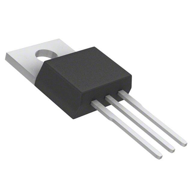
PIN ASSIGNMENT
Fig. 3: SPX1587 Pin Assignment
PIN DESCRIPTION
Name
Pin Number
ADJ/GND
1
Description
Adjustable Voltage Pin or Ground signal for fixed voltage versions.
VOUT
2
Output Voltage
VIN
3
Input Voltage
TAB
TAB
Tab is connected to VOUT (pin 2) for all packages
ORDERING INFORMATION
Part Number
SPX1587T-L
SPX1587T-L/TR
SPX1587T-L-1-5
SPX1587T-L-1-5/TR
SPX1587T-L-5-0
SPX1587T-L-5-0/TR
Junction
Temperature Range
-40°C≤TJ≤+125°C
-40°C≤TJ≤+125°C
-40°C≤TJ≤+125°C
SPX1587U-L-3-3
-40°C≤TJ≤+125°C
SPX1587U-L-5-0
-40°C≤TJ≤+125°C
SPX1587AR-L
SPX1587AR-L/TR
SPX1587AT-L
SPX1587AT-L/TR
SPX1587AT-L-2-5
SPX1587AT-L-2-5/TR
SPX1587AT-L-3-3
SPX1587AT-L-3-3/TR
SPX1587AU-L
-40°C≤TJ≤+125°C
-40°C≤TJ≤+125°C
-40°C≤TJ≤+125°C
-40°C≤TJ≤+125°C
-40°C≤TJ≤+125°C
Marking
Sipex
SPX1587T
YYWWLX
Sipex
SPX1587T
15YYWWLX
Sipex
SPX1587T
50YYWWLX
Sipex
SPX1587U
33YYWWLX
Sipex
SPX1587U
50YYWWLX
Sipex
SPX1587AR
YYWWLX
Sipex
SPX1587AT
YYWWLX
Sipex
SPX1587AT
25YYWWLX
Sipex
SPX1587AT
33YYWWLX
Sipex
SPX1587AU
YYWWLX
Package
TO263-3
TO263-3
TO263-3
Packing Quantity
Bulk
500/Tape & Reel
Bulk
500/Tape & Reel
Bulk
500/Tape & Reel
Note 1
Lead Free
Lead Free
Lead Free
TO220-3
Bulk
Lead Free
TO220-3
Bulk
Lead Free
TO252-3
TO263-3
TO263-3
TO263-3
TO220-3
Bulk
2K/Tape & Reel
Bulk
500/Tape & Reel
Bulk
500/Tape & Reel
Bulk
500/Tape & Reel
Bulk
Lead Free
Lead Free
Lead Free
Lead Free
Lead Free
“YY” = Year – “WW” = Work Week – “L” = Lead Free Indicator – “X” = Lot Number; when applicable.
© 2010 Exar Corporation
4/11
Rev. 2.0.0
�S P X1 5 8 7
3A Low Dropout Voltage Regulator
TYPICAL PERFORMANCE CHARACTERISTICS
All data taken at VIN = VOUT + 1.5V, TA = 25°C, CIN = COUT =10µF, IOUT=10mA unless otherwise specified - Schematic and
BOM from Application Information section of this datasheet.
Fig. 4: Line Regulation for SPX1587U-3-3
IOUT=10mA
Fig. 5: VOUT versus Temperature
VIN=2.5V, IOUT=10mA
Fig. 6: VOUT versus Temperature
VIN=4.0V, IOUT=10mA
Fig. 7: VOUT versus Temperature
VIN=5.0V, IOUT=10mA
SOLDERING METHODS
APPLICATION INFORMATION
The SPX1587 die is attached to the heatsink
lead which exits opposite the input, output,
and ground pins.
OUTPUT CAPACITOR
To ensure the stability of the SPX1587, an
output capacitor of at least 10μF (ceramic or
tantalum) or 22μF (aluminum) is required. The
value may change based on the application
requirements
of
the
output
load
or
temperature range. The value of ESR can vary
based on the type of capacitor used in the
applications to guarantee stability. The
recommended value for ESR is 0.5Ω or less. A
larger value of output capacitance (up to
100μF) can improve the load transient
response.
© 2010 Exar Corporation
THERMAL CHARACTERISTICS
The SPX1587 features the internal thermal
limiting to protect the device during overload
conditions. Special care needs to be taken
during continuous load conditions such that
the maximum junction temperature does not
exceed 125°C. Thermal protection is activated
at >179°C and deactivated at