XR21B1424
Enhanced 4-Ch Full-Speed USB UART
General Description
FEATURES
The XR21B1424 is an enhanced Universal Asynchronous Receiver and
Transmitter (UART) bridge to USB interface. The USB interface is fully
compliant to the USB 2.0 (Full-Speed) specification with 12 Mbps USB
data transfer rate. The USB interface also supports USB suspend,
resume and remote wakeup operations. The USB Vendor ID, Product ID,
power mode, remote wakeup support, maximum power, and numerous
other settings may be programmed in the on-chip OTP memory via the
USB interface.
• ±15kV ESD on USBD+/USBD• USB 2.0 Compliant, Full-Speed (12Mbps)
• Unique pre-programmed USB serial number
• Internally generated 48MHz core clock
• Enhanced UART features
• Baud rates from 300 bps to 12 Mbps
• Fractional Baud Rate Generator
• 512-byte TX and 512-byte RX FIFOs
• Auto Hardware / Software Flow Control
• Multidrop and Half-Duplex Modes
• Auto RS-485 Half-Duplex Control
• Selectable GPIO or Modem I/O
• Up to 10 GPIOs per channel
• 5V tolerant GPIO inputs
• Suspend state GPIO configuration
• Configurable clock output
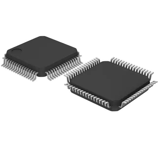
• 64-pin LQFP package
The XR21B1424 includes an internal oscillator and does not require an
external crystal/oscillator. Any UART baud rate from 300 bps to 12 Mbps
may be generated with this internal clock and the fractional baud rate generator.
The UART pins for each port may also be configured as GPIO; direction,
state, output driver type and input pull-up or pull-down resistors are programmed either through on chip OTP, or on the fly via memory mapped
registers.
Large 512-byte TX and RX FIFOs prevent buffer overflow errors and optimize data throughput. Automatic half-duplex direction control and optional
multi drop (9-bit) mode simplify both hardware and software in half-duplex
RS-485 applications. Wide mode allows for each individual received character to be monitored for errors.
The XR21B1424 uses the native OS CDC-ACM driver or a MaxLinear
supplied custom driver. MaxLinear provides WHQL/HCK-certified software drivers for Windows 2000, XP, Vista, 7, 8, 8.1 and 10 as well as software drivers for Windows CE, Linux and Mac OS X. Full source code is
available.
The XR21B1424 operates from a single 5V or 3.3V power supply. When
powered with 5V input, a regulated 3.3V output is supplied.
• Industrial -40°C to +85°C Temperature
Range
APPLICATIONS
• Building Automation
• Security Systems
• Factory and Process Control
• ATM Terminals
• USB to Serial Controllers
Ordering Information – page 64
Typical Application
XR21B1424
MCU
USB
0D[/LQHDU
UART
�
�
'DWD
1 / 66
�
�
��ESV�
exar.com/XR21B1424
Rev 1E
�XR21B1424
Absolute Maximum Ratings
Operating Conditions
Stresses beyond those listed under Absolute Maximum
Ratings may cause permanent damage to the device.
Exposure to any Maximum Rating may affect device
reliability and lifetime.
Operating Temperature Range.....................-40°C to +85°C
Supply Voltage (VCC_REG)......................................+5.75V
Supply Voltage (VCC, VIO)............................................+4V
Input Voltage (VBUS_SENSE).......................-0.3 to +5.75V
Input Voltage (All other pins)............................-0.3 to +5.6V
Junction Temperature.................................................125°C
Electrical Characteristics
Unless otherwise noted: TA = -40°C to +85°C, VCC_REG = +4.4V to +5.25V or +3.0V to +3.6V, VIO = +1.8V to +3.6V.
Symbol
Parameter
Conditions
Min
Typ
Max
Units
15
23
mA
0.85
1.25
mA
3.3
3.6
V
Power
ICC
Power Supply Current
ISUSP
Lowpower Mode Current
VOUT
Regulated Output Voltage (VCC pin)
VCC_REG = +4.4V to +5.25V
VCC_REG = +4.4V to +5.25V.
Maximum output current = 200 mA including
the supply current of the XR21B1424.
3
UART, USB_STAT and GPIO Pins
VIL
Input Low Voltage
-0.3
0.25*
VIO
V
VIH
Input High Voltage
0.70*
VIO
5.5
V
VOL
Output Low Voltage
IOL = 1mA, VIO = +1.6V
0.3
V
IOL = 4mA, VIO = +3.6V
0.5
V
VOH
Output High Voltage
IOH = -400uA, VIO = +1.6V
1.3
VIO
V
IOH = -1.5mA, VIO = +3.6V
2.8
VIO
V
IIL
Input Low Leakage Current
VIO = +3V to +3.6V, VCC_REG = +4.4V to
+5.25V, VINPUT = 0V
±10
µA
IIH
Input High Leakage Current
VIO = +3V to +3.6V, VCC_REG = +4.4V to
+5.25V, VINPUT = +3.3V
±10
µA
VIO = +3V to +3.6V, VCC_REG = +4.4V to
+5.25V, VINPUT = +5.5V
±120
µA
5
pF
CIN
Input Pin Capacitance
2 / 66
exar.com/XR21B1424
Rev 1E
�XR21B1424
Symbol
Parameter
Conditions
Min
Typ
Max
Units
USB I/O Pins
VIL
Input Low Voltage
-0.3
0.8
V
VIH
Input High Voltage
2.0
5.5
V
VOL
Output Low Voltage
External 15kΩ to GND on USBD+ and
USBD- pins
0
0.3
V
VOH
Output High Voltage
External 15kΩ to GND on USBD+ and
USBD- pins
2.8
3.6
V
VDrvZ
Driver Output Impedance
28
44
Ω
3 / 66
exar.com/XR21B1424
Rev 1E
�XR21B1424
GPIOD6/CLKD
GPIOD7/RS485D
GPIOD8/TXTD
50
49
TXD
52
51
GPIOD5/RTSD#/RS485D
RXD
53
GPIOD4/CTSD#
55
54
GPIOD2/DSRD#
GPIOD3/DTRD#
56
GPIOD1/CDD#
57
GPIOD0/RID#/RWKD#
59
GPIOA8/TXTA
GPIOA9/RXTA
60
58
GPIOA7/RS485A
62
61
TXA
64
63 GPIOA6/CLKA
Pin Configuration
RXA
1
48
GPIOD9/RXTD
GPIOA5/RTSA#/RS485A
2
47
GPIOB0/RIB#/RWKB#
GPIOA4/CTSA#
3
46
GPIOB1/CDB#
GPIOA3/DTRA#
4
45
GPIOB2/DSRB#
GPIOA2/DSRA#
5
44
GPIOB3/DTRB#
GPIOA1/CDA#
6
43
GPIOB4/CTSB#
GPIOA0/RIA#/RWKA#
7
42
GPIOB5/RTSB#/RS485B
MaxLinear
XR21B1424
29
30
31
32
GPIOC3/DTRC#
GPIOC1/CDC#
TEST#
GPIOC0/RIC#/RWKC#
GPIOC2/DSRC#
GPIOB9/RXTB
33
28
34
16
GPIOC4/CTSC#
15
27
NC
VBUS_SENSE
26
GPIOB8/TXTB
RXC
35
GPIOC5/RTSC#/RS485C
14
25
NC
USB_STAT1
GPIOB7/RS485B
24
36
TXC
13
23
GPIOB6/CLKB#
VCC_REG
22
37
GPIOC6/CLKC
12
GPIOC7/RS485C
VIO
VCC
21
38
NC
11
19
GND
VIO
20
39
GPIOC8/TXTC
10
GPIOC9/RXTC
TXB
USBD-
17
RXB
40
18
41
9
RESET#
8
USB_STAT2
GND
USBD+
Top View
4 / 66
exar.com/XR21B1424
Rev 1E
�XR21B1424
Pin Assignments
Pin No.
Pin Name
Type
I
Description
1
RXA
2
GPIOA5/RTSA#/RS485A
I/O
General purpose I/O, or UART Request-to-Send output (active low), or auto RS-485 halfduplex control. Defaults to GPIO input with internal pull-up resistor. See “Automatic RTS/CTS
Hardware Flow Control” on page 16 or “Multidrop mode with address matching” on page 18.
3
GPIOA4/CTSA#
I/O
General purpose I/O, or UART Clear-to-Send input (active low). Defaults to GPIO input with
internal pull-up resistor. See “Automatic RTS/CTS Hardware Flow Control” on page 16.
4
GPIOA3/DTRA#
I/O
General purpose I/O, or UART Data-Terminal-Ready push-pull output (active low). Defaults to
GPIO input with internal pull-up resistor. See “Automatic DTR/DSR Hardware Flow Control” on
page 17.
5
GPIOA2/DSRA#
I/O
General purpose I/O, or UART Data-Set-Ready input (active low). Defaults to GPIO input with
internal pull-up resistor. See “Automatic DTR/DSR Hardware Flow Control” on page 17.
6
GPIOA1/CDA#
I/O
General purpose I/O, or UART Carrier-Detect input (active low). Defaults to GPIO input with
internal pull-up resistor.
7
GPIOA0/RIA#/RWKA#
I/O
General purpose I/O, or UART Ring-Indicator input (active low), or Remote Wakeup input.
Defaults to GPIO input with internal pull-up resistor. Wakeup signaling to the USB host is sent
when a falling edge is detected. See “Remote Wakeup” on page 10.
8
GND
9
USBD+
I/O
USB port differential data positive. This pin has internal pull-up resistor compliant to the USB
2.0 specification. The ESD protection on this pin is ±15kV HBM.
10
USBD-
I/O
USB port differential data negative. The ESD protection on this pin is ±15kV HBM.
11
VIO
PWR
I/O voltage input to the UART/GPIO pins. Must be between 1.8 and 3.6V. May be connected to
VCC (pin 12) if VCC_REG input voltage is 5V. See “USB Power Modes” on page 12.
12
VCC
PWR
3.3V power to the device, or 3.3V power output from the device when 5V power is supplied to
VCC_REG pin. 3.3V output power can source up to 200 mA maximum (including the device)
and should be decoupled by minimum of 4.7µF ceramic capacitor. See “USB Power Modes”
on page 12.
13
VCC_REG
PWR
5V or 3.3V power to the device. In bus-powered mode, connect VBUS power from the USB
host to this pin and to the VBUS_SENSE pin - see Figure 1. To conform to USB specifications,
an inrush current limiting circuit is recommended. In self-powered mode, connect on-board 5V
or 3.3V source to this pin and VBUS from the USB host to the VBUS_SENSE pin. See
Figure 2 and Figure 3. USB specification requires a minimum of 1uF and a maximum of 10uF
of decoupling on VBUS power.
14
NC
-
No Connect.
15
NC
-
No Connect.
16
VBUS_SENSE
I
Must be connected to VBUS power from the USB host PC. This pin is used to disable the internal pull-up resistor on the USBD+ signal when VBUS is not present. In bus-powered mode,
connect VBUS (5V) power from the USB host to this pin and to the VCC_REG pin - see Figure
1. In self-powered mode, connect VBUS from the USB host to this pin. This pin must be
decoupled by a 4.7 uF tantalum capacitor.
17
RESET#
I/O / OD
Active low open drain output. Asserted at power on or any time device is reset by either register or USB bus reset. As an input, must be asserted for at least 15µs to force a device reset.
Reset pulse width input of shorter than 15µs will have unknown effects. A weak internal pull-up
resistor provides noise immunity if left unconnected.
PWR
UART Receive Data.
Power supply common, ground.
5 / 66
exar.com/XR21B1424
Rev 1E
�XR21B1424
Pin No.
Pin Name
Type
Description
O / OD
This pin has the same functionality as the USB_STAT1 pin. However, the default output for this
pin is active low polarity, asserted whenever the XR21B1424 is placed into a suspended state.
This default may be changed via the PIN_CFG_USB_STAT2 register.
18
USB_STAT2
19
GPIOC9/RXTC
I/O
General purpose I/O, or UART receive data indicator. Defaults to GPIO input with internal pullup resistor. See “TXT and RXT Pins” on page 19. When configured as receive indicator, this
pin will toggle at ~10Hz intervals while the UART is receiving data.
20
GPIOC8/TXTC
I/O
General purpose I/O, or UART transmit data indicator. Defaults to GPIO input with internal pullup resistor. See “TXT and RXT Pins” on page 19. When configured as transmit indicator, this
pin will toggle at ~10Hz intervals while the UART is transmitting data.
21
NC
22
GPIOC7/RS485C
I/O
General purpose I/O, or RS-485 half-duplex enable output. Defaults to GPIO input with internal
pull-up resistor.
23
GPIOC6/CLKC
I/O
General purpose I/O, or clock or pulse output. Defaults to GPIO input with internal pull-up
resistor. See “Programmable Output Clock” on page 16.
24
TXC
O
UART Transmit Data.
25
USB_STAT1
O
The USB_STAT1 output pin may be used to indicate any of three USB status conditions:
1. USB_STAT1 is asserted when the USB host asserts USB reset.
2. USB_STAT1 is asserted when the USB host PC places the XR21B1424 device into the suspended state.
3. USB_STAT1 is asserted when it is not safe to draw the amount of current requested in the
Device Maximum Power field of the Configuration Descriptor.
a. For a low power device (