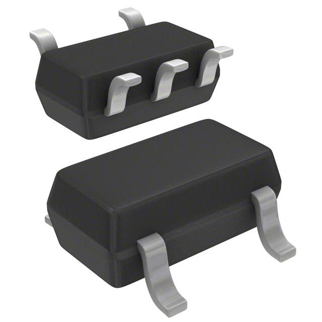
XR33180/81/83/84
3V to 5.5V, 52Mbps, TSOT23 RS-485/RS-422
Receivers with ±15kV ESD Protection
Description
The XR33180, XR33181, XR33183 and XR33184 are high performance
RS-485/RS-422 receivers designed to meet the increasing system
requirements found in today’s high performance serial communication
applications.
The receiver includes enhanced failsafe circuitry, guaranteeing
a logic-high receiver output when the receiver inputs are open,
shorted, or undriven. The XR33180/81/83/84 (XR3318x) receiver
input impedance is at least 48kΩ (1/4 unit load), allowing more than
128 devices on the bus. The bus pins are ESD protected and pass
IEC61000 level 4 (±15kV).
This is a wide supply (3.0V to 5.5V) device that operates at a maximum
data rate of 52Mbps and comes in very small 5-pin and 6-pin TSOT23
packages, making this standalone receiver ideal for high speed
point-to-point RS-485 applications where space is a concern.
The XR3318x offers several pinout options to maximize performance
in different applications while maintaining a minimum pin count. The
XR33180 is available in a 5-pin TSOT23 package with the receiver
always enabled. The XR33181 is available in a 6-pin TSOT23 package
and offers a active high receiver enable pin while the XR33183 has the
same pinout but with active low enable pin. The XR33184 is available
in a 6-pin TSOT23 package with a I/O logic supply pin to ease the
interface to MCU’s or FPGA’s that run off of different supply voltages.
The VL supply pin allows the XR33184 to interface to other devices
running off of supplies from ranging from 1.65V to VCC.
FEATURES
■■ Max 52Mbps data rate
■■ Wide 3.0V to 5.5V supply operation
■■ Robust Electrostatic Discharge (ESD)
protection for RS-485 bus pins
±15kV human body model
±15kV IEC61000-4-2 air discharge
±8kV IEC61000-4-2 contact
discharge
■■ Enhanced receiver failsafe protection for
open, shorted, or terminated but idle data
lines
■■ -40°C to 125°C ambient operating
temperature range
■■ Lead-free (RoHS 6) TSOT23-5 and
TSOT23-6 packaging
■■ Absolute minimum pin count option,
XR33180 (5-pin TSOT23)
■■ Tri-state RO options, XR33181 and
XR33183
■■ Adjustable I/O supply option to help
interfacing to lower voltage logic, XR33184
APPLICATIONS
■■ Clock distribution
■■ Robotic control
■■ Space constrained systems
■■ Security camera networks
■■ Industrial and process control equipment
All XR3318x options operate up to a max data rate of 52Mbps, and
have excellent propagation delay and skew characteristics making
them a good choice for clock fanout or clock distribution systems.
Typical Application
3.3V
3.3V to 5.0V
VCC
VCC
A
RO
120Ω
R
D
B
XR3319x
XR3318x
GND
GND
Figure 1. Typical Application
REV1C
1/12
�XR33180/81/83/84
Absolute Maximum Ratings
Operating Conditions
Stresses beyond those listed under Absolute Maximum
Ratings may cause permanent damage to the device.
Exposure to any Maximum Rating condition for extended
periods may affect device reliability and lifetime.
Operating temperature range....................... -40°C to 125°C
Supply voltage (VCC)....................................... -0.3V to 7.0V
Junction temperature.................................................. 150°C
Input Voltages
EN and EN....................................................... -0.3V to 7.0V
VCC supply range..............................................3.0V to 5.5V
Thermal Information
5-pin TSOT23 θJA............................................... 185.5°C/W
5-pin TSOT23 θJC................................................. 61.6°C/W
6-pin TSOT23 θJA............................................... 167.3°C/W
6-pin TSOT23 θJC................................................. 61.6°C/W
Output Voltage
RO (XR33180/81/83).......................... -0.3V to (VCC + 0.3V)
RO (XR33184)....................................... -0.3V to (VL + 0.3V)
Receiver Input Voltages
A, B............................................................................... ±18V
Transient voltage pulse, through 100Ω(1).................... ±100V
ESD Ratings
HBM - Human Body Model (A and B pins)................. ±15kV
HBM - Human Body Model (all other pins)................... ±4kV
IEC61000-4-2 Air Gap Discharge............................... ±15kV
IEC61000-4-2 Contact Discharge................................. ±8kV
NOTE:
1. Refer to Figure 3.
Electrical Characteristics
Specifications are at TA = 25°C, VCC = 3.0V to 5.5V unless otherwise noted. Typical values represent the most likely
parametric norm at TA = 25°C, and are provided for reference purposes only.
Symbol
Parameter
Conditions
Min
Typ
Max
Units
3.0
5.5
V
1.65
VCC
V
5
mA
10
μA
-50
mV
Supply
VCC
Supply voltage range
VL
I/O supply voltage range
VL ≤ VCC
ICC
Supply current
No Load, XR33180/81/83/84
IL
I/O supply
No Load, XR33184
2.5
Receiver DC Characteristics
VTH
Receiver differential threshold voltage,
VA - VB
-7V ≤ VCM ≤ 12V
∆VOH
Receiver input hysteresis
VCM = 0V
RIN
Receiver input resistance
-7V ≤ VCM ≤ 12V
IA,B
Input current, A and B
-200
-125
25
48
VOUT = 12V, VCC = 0V or 5.5V
VOUT = -7V, VCC = 0V or 5.5V
REV1C
mV
kΩ
250
-200
μA
μA
2/12
�XR33180/81/83/84
Electrical Characteristics
Specifications are at TA = 25°C, VCC = 3.0V to 5.5V unless otherwise noted. Typical values represent the most likely
parametric norm at TA = 25°C, and are provided for reference purposes only.
Symbol
Parameter
Conditions
Min
2
Typ
Max
Units
Logic Inputs/Outputs
VIH
Logic high input thresholds, EN and EN
XR33181/83
VIL
Logic low input thresholds, EN and EN
XR33181/83
IENLEAK
Enable pin leakage
XR33181/83
VOH
Receiver output high voltage, RO
IOUT = -4mA, XR33180/81/83
VOL
Receiver output low voltage, RO
IOUT = 4mA, XR33180/81/83
VOH
Receiver output high voltage, RO
3.0V ≤ VL ≤ 5.5V, IOUT = -4mA
1.65V ≤ VL ≤ 3.0V, IOUT = -1mA,
XR33184
VOL
Receiver output low voltage, RO
3.0V ≤ VL ≤ 5.5V, IOUT = 4mA
1.65V ≤ VL ≤ 3.0V, IOUT = 1mA,
XR33184
IOSC
Receiver output short-circuit current
0V ≤ VRO ≤ VL
IOZR
High-Z receiver output current
0V ≤ VOUT ≤ VCC, XR33180/81/83
0V ≤ VOUT ≤ VL, XR33184
V
-10
0.4
V
10
μA
VCC - 0.4
V
0.4
VL - 0.4
V
V
0.4
V
-120
120
mA
-1
1
μA
Thermal Characteristics
TTS
Thermal shutdown temperature
168
°C
TTSH
Thermal shutdown hysteresis
15
°C
Receiver AC Characteristics
tRPLH
Receiver propagation delay, low to high
tRPHL
Receiver propagation delay, high to low
|tRPLH - tRPHL|
Receiver propagation delay skew
CL = 15pF, VID = ±2V, VID rise and fall
times
