XR46000
N-Channel Power MOSFET
Description
The XR46000 is a silicon N-channel enhanced power MOSFET.
With low conduction loss, good switching performance and high
avalanche energy, it is suitable for various power supply system,
especially for AC step driving application for LED lighting.
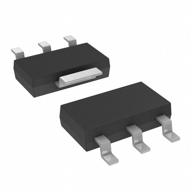
The package type is SOT-223, which comply with the RoHS standard.
APPLICATIONS
■■ LED lighting applications
Downlight
High bay
Specialty
Architectural
Key Parameters
VDSS
600V
ID
1.5A
PD (TC = 25°C)
20W
RDS,ON,typ
7.0Ω
FEATURES
■■ Fast switching
■■ ESD improved capability
■■ Low gate charge (Typ. 7.5nC)
■■ Low reverse transfer capacitance
(Typ. 5.0pF)
Equivalent Circuit
Pin Configuration
Drain
Drain
1
Gate
Gate
2
3
Drain Source
SOT-223, Top View
Source
Figure 1. Equivalent Cirucit
REV1B
1/6
�XR46000
Absolute Maximum Ratings
Operating Conditions
Stresses beyond the limits listed below may cause
permanent damage to the device. Exposure to any Absolute
Maximum Rating condition for extended periods may affect
device reliability and lifetime.
TJ operating junction temperature.............................. 150°C
TA operating ambient temperature................. -40°C to 85°C
TC = 25°C unless otherwise noted.
VDSS drain-to-source voltage....................................... 600V
ID continuous drain current (TC = 25°C)........................ 1.5A
ID continuous drain current (TC = 100°C).................... 0.85A
IDM pulsed drain current................................................... 6A
VGS gate-to-source voltage.......................................... ±30V
PD power dissipation (TC = 25°C)................................. 20W
PD derating factor above 25°C.............................. 0.16W/°C
TSTORAGE storage temperature range.......... -65°C to 150°C
EAS single pulse avalanche energy..............................80mJ
NOTE:
Unless otherwise noted, all tests are pulsed tests at the specified temperature,
therefore: TJ = TC = TA.
REV1B
2/6
�XR46000
Electrical Characteristics
TC = 25°C unless otherwise noted.
Symbol
Parameter
Conditions
Min
600
Typ
Max
Units
OFF Characteristic
BVDSS
Drain to source breakdown voltage
VGS = 0V, ID = 250µA
∆BVDSS/∆TJ
Breakdown voltage temperature coefficient
ID = 250µA, reference 25°C
IDSS
Drain to source leakage current
IGSS(F)
IGSS(R)
V
0.71
V/°C
VDS = 600V, VGS = 0V, TA = 25°C
25
VDS = 600V, VGS = 0V, TA = 125°C
250
Gate to source forward leakage
VGS = 30V
12
Gate to source reverse leakage
VGS = -28V
-12
µA
µA
ON Characteristic (pulse width tp ≤ 380µs, б ≤ 2%)
RDS(ON)
Drain to source on-resistance
VGS = 10V, ID = 0.75A
VGS(TH)
Gate threshold voltage
VDS = VGS, ID = 250µA
7.0
2.0
8.0
Ω
4.0
V
Dynamic Characteristic
gfs
Forward transconductance
Ciss
Input capacitance
Coss
Output capacitance
Crss
Reverse transfer capacitance
VDS = 15V, ID = 0.75A
1.0
s
170
VGS = 0V, VDS = 25V, f = 1MHz
27
pF
5
Resistive Switching Characteristic
td(ON)
Turn-on delay time
8
tr
Rise time
td(OFF)
Turn-off delay time
tf
Fall time
55
Qg
Total gate charge
7.5
Qgs
Gate to source charge
Qgd
Gate to drain “Miller” charge
ID = 1.5A, VDD = 300V, VGS = 10V,
RG = 4.7Ω
ID = 1.5A, VDD = 480V, VGS = 10V
30
ns
22
nC
1.7
4.0
Source-Drain Diode Characteristics (pulse width tp ≤ 380us, б ≤ 2%)
IS
Continuous source current (body diode)
1.5
ISM
Maximun source current (body diode)
6.0
VSD
Diode forward voltage
Trr
Reverse recovery time
Qrr
Reverse recovery charge
IRRM
Reverse recovery current
A
IS = 1.5A, VGS =0V
ID = 1.5A, TJ = 25°C, dIF/dt = 100A/µs,
VGS = 0V
REV1B
1.5
V
530
ns
1100
nC
4.4
A
3/6
�XR46000
Typical Performance Characteristics
ID, Drain Current (A)
10
10μs
1
10ms
100ms
0.1
Operation in this area may
be limited by RDS(ON)
0.01
TJ = 150°C
TC = 25°C
Single Pulse
0.001
DC
10
100
VDS, Drain-to-Source Voltage (V)
1
1000
Figure 2. Safe Operating Area
12
RDS(ON), Drain-to-Source
ON Resistance (Ω)
11
ID = 1.5A
10
Pulse duration = 10µs
Duty factor = 0.5% Max
TC = 25°C
ID = 0.75A
9
ID = 0.375A
8
7
6
6
4
8
10
VGS, Gate-to-Source Voltage (V)
12
14
Figure 3. Typical Drain-to-Source ON Resistance vs. Gate Voltage and Drain Current
RDS(ON), Drain-to-Source
ON Resistance, Normalized
2.5
2
VGS = 10V
ID = 250µA
1.5
1
0.5
0
-100
-50
0
100
50
TJ, Junction Temperature (°C)
150
200
Figure 4. Typical Drain-to-Source ON Resistance vs. Junction Temperature
REV1B
4/6
�XR46000
Package Description
REV1B
5/6
�XR46000
Ordering Information(1)
Part Number
XR46000ESETR
Operating
Temperature Range
Package
Packaging Method
Lead Free(2)
-40°C ≤ TJ ≤ 150°C
SOT-223
Tape and reel
Yes
NOTES:
1. Refer to www.maxlinear.com/XR46000 for most up-to-date Ordering Information.
2. Visit www.maxlinear.com for additional information on Environmental Rating.
Revision History
Revision
Date
Description
1A
Aug 2016
Initial release
1B
Nov 2019
Updated to MaxLinear logo. Updated Ordering Information.
5966 La Place Court
Suite 100
Carlsbad, CA 92008
Tel.: +1 (760) 692-0711
Fax: +1 (760) 444-8598
www.maxlinear.com
The content of this document is furnished for informational use only, is subject to change without notice, and should not be construed as a commitment by MaxLinear, Inc. MaxLinear, Inc. assumes
no responsibility or liability for any errors or inaccuracies that may appear in the informational content contained in this guide. Complying with all applicable copyright laws is the responsibility of the
user. Without limiting the rights under copyright, no part of this document may be reproduced into, stored in, or introduced into a retrieval system, or transmitted in any form or by any means (electronic,
mechanical, photocopying, recording, or otherwise), or for any purpose, without the express written permission of MaxLinear, Inc.
Maxlinear, Inc. does not recommend the use of any of its products in life support applications where the failure or malfunction of the product can reasonably be expected to cause failure of the life support
system or to significantly affect its safety or effectiveness. Products are not authorized for use in such applications unless MaxLinear, Inc. receives, in writing, assurances to its satisfaction that: (a) the
risk of injury or damage has been minimized; (b) the user assumes all such risks; (c) potential liability of MaxLinear, Inc. is adequately protected under the circumstances.
MaxLinear, Inc. may have patents, patent applications, trademarks, copyrights, or other intellectual property rights covering subject matter in this document. Except as expressly provided in any written
license agreement from MaxLinear, Inc., the furnishing of this document does not give you any license to these patents, trademarks, copyrights, or other intellectual property.
MaxLinear, the MaxLinear logo, and any MaxLinear trademarks, MxL, Full-Spectrum Capture, FSC, G.now, AirPHY and the MaxLinear logo are all on the products sold, are all trademarks of MaxLinear,
Inc. or one of MaxLinear’s subsidiaries in the U.S.A. and other countries. All rights reserved. Other company trademarks and product names appearing herein are the property of their respective owners.
© 2016 - 2019 MaxLinear, Inc. All rights reserved.
XR46000_DS_110119
REV1B
6/6
�