XR75100
40V Synchronous Step Down COT Controller
General Description
FEATURES
The XR75100 is a synchronous step-down controller for point-of load
supplies up to 20A. A wide 5.5V to 40V input voltage range allows for
single supply operation from industry standard 12V, 18V, and 24V DC and
AC rails.
With a proprietary emulated current mode Constant On-Time (COT)
control scheme, the XR75100 provides extremely fast line and load
transient response using ceramic output capacitors. It requires no loop
compensation hence simplifying circuit implementation and reducing
overall component count. The control loop also provides exceptional load
and line regulation and maintains constant operating frequency. A
selectable power saving mode allows the user to operate in discontinuous
mode (DCM) at light current loads, thereby significantly increasing the
converter efficiency.
A host of protection features, including over-current, over-temperature,
short-circuit and UVLO, help achieve safe operation under abnormal
operating conditions.
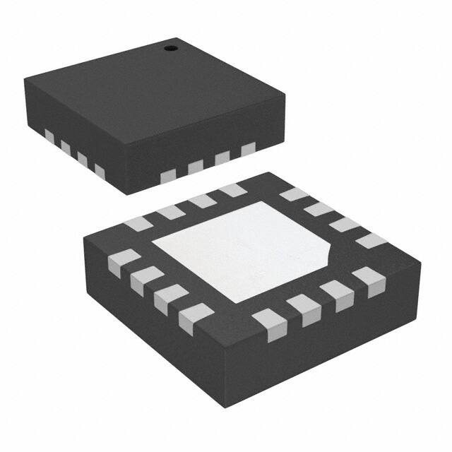
The XR75100 is available in a RoHS compliant, green / halogen free
space-saving 16-pin 3x3mm QFN package.
20A capable step-down controller
Wide 5.5V to 40V input voltage range
Integrated high current 2A / 3A drivers
0.6 to 30V adjustable output voltage
Proprietary Constant On-Time control
No loop compensation required
Stable ceramic output capacitor operation
Programmable 200ns to 2µs on-time
Constant 100kHz to 800kHz frequency
Selectable CCM or CCM / DCM operation
Programmable hiccup current limit with
thermal compensation
Precision enable and Power Good flag
Programmable soft-start
Integrated bootstrap diode
16-pin QFN package
APPLICATIONS
Networking and communications
Fast transient Point-of-Loads
Industrial and medical equipment
Embedded high power FPGA
Ordering Information – back page
Typical Application
3.340
VIN
CBST
VIN
EN/MODE
Q1
GH
3.320
VOUT
L1
Power Good
PGOOD
CIN
3.310
SW
RLIM
VCC
R3
CVCC
CSS
RON
XR75100 ILIM
SS
GL
TON
FB
AGND
Q2
CFF
R1
COUT
VOUT (V)
Enable/Mode
+0.5%
Typical
-0.5%
3.330
BST
3.300
3.290
3.280
R2
PGND
3.270
3.260
5
10
15
20
25
30
VIN (V)
1 / 16
maxlinear.com/XR75100
Rev 1E
�XR75100
Absolute Maximum Ratings
Operating Conditions
Stresses beyond the limits listed below may cause
permanent damage to the device. Exposure to any
Absolute Maximum Rating condition for extended periods
may affect device reliability and lifetime.
VIN.............................................................................-0.3V to 40V
VCC...........................................................................-0.3V to 5.5V
VIN.............................................................................-0.3V to 43V
PGOOD, TON, SS, EN, GL, FB................................-0.3V to 5.5V
VCC...........................................................................-0.3V to 6.0V
Switching frequency.......................................100kHz to 800kHz3
BST..........................................................................-0.3V to 48V2
Junction temperature range..............................-40°C to +125°C
SW, ILIM.....................................................................-1V to 40V1
BST-SW.......................................................................-0.3V to 6V
SW, ILIM..................................................................-5V to 43V1, 2
Note 1: SW pin’s minimum DC range is -1V, transient is -5V for less than
50ns.
GH...................................................................-0.3V to BST+0.3V
Note 2: No external voltage applied.
GH-SW........................................................................-0.3V to 6V
Note 3: Recommended
ALL other pins.................................................-0.3V to VCC+0.3V
Storage temperature...........................................-65°C to +150°C
Junction temperature..........................................................150°C
Power dissipation...............................................Internally Limited
Lead temperature (soldering, 10 sec).................................300°C
ESD rating (HBM - Human Body Model)................................2kV
Electrical Characteristics
Unless otherwise noted: TJ= 25°C, VIN = 24V, BST = VCC, SW = AGND = PGND = 0V, CGH = CGL = 3.3nF, 4.7µF at
VCC-AGND. Limits applying over the full operating temperature range are denoted by a “•”
Symbol
Parameter
Conditions
Min
Typ
Max
Units
40
V
2
mA
Power Supply Characteristics
VIN
Input voltage range
VCC regulating
IVIN
VIN input supply current
Not switching, VIN = 24V, VFB = 0.7V
IOFF
Shutdown current
5.5
0.7
f = 300kHz, RON = 215k, VFB = 0.58V
11
mA
Enable = 0V, VIN = 24V
0.1
µA
Enable and Under-Voltage Lock-Out UVLO
VIH_EN
EN pin rising threshold
VEN_HYS
EN pin hysteresis
VIH_EN
EN pin rising threshold for DCM/CCM
operation
VEN_HYS
EN pin hysteresis
1.8
1.9
2.0
50
2.9
3.0
mV
3.1
100
VCC UVLO start threshold, rising
edge
2 / 16
4.00
4.25
V
V
mV
4.50
V
maxlinear.com/XR75100
Rev 1E
�XR75100
Symbol
Parameter
Conditions
Min
VCC UVLO hysteresis
Typ
Max
200
Units
mV
Reference Voltage
VREF
Reference voltage
VIN = 5.5V to 40V
0.597
0.600
0.603
V
0.594
0.600
0.606
V
DC line regulation
CCM, closed loop, VIN = 5.5V-30V, applies
to any COUT
±0.3
%
DC load regulation
CCM, closed loop, IOUT = 0A-10A, applies
to any COUT
±0.15
%
2.0
µs
Programmable Constant On-Time
Maximum recommended on-time
RON = 237kΩ, VIN = 40V
On-time 1
RON = 237kΩ, VIN = 40V
f corresponding to on-time 1
VIN = 40V, VOUT = 24V
Minimum programmable on-time
RON = 14kΩ, VIN = 40V
120
RON = 14kΩ, VIN = 24V
200
230
ns
170
200
230
ns
1.7
2.0
2.3
µs
261
300
353
kHz
ns
On-time 2
RON = 14kΩ, VIN = 24V
f corresponding to on-time 2
VOUT = 5V
906
1042
1225
kHz
VOUT = 3.3V
598
688
809
kHz
430
506
582
ns
250
350
ns
-4
-1
2
mV
-14
-10
-6
µA
Fault present
1
VIN = 6V to 40V, ILOAD = 0 to 30mA
4.8
5.0
5.2
V
VIN = 5.5V, ILOAD = 0 to 20mA
4.8
5.0
5.2
V
-10
-7.5
-5
%
2
4
%
On-time 3
RON = 35.7kΩ, VIN = 24V
Minimum off-time
Diode Emulation Mode
Zero crossing threshold
DC value measured during test
Soft-start
SS charge current
SS discharge current
mA
VCC Linear Regulator
VCC output voltage
Power Good Output
Power Good threshold
Power Good hysteresis
Power Good sink current
1
mA
Protection: OCP, OTP, Short-Circuit
Hiccup timeout
110
ILIM pin source current
45
ILIM current temperature coefficient
50
0.4
3 / 16
ms
55
µA
%/°C
maxlinear.com/XR75100
Rev 1E
�XR75100
Symbol
Parameter
Conditions
OCP comparator offset
Min
Typ
Max
Units
-8
0
+8
mV
Current limit blanking
GL rising>1V
100
ns
Thermal shutdown threshold1
Rising temperature
150
°C
15
°C
Thermal hysteresis1
VSCTH feedback pin short-circuit
threshold
Percent of VREF, short circuit is active
after PGOOD is up
50
60
70
%
Output Gate Drivers
GH pull-down resistance
IGH = 200mA
1.35
2.0
Ω
GH pull-up resistance
IGH = 200mA
1.8
2.8
Ω
GL pull-down resistance
IGL = 200mA
1.35
1.9
Ω
GL pull-up resistance
IGL = 200mA
1.7
2.7
Ω
GH and GL pull-down resistance
50
kΩ
GH and GL rise time
10% to 90%
35
50
ns
GH and GL fall time
90% to 10%
30
40
ns
GL to GH non-overlap time
Measured GL falling edge = 1V to GH
rising edge = 1V, BST = VCC, SW = 0V
30
60
ns
GH to GL non-overlap time
Measured GH falling edge = 1V to GL
rising edge = 1V
20
40
ns
Note 1: Guaranteed by design.
4 / 16
maxlinear.com/XR75100
Rev 1E
�XR75100
Pin Configuration
PGND
VCC
VIN
AGND
16
15
14
13
GL
1
12 AGND
NC
2
11 FB
EXPOSED PAD
SW
3
GH
4
10 PGOOD
9
5
6
7
8
BST
ILIM
EN
TON
SS
Pin Assignments
Pin No.
Pin Name
Type
1
GL
2
NC
3
SW
A
Lower supply rail for high-side gate driver GH. Connect this pin to the junction between the two
external N-channel MOSFETs.
4
GH
O
Driver output for high-side N-channel switching MOSFET.
5
BST
A
High-side driver supply pin. Connect a 0.1µF bootstrap capacitor between BST and SW.
6
ILIM
A
Over-current protection programming. Connect with a resistor to the drain of the low-side
MOSFET.
7
EN/MODE
I
Precision enable pin. Pulling this pin above 1.9V will turn the IC on and it will operate in Forced
CCM. If the voltage is raised above 3.0V, then the IC will operate in DCM or CCM depending
on load.
8
TON
A
Constant on-time programming pin. Connect with a resistor to AGND.
9
SS
A
Soft-start pin. Connect an external capacitor between SS and AGND to program the soft-start
rate based on the 10µA internal source current.
10
PGOOD
OD
Power-good output. This open-drain output is pulled low when VOUT is outside the regulation.
11
FB
A
Feedback input to feedback comparator. Connect with a set of resistors to VOUT and GND in
order to program VOUT.
AGND
A
Analog ground. Control circuitry of the IC is referenced to this pin.
12, 13
O
Description
Driver output for low-side N-channel synchronous MOSFET.
Internally not connected. Leave this pin floating.
14
VIN
PWR
IC supply input. Provides power to internal LDO.
15
VCC
PWR
The output of LDO. For operation using a 5V rail, VCC should be shorted to VIN.
16
PGND
PWR
Low side driver ground.
Exposed Pad
A
Thermal pad for heat dissipation. Connect to AGND with a short trace.
Type: A = Analog, I = Input, O = Output, I/O = Input/Output, PWR = Power, OD = Open-Drain
5 / 16
maxlinear.com/XR75100
Rev 1E
�XR75100
Functional Block Diagram
VCC
TON
VCC UVLO
Enable LDO
4.25 V
VIN
Switching
Enabled
+
-
LDO
VCC
VCC
OTP
TJ
150 C
PGOOD
10uA
SS
+
+
FB
0.6V
-
Current
emulation &
DC correction
VIN
On-Time
-
BST
Switching
Enabled
0.6 V
Feedback
comparator
TON
+
FB
-
R
Q
S
Q
PGOOD comparator
+
+
-
R
Q
S
Q
GL
Enable
Hiccup
Hiccup
Mode
Enable LDO
+
1.9 V
Enable LDO
-
If four
consecutive OCP
Forced CCM or DCM/CCM
+
3V
-
If 8 consecutive ZCD
Then DCM
If 1 non-ZCD
Then exit DCM
50uA
+
-
EN/Mode
SW
VCC
Switching
Enabled
Short-circuit detection
0.36 V
Dead
Time
Control
Minimum
On Time
-
0.555 V
GH
OCP
comparator
Zero Cross Detect
SW
+
-1 mV
-
AGND
6 / 16
ILIM
PGND
maxlinear.com/XR75100
Rev 1E
�XR75100
Typical Performance Characteristics
Unless otherwise noted: VIN = 24V, VOUT = 3.3V, IOUT = 10A, f = 500kHz, TA = 25°C. Schematic from the application
information section.
3.340
3.330
+0.5%
Typical
-0.5%
3.330
3.320
3.320
3.310
3.310
VOUT (V)
VOUT (V)
3.340
+0.5%
Typical
-0.5%
3.300
3.290
3.300
3.290
3.280
3.280
3.270
3.270
3.260
3.260
0
2
4
6
8
10
5
IOUT (A)
10
15
20
25
30
VIN (V)
Figure 1: Load Regulation
Figure 2: Line Regulation
Figure 3: Load Step, Forced CCM, 0A - 6.5A - 0A
Figure 4: Load Step, DCM / CCM, 0A - 6.5A - 0A
Figure 5: Steady State, VOUT,ripple = 14mV, IOUT = 10A
Figure 6: Steady State, DCM, VOUT,ripple = 61mV, IOUT = 0A
7 / 16
maxlinear.com/XR75100
Rev 1E
�XR75100
1,400
1,000
Typical
Typical
1,200
Calculated
Calculated
TON (ns)
TON (ns)
1,000
100
800
600
400
200
10
0
1
10
100
5
10
RON (kΩ)
20
25
30
VIN (V)
Figure 8: TON versus VIN, RON = 19.1kΩ
Figure 7: TON versus RON, VIN = 24V
600
600
550
550
500
500
f (kHz)
f (kHz)
15
450
450
400
400
350
350
300
300
0
2
4
6
8
10
5
10
IOUT (A)
15
20
25
30
VIN (V)
Figure 9: Frequency versus IOUT, VIN = 24V
Figure 10: Frequency versus VIN, IOUT = 10A
610
16
14
605
10
VREF (mV)
IOCP (A)
12
8
6
4
600
595
2
0
590
0.5
0.6
0.7
0.8
0.9
1
-40 -20 0
20 40 60 80 100 120
TJ (°C)
RLIM (kΩ)
Figure 12: VREF versus Temperature
Figure 11: IOCP versus RLIM
8 / 16
maxlinear.com/XR75100
Rev 1E
�XR75100
550
70
530
510
ILIM (uA)
TON (ns)
60
490
50
40
470
30
450
-40 -20 0
-40 -20 0
20 40 60 80 100 120
TJ (°C)
TJ (°C)
Figure 13: TON versus Temperature
Figure 14: ILIM versus Temperature
Figure 15: Power-up, Forced CCM
Figure 16: Power-up, DCM / CCM
100
Efficiency (%)
20 40 60 80 100 120
5.0V_CCM
5.0V_DCM
95
3.3V_CCM
3.3V_DCM
90
2.5V_CCM
2.5V_DCM
85
80
75
70
65
60
55
50
0.1
1
10
IOUT (A)
Figure 17: Efficiency, VIN = 24V, f = 500kHz
9 / 16
maxlinear.com/XR75100
Rev 1E
�XR75100
Functional Description
XR75100 is a synchronous step-down, proprietary
emulated current-mode Constant On-Time (COT)
controller. The on-time, which is programmed via
RON, is inversely proportional to VIN and maintains
a nearly constant frequency. The emulated current-mode
control is stable with ceramic output capacitors.
an external control is not available, the EN/MODE input can
be derived from VIN. If VIN is well regulated, use a resistor
divider and set the voltage to 4V. If VIN varies over a wide
range, the circuit shown in Figure 19 can be used
to generate the required voltage.
V
IN
RZ
10k
Each switching cycle begins with GH signal turning on the
high-side (control) FET for a preprogrammed time. At the
end of the on-time, the high-side FET is turned off and the
low - side (synchronous) FET is turned on for a preset
minimum time (250ns nominal). This parameter is termed
Minimum Off-Time. After the Minimum Off-Time, the voltage
at the feedback pin FB is compared to an internal voltage
ramp at the feedback comparator. When VFB drops below
the ramp voltage, the high-side FET is turned on and the
cycle repeats. This voltage ramp constitutes an emulated
current ramp and makes the use of ceramic capacitors
possible, in addition to other capacitor types, for output
filtering.
R1
30.1k, 1%
Z ener
M M SZ4685T1G or Equivalent
EN /M OD E
R2
35.7k, 1%
Figure 18: Selecting Forced CCM
by Deriving EN/MODE from VIN
Enable/Mode Input (EN/MODE)
EN/MODE pin accepts a tri-level signal that is used to
control turn on and off. It also selects between two modes
of operation: ‘Forced CCM’ and ‘DCM / CCM’. If EN is
pulled below 1.8V, the controller shuts down. A voltage
between 2.0V and 2.9V selects the Forced CCM mode,
which will run the converter in continuous conduction at
all times. A voltage higher than 3.1V selects the DCM /
CCM mode, which will run the converter in discontinuous
conduction at light loads.
V
IN
RZ
10k
V
EN/MODE
EN
Zener
MMSZ4685T1G or Equivalent
Selecting the Forced CCM Mode
In order to set the controller to operate in Forced CCM, a
voltage between 2.0V and 2.9V must be applied to
EN/MODE. This can be achieved with an external control
signal that meets the above voltage requirement.
Where an external control is not available, the EN/MODE
can be derived from VIN. If VIN is well regulated, use a
resistor divider and set the voltage to 2.5V. If VIN varies over
a wide range, the circuit shown in Figure 18 can be
used to generate the required voltage. Note that at VIN of
5.5V and 40V, the nominal Zener voltage is 4.0V
and 5.0V respectively. Therefore for VIN in the range of
5.5V to 40V, the circuit shown in Figure 18 will generate VEN
required for Forced CCM.
Selecting the DCM/CCM Mode
In order to set the controller operation to DCM / CCM, a
voltage between 3.1V and 5.5V must be applied to
EN/MODE. If an external control signal is available, it can
be directly connected to EN/MODE. In applications where
Figure 19: Selecting DCM / CCM
by Deriving EN/MODE from VIN
DCM Operation
When DCM operation is enabled, the Zero Cross Detect
comparator in the XR75100 senses when the current in the
inductor reaches 0Amps and turns off the low side
MOSFET. The low side MOSFET is operated to emulate
the operation of a diode preventing the inductor current
from flowing in the negative direction. In this mode, the
device is now operating in Pulse Frequency Modulation
(PFM) control. As the load reduces, the frequency reduces
and thus the switching losses are reduced, resulting in
10 / 16
maxlinear.com/XR75100
Rev 1E
�XR75100
much better efficiency at light load. The Zero Cross
comparator monitors the voltage across the low side
MOSFET to determine the correct time to turn it off.
Ideally, this threshold is -1mV, meaning there is still positive current in the inductor (positive inductor current refers
to current from SW to VOUT). However, there is a range to
the sensed voltage from -4mV to +2mV. In the case where
a very low RDSON low side MOSFET is used, a higher
negative inductor current is required to reach the +2mV. For
instance, a 2mΩ MOSFET would require a negative 1A
inductor valley current before the XR75100 recognizes the
signal to turn off the low side MOSFET. As a result, the
XR75100 will not enter PFM until the load reduces further. It
should be noted that the net power saving between ideal
zero cross detection and the -4mV to +2mV range of the
XR75100 is minor. The operating frequency will have
changed little from what one would have in the ideal case.
One important feature added to the DCM detection is a
counter which allows 8 switching cycles to trigger in the
zero cross comparator before enabling DCM operation.
This ensures that during large unloading events, the
XR75100 will respond quickly. This operation can be seen
during the unloading event in Figure 4 in the Typical
Performance Characteristics section above.
Programming the On-Time
The On-Time TON is programmed via resistor RON
according to following equation:
hiccup timeout will repeat. The IC will remain in hiccup
mode until load current is reduced below the programmed IOCP. In order to program over-current protection, use the following equation:
I OCP RDS + 8mV
RLIM = -----------------------------------------------------ILIM
Where:
RLIM is resistor value for programming IOCP
IOCP is the over-current threshold to be programmed
RDS is the MOSFET rated on resistance
8mV is the OCP comparator offset
ILIM is the internal current that generates the necessary
OCP comparator threshold (use 45μA).
Note that ILIM has a positive temperature coefficient of
0.4%/°C. This is meant to roughly match and compensate
for the positive temperature coefficient of the synchronous
FET RDS. In order for this feature to be effective, the
temperature rise of the IC should approximately match the
temperature rise of the FET. A graph of typical IOCP versus
RLIM is shown in Figure 11.
Short-Circuit Protection (SCP)
If the output voltage drops below 60% of its programmed
value, the IC will enter hiccup mode. Hiccup will persist until
the short-circuit is removed. The SCP circuit becomes
active after PGOOD asserts high.
V IN TON
RON = ---------------------------– 10
3.4 10
Over-Temperature (OTP)
where TON is calculated from:
OTP triggers at a nominal die temperature of 150°C. The
gate of the switching FET and synchronous FET are turned
off. When die temperature cools down to 135°C, soft-start
is initiated and operation resumes.
V OUT
TON = ---------------V IN f
Programming the Output Voltage
As an example, the calculated TON for the application
circuit is 275ns. An RON of 19.4kΩ is required in order to
set TON to 275ns. A graph of typical TON versus RON is
shown in Figure 7.
Use an external voltage divider as shown in the application
circuit to program the output voltage VOUT.
V OUT
R1 = R2 ------------- – 1
0.6
Over-Current Protection (OCP)
If load current exceeds the programmed over-current IOCP
for four consecutive switching cycles, then the IC enters hiccup mode of operation. In hiccup mode, the MOSFET gates
are turned off for 110ms (hiccup timeout). Following the hiccup timeout, a soft-start is attempted. If OCP persists,
where R2 has a nominal value of 2kΩ.
11 / 16
maxlinear.com/XR75100
Rev 1E
�XR75100
Programming the Soft-start
Place a capacitor CSS between the SS and GND pins to
program the soft-start. In order to program a soft-start time
of TSS, calculate the required capacitance CSS from the
following equation:
2. The frequency of ESR Zero fZero,ESR should be at least
five times larger than fLC.
Feed-Forward Capacitor (CFF)
A feed - forward capacitor (CFF) may be necessary,
depending on the Equivalent Series Resistance (ESR) of
COUT. If only ceramic output capacitors are used for COUT,
then a CFF is necessary. Calculate CFF from:
C FF
where:
R1 is the resistor that CFF is placed in parallel with
fLC is the frequency of output filter double-pole
When using capacitors with higher ESR, such as
PANASONIC TPE series, a CFF is not required provided
following conditions are met:
1. The frequency of output filter LC double-pole fLC should
be less than 10kHz.
10A
CSS = TSS --------------
0.6V
1
= ------------------------------------------------2 R 1 7 f LC
fLC must be less than 11kHz when using a ceramic COUT. If
necessary, increase COUT and / or L in order to meet this
constraint.
Note that if fZero,ESR is less than 5xfLC, then it is
recommended to set the fLC at less than 2kHz. CFF is still
not required.
Feed-Forward Resistor (RFF)
Poor PCB layout and / or extremely fast switching FETs can
cause switching noise at the output and may couple to the
FB pin via CFF. Excessive noise at FB will cause poor load
regulation. To solve this problem, place a resistor RFF in
series with CFF. An RFF value up to 2% of R1 is acceptable.
Maximum Allowable Voltage Ripple at FB pin
Note that the steady-state voltage ripple at feedback pin FB
(VFB,RIPPLE) must not exceed 50mV in order for the Module
to function correctly. If VFB,RIPPLE is larger than 50mV, then
COUT should be increased as necessary in order to keep
the VFB,RIPPLE below 50mV.
12 / 16
maxlinear.com/XR75100
Rev 1E
�XR75100
Application Circuit
2k
18.2k
VIN
24VIN
VIN
EN/MODE
2 x 10uF
RLIM 1k
19.1k
5
BST
ILIM
7
XR75100
FB
NC
CIN
CVCC
0.1uF
4.7uF
L1 IHLP-5050FD-01
1.5uH, 27A
4
3
500kHz, 3.3V @ 0-10A
VOUT
2
CFF
0.22nF
PGND
1
MB, SiR642DP
3mOhm
16
EXPAD
GL
VCC
AGND
VIN
17
SW
U1
15
12
PGOOD
13
VFB
11
GH
14
10
10k
SS
AGND
9
VCC
EN
PWRGD
MT, SiR426DP
12.5mOhm
CBST 1uF
6
8
RON
TON
CSS
47nF
RFF
40 Ohm
3 x 47uF
R1
9.09k
VFB
VIN
VCC
R2
2k
13 / 16
maxlinear.com/XR75100
Rev 1E
�XR75100
Mechanical Dimensions
16-Pin QFN
16X L
TOP VIEW
16X b
BOTTOM VIEW
SIDE VIEW
TERMINAL DETAILS
Drawing No.: POD- 00000138
Revision: A
14 / 16
maxlinear.com/XR75100
Rev 1E
�XR75100
Recommended Land Pattern and Stencil
TYPICAL RECOMMENDED LAND PATTERN
TYPICAL RECOMMENDED STENCIL
Drawing No.: POD- 00000138
Revision: A
15 / 16
maxlinear.com/XR75100
Rev 1E
�XR75100
Ordering Information(1)
Part Number
Operating Temperature Range
Package
Packaging Method
Lead-Free(2)
XR75100EL-F
-40°C ≤ TJ ≤ +125°C
16-pin QFN 3 x 3
Bulk
Yes
XR75100ELTR-F
-40°C ≤ TJ ≤ +125°C
16-pin QFN 3 x 3
Reel
Yes
XR75100EVB
Evaluation Board
NOTES:
1. Refer to www.maxlinear.com/XR75100 for most up-to-date Ordering Information
2. Visit www.maxlinear.com for additional information on Environmental Rating.
Revision History
Revision
Date
Description
1A
June 2014
Initial release
1B
March 2015
1C
May 2016
Add limits to zero cross and clarify operating temperature range.
1D
May 2018
Update to MaxLinear logo. Update format and Ordering Information. Added Revision History.
1E
October 2019
Correct block diagram by changing the input gate into the Hiccup Mode from an AND gate to
an OR gate. Update ordering information.
Modified Functional Block Diagram, Application Circuit, figure 18 and 19. Changed the description of “Selecting the Forced CCM Mode”, “Selecting the DCM/CCM Mode”, “Feed-Forward
Capacitor”, Feed-Forward Resistor”, Added “Maximum Allowable Voltage Ripple at FB PIN”.
Corporate Headquarters:
5966 La Place Court
Suite 100
Carlsbad, CA 92008
Tel.:+1 (760) 692-0711
Fax: +1 (760) 444-8598
www.maxlinear.com
The content of this document is furnished for informational use only, is subject to change without notice, and should not be construed as a commitment by MaxLinear, Inc. MaxLinear, Inc. assumes no
responsibility or liability for any errors or inaccuracies that may appear in the informational content contained in this guide. Complying with all applicable copyright laws is the responsibility of the user. Without
limiting the rights under copyright, no part of this document may be reproduced into, stored in, or introduced into a retrieval system, or transmitted in any form or by any means (electronic, mechanical, photocopying, recording, or otherwise), or for any purpose, without the express written permission of MaxLinear, Inc.
Maxlinear, Inc. does not recommend the use of any of its products in life support applications where the failure or malfunction of the product can reasonably be expected to cause failure of the life support
system or to significantly affect its safety or effectiveness. Products are not authorized for use in such applications unless MaxLinear, Inc. receives, in writing, assurances to its satisfaction that: (a) the risk of
injury or damage has been minimized; (b) the user assumes all such risks; (c) potential liability of MaxLinear, Inc. is adequately protected under the circumstances.
MaxLinear, Inc. may have patents, patent applications, trademarks, copyrights, or other intellectual property rights covering subject matter in this document. Except as expressly provided in any written
license agreement from MaxLinear, Inc., the furnishing of this document does not give you any license to these patents, trademarks, copyrights, or other intellectual property.
MaxLinear, the MaxLinear logo, and any MaxLinear trademarks, MxL, Full-Spectrum Capture, FSC, G.now, AirPHY and the MaxLinear logo are all on the products sold, are all trademarks of MaxLinear, Inc.
or one of MaxLinear’s subsidiaries in the U.S.A. and other countries. All rights reserved. Other company trademarks and product names appearing herein are the property of their respective owners.
© 2016 - 2019 MaxLinear, Inc. All rights reserved
16 / 16
maxlinear.com/XR75100
Rev 1E
�