XRP1117
800mA Low Dropout Positive Voltage Regulator
May 2013
Rev. 1.0.0
GENERAL DESCRIPTION
APPLICATIONS
The XRP1117 is a low power positive-voltage
low dropout regulator capable of providing up
to 800mA of output load current. This device is
available in a fixed 3.3V output voltage and an
adjustable output voltage version.
The XRP1117 is optimized for low voltage
operations where transient response and
minimum input voltage are critical. Dropout
voltage is guaranteed at a maximum of 1.3V
at 800mA, decreasing at lower load currents.
As the load current decreases, the quiescent
current flows into the load effectively
increasing the efficiency of the regulator. On
chip trimming adjusts the reference/output
voltage to within ± 1%.
Built-in over temperature and over-current
protection insures safe operation under
abnormal operating conditions.
The XRP1117 is available in a RoHS compliant,
green/halogen free space-saving and low
profile 3-pin SOT223 package.
• Desktop PC Server
• Graphic/Video Card
• Industrial Equipment
• Power Supplies Post Regulation
FEATURES
• Guaranteed 800mA Output Current
− 1A Peak Current
− 1.35A Typical Current Limit
• Adjustable and 3.3V Fixed Output
Voltage Options
− ±1% Accuracy
• 1.2V Low Dropout Voltage
• Low Quiescent Current
• Over Current and Thermal Protection
• Lead Free, RoHS Compliant SOT223
Package
FUNCTIONAL DIAGRAM
Fig. 1: XRP1117 Application Diagram
Exar Corporation
48720 Kato Road, Fremont CA 94538, USA
www.exar.com
Tel. +1 510 668-7000 – Fax. +1 510 668-7001
�XRP1117
800mA Low Dropout Positive Voltage Regulator
ABSOLUTE MAXIMUM RATINGS
OPERATING RATINGS
These are stress ratings only and functional operation of
the device at these ratings or any other above those
indicated in the operation sections of the specifications
below is not implied. Exposure to absolute maximum
rating conditions for extended periods of time may affect
reliability.
Input Voltage VIN .................................................... 15V
Operating Junction Temperature ...............-40°C to 125°C
Maximum Output Current.............................. 800mA min
Thermal Resistance .....................................................
θJC....................................................................................................... 15°C/W
θJA (see Thermal Characteristics in the Application
Information)
Input Supply Voltage VIN ......................................... 18V
Junction Temperature .......................................... 150°C
Lead Temperature (Soldering, 10 sec) ................... 260°C
Storage Temperature .............................. -65°C to 150°C
ESD Rating (HBM - Human Body Model) .................... 2kV
ELECTRICAL SPECIFICATIONS
Specifications are for an Operating Ambient Temperature of TA = TJ = 25°C only; limits applying over the full Operating
Junction Temperature range are denoted by a “•”. Minimum and Maximum limits are guaranteed through test, design, or
statistical correlation. Typical values represent the most likely parametric norm at TJ = 25°C, and are provided for reference
purposes only. Unless otherwise indicated, VIN = VOUT + 2V, IOUT = 10mA, TA = TJ = 25°C.
Parameter
Min.
Typ.
Max.
3.267
3.235
3.300
3.333
3.365
6
10
15
Units
Conditions
3.3V Version
Output Voltage
0.5
Line Regulation
Load Regulation
2
V
mV
•
•
1.5V≤(VIN–VOUT)≤10V
1.5V≤(VIN–VOUT)≤10V
mV
Adjustable Voltage Version
Load Regulation
0.4
1.262
1.270
0.1
0.2
1
Adjust Pin Current
60
120
µA
•
Adjust Pin Current Change
0.2
5
µA
•
1.5V≤(VIN–VOUT)≤10V
Minimum Load Current
1.7
5
mA
•
1.5V≤(VIN–VOUT)≤10V
1.2
1.3
V
Reference Voltage
1.238
1.225
1.250
0.001
Line Regulation
V
%
•
•
1.5V≤(VIN–VOUT)≤10V
1.5V≤(VIN–VOUT)≤10V
%
All Voltage Options
Dropout Voltage
Current Limit
1.35
A
Ripple Rejection
70
dB
Output Voltage Temperature
Stability
0.5
%
1.0
IOUT=800mA, ∆VREF=1%2
f=120Hz, COUT=22µF, IOUT=300mA,
(VIN–VOUT)=3V
RMS Output Noise
0.003
%
% of VOUT, 10Hz≤f≤10kHz
Thermal Shutdown
160
°C
Junction temperature
16
°C
Thermal Shutdown Hysteresis
Note 2: Dropout voltage is the input voltage minus output voltage that produces a 1% decrease in output voltage with
respect to the nominal output voltage at VIN=VOUT+2V
© 2013 Exar Corporation
2/9
Rev. 1.0.0
�XRP1117
800mA Low Dropout Positive Voltage Regulator
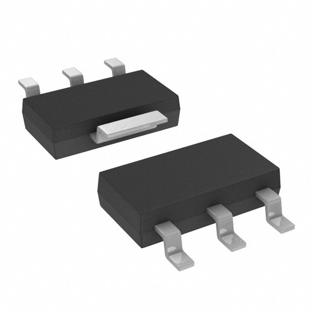
PIN ASSIGNMENT
Fig. 2: XRP1117 Pin Assignment (Top View, TAB connected to VOUT)
ORDERING INFORMATION
Part Number
Temperature
Range
XRP1117ESETR-F
-40°C≤TJ≤+125°C
XRP1117ESETR-33-F
-40°C≤TJ≤+125°C
Marking
1117ESE
YYWWF
1117ESE
33YYWWF
Package
Packing
Quantity
Note 1
SOT223-3
2.5K/Tape & Reel Halogen Free
SOT223-3
2.5K/Tape & Reel Halogen Free
Note 2
Adjustable
Output Voltage
3.3V Output
Voltage
“YY” = Year – “WW” = Work Week – “F” = Halogen Free Indicator - “X” = Lot Number
© 2013 Exar Corporation
3/9
Rev. 1.0.0
�XRP1117
800mA Low Dropout Positive Voltage Regulator
TYPICAL PERFORMANCE CHARACTERISTICS
All data taken at TA = TJ = 25°C, unless otherwise specified - Schematic and BOM from Application Information section of
this datasheet.
Fig. 3: Reference Voltage vs Juction Temperature
XRP1117ESETR-F, VIN=4.5V, IOUT=10mA
Fig. 4: Minimum Load Current vs Junction Temperature
XRP1117ESETR-F, VIN=4.5V
Fig. 5: Dropout Voltage vs. Output Current
Fig. 6: Line Transient Response
Fig. 7: Load Transient Response, 10mA-800mA
Fig. 8: PSRR vs. Frequency
© 2013 Exar Corporation
4/9
Rev. 1.0.0
�XRP1117
800mA Low Dropout Positive Voltage Regulator
Fig. 9: Current Limit vs. Junction Temperature
VIN=4.5V, no heatsink, VOUT= VOUT(nom)x98%
Fig. 10: Dropout Voltage vs. Junction Temperature
APPLICATION INFORMATION
5.0mA minimum
regulation.
OUTPUT VOLTAGE
For fixed voltage option, the resistors R1 and
R2 are included in the regulator.
The typical application circuits for the
adjustable output regulator are shown below
in Figures 15.
is
required
for
INPUT CAPACITOR
A XRP1117 device located more than a few
inches away from the power source may
require an input bypass capacitor Cin for
regulator stability. This capacitor will reduce
the circuit’s sensitivity when powered from a
complex source impedance and significantly
enhance the output transient response. The
input bypass capacitor should be mounted
with the shortest possible traces as close as
possible to the regulator’s input and ground
terminals. A 10µF ceramic or tantalum
capacitor should be adequate for most
applications.
The adjustable output voltage device is a
floating voltage regulator. The XRP1117
develops and maintains a nominal 1.25 V
reference voltage between the output and
adjust pins. The reference voltage is
programmed to a constant current source by
resistor R1, and this current flows through R2
to ground to set the output voltage.
The output of the adjustable regulator can be
set to any voltage between 1.25V and 15V.
The value of VOUT can be quickly approximated
using the formula
1.25
OUTPUT CAPACITOR
The XRP1117 requires an output capacitor of
at least 22µF (tantalum or ceramic or
Aluminum Electrolytic) to ensure stability. The
value may change based on the application
requirements
of
the
output
load
or
temperature range. The value of ESR can vary
based on the type of capacitor used in the
applications to guarantee stability. The
recommended value for ESR is 0.5Ω or less. A
larger value of output capacitance (up to
100µF) can improve the loop stability and load
A small correction to this formula is required
depending on the values of resistors R1 and
R2, since the adjustable pin current (approx
50µA) flows through R2. When IADJ is taken
into account, the formula becomes
Where VREF=1.25V
The programmed current level is usually
selected to be greater than the specified
© 2013 Exar Corporation
that
5/9
Rev. 1.0.0
�XRP1117
800mA Low Dropout Positive Voltage Regulator
transient response as well as reducing output
noise.
and input pins of the device can withstand
microsecond surge currents. A combination of
large output capacitors and an input pin
instantaneously shorted to ground may cause
some damage to the device; under these
conditions, a diode between the output
(anode)
and
input
(cathode)
pins
is
recommended.
SOLDERING METHODS
The XRP1117 SOT-223 package is designed to
be compatible with infrared reflow or vaporphase reflow soldering techniques. During
soldering, the non-active or mildly active
fluxes may be used. The XRP1117 die is
attached to the heatsink lead which exits
opposite the input, output, and ground pins.
Fig. 11: Load Step Response 10mA to 800mA
VIN=3.3V, VOUT=1.8V, CIN=10µF, COUT=22µF Ceramic
ch1=VOUT, ch4=ILOAD, time=100us/div
Hand soldering and wave soldering should be
avoided since these methods can cause
damage to the device with excessive thermal
gradients on the package. The SOT-223
recommended soldering method are as
follows: vapor phase reflow and infrared
reflow with the component preheated to within
65°C of the soldering temperature range.
THERMAL CHARACTERISTICS
The junction-to-ambient thermal resistance
(θJA) of XRP1117 is dependent on the PCB
layout. The XRP1117 features an internal
thermal limiting circuitry to protect the device
during overload conditions. Special care needs
to be taken during continuous load conditions
such that the maximum junction temperature
does not exceed 125 °C. Thermal protection is
activated at >160°C and deactivated at
很抱歉,暂时无法提供与“XRP1117ESETR-33-F”相匹配的价格&库存,您可以联系我们找货
免费人工找货