X RP 6 8 4 0
4.3A Supercapacitor Flash LED Driver with I2C
December 2009
Rev. 1.0.0
GENERAL DESCRIPTION
APPLICATIONS
The XRP6840 is a controlled-current dual-cell
supercapacitor charger and high power LED
driver. Operating from a standard lithium-ion
battery, the XRP6840 provides up to 4.3A of
programmable Flash LED current and up to
600mA
and
5.6V
of
programmable
supercapacitor charging current and voltage.
Architectured around a 2.4MHz tri-mode 1x,
1.5x and 2x charge pump, the XRP6840
charges the stacked supercapacitor to the
programmed output voltage with no more
than 600mA drawn from the battery. While
charging, an internal active balance circuitry
insures matching of the stacked capacitors’
voltages.
A standard 2-line I2C serial interface allows
the dynamic programming of LED currents in
torch and flash modes, flash timeout, channel
enable, gain control, capacitor charge voltage,
and enable. The XRP6840 comes in a 2 and 3
channel
version
supporting
respectively
440mA/2.15A per channel and 300mA/1.45A
in torch/flash modes.
The flexibility designed into the XRP6840 can
also allow it to reverse the power flow back to
the input to prevent unintended system resets
as the battery voltage drops.
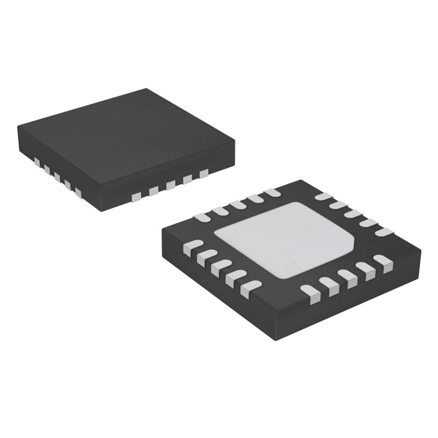
The XRP6840 is available in a lead-free,
“green”/halogen free 20-pin TQFN package.
• High Power Torch/Strobe/Flash LED
• High Resolution Cameras
• Generic High Power Lighting
• High Power White LED Backlighting
FEATURES
• Programmable 4.3A Flash LED Driver
− Torch and Flash Modes
− 2 and 3 Channels Versions
• Programmable Supercapacitor Charger
− 600mA Adjustable Charging Current
− Programmable Supercapacitor Voltage
− In-rush Current Control
− Active Voltage Balance Control
• Tri-mode Charge Pump Architecture
− 1x, 1.5x, 2x Operation Modes
− 2.4MHz Switching Frequency
• I2C Serial Interface
• Thermal, Over Current and Output
Short Protection
• LED Short Detection
• RoHS Compliant “Green”/Halogen Free
20-pin 4mmx4mm TQFN package
TYPICAL APPLICATION DIAGRAM
Fig. 1: XRP6840 – 3 Channels Application Diagram
Exar Corporation
48720 Kato Road, Fremont CA 94538, USA
www.exar.com
Tel. +1 510 668-7000 – Fax. +1 510 668-7001
�X RP 6 8 4 0
4.3A Supercapacitor Flash LED Driver with I2C
ABSOLUTE MAXIMUM RATINGS
OPERATING RATINGS
These are stress ratings only and functional operation of
the device at these ratings or any other above those
indicated in the operation sections of the specifications
below is not implied. Exposure to absolute maximum
rating conditions for extended periods of time may affect
reliability.
Input Voltage Range VIN ............................... 2.7V to 5.5V
Junction Temperature Range ....................-40°C to 125°C
Thermal Resistance θJA ................................... 30.8°C/W
VIN, VOUT, LED1, LED2, LED3 .......................... -0.3V to 6.0V
SCL, SDA, RDY, RESET_N, CAP ............ -0.3V to VIN +0.3V
C1P, C2P, C1N, C2N ........................... -0.3V to VIN +0.3V
Storage Temperature .............................. -65°C to 150°C
Power Dissipation ................... Internally Limited (Note 1)
Lead Temperature (Soldering, 10 sec) ................... 260°C
ESD Rating (HBM - Human Body Model) All Pins ......... 2KV
ELECTRICAL SPECIFICATIONS
Specifications with standard type are for TJ = 25°C only; limits in applying over the full Operating Junction Temperature (TJ)
range are denoted by a “•”. Minimum and Maximum limits are guaranteed through test, design, or statistical correlation.
Typical values represent the most likely parametric norm at TJ = 25°C, and are provided for reference purposes only. Unless
otherwise indicated, VIN = 3.4V, VLED = 0.8V, CIN = 47µF, CF1 = CF2 = 0.47µF, COUT1 (VOUT to CAP) = 47µF and COUT2 (CAP to
GND) = 47µF. TA= –40°C to 85°C, TJ = –40°C to 125°C.
Parameter
Min.
Operating Input Voltage Range
2.7
UVLO Turn-On Threshold
2.2
Typ.
2.4
Max.
Units
5.5
V
•
V
•
2.6
Conditions
VIN rising
UVLO Hysteresis
100
Operating Input Current
Including In-rush Current
600
725
mA
Torch Mode Input Current
202
228
mA
1x Mode, IOUT = 200mA
Torch Mode Input Current
302
340
mA
1.5x Mode, IOUT = 200mA
30
40
µA
All LEDs are Off, TJ(max) = 85oC
1
3
µA
RESET_N = 0V
0
mA
STATUS1 Register [B7 B6] =00
Measure LED1 – LED3
20
mA
XRP6840A, Table 6, averaged from all
channels
30
mA
XRP6840B, Table 6, averaged from all
channels
200
mA
XRP6840A, Table 5, averaged from all
channels
300
mA
XRP6840B, Table 5, averaged from all
channels
300
mA
XRP6840A, Note 2, averaged from all
channels
440
mA
XRP6840B, Note 2, averaged from all
channels
4.3
A
Standby Input Current
Shutdown Supply Current
Shutdown ILED Current
Torch Mode Incremental current
Step
Flash Mode Incremental current
Step
Maximum Current in Torch Mode
per Channel
Maximum Current in Flash Mode
Output Current DAC Resolution
DAC Current Accuracy
© 2009 Exar Corporation
VIN falling
mV
•
1x, 1.5x or 2x Mode
Flash Mode, Measured current into all LED
pins
3
Bit
Flash Mode
4
Bit
Torch Mode
-10
10
%
•
120mA < ILED < 1.6A for XRP6840A
180mA < ILED < 1.6A for XRP6840B
-12
12
mA
•
ILED ≤ 120mA, XRP6840A
-18
18
mA
•
ILED ≤ 180mA, XRP6840B
2/17
Rev. 1.0.0
�X RP 6 8 4 0
4.3A Supercapacitor Flash LED Driver with I2C
Parameter
Min.
Max.
Units
3
%
2.8
MHz
•
Ω
•
VIN = 3.7V, IOUT = 200mA
7
Ω
•
VIN = 3.2V, VOUT < VOUT_LIMIT,
IOUT = 200mA, Equivalent resistance =
[(VIN x 1.5) - VOUT] / IOUT
LEDx Pin Dropout Voltage
0.36
V
•
Flash mode, VIN = 3.4V, ILED = 1A,
Measure LED current at 95% ILEDX-NOMINAL
at VLEDX=0.8V
LEDx Pin Dropout Voltage
0.1
V
•
Torch mode, VIN = 3.4V, ILED = 80mA,
Measure LED current at 95% ILEDX-NOMINAL
at VLEDX=0.8V
0.4
V
•
VOUT – VLED, LED = 0mA for all DAC code
0.01
%/oC
Channel to Channel Current
Matching
-3
Switching Frequency
2.0
Typ.
2.4
Equivalent Resistance, 1X Mode
0.5
Equivalent Resistance, 1.5X
Mode
4
LED Short Detect Threshold
0.1
0.2
Thermal Regulation
Thermal Shutdown Temperature
Thermal Shutdown Hysteresis
Output Voltage Regulation (OVR)
5.2
RDY Pin Output Trip Threshold
RDY Pin Sink Current
Driver turn OFF
10
o
C
Driver turn ON
V
Flash Mode, ILED = 0mA, VOUT Rising
STATUS2 Register: [B7 B6 B5] = 101
OVR value is set by STATUS2 register
between 4.55V – 5.6V, all setting have
+/- 100mV tolerance
C
5.4
50
mV
VO – 0.1
V
1
0.4
1.6
Turn-Off Time (TOFF) Into
Shutdown
Flash Time Duration Before
Standby
0mA < ILED < 1.6A Per Channel, Note 3
o
SDA, SCL, RESET_N, FLASH
Input Logic Low Voltage
SDA, SCL, RESET_N, FLASH
Input Logic High Voltage
•
150
5.3
Output Voltage Regulation
Hysteresis
Conditions
•
Flash Mode, ILED = 0mA
STATUS2 Register: [B7 B6 B5] = 101
100mV below actual OVR value.
mA
•
V
•
V
•
50
µs
RDY goes low when RESET_N goes from
high top low
0.09
0.11
0.13
s
•
STATUS1 register [B1 B0]=00
0.18
0.22
0.26
s
•
STATUS1 register [B1 B0]=01
0.43
0.53
0.63
s
•
STATUS1 register [B1 B0]=10
0.9
1.1
1.3
s
•
STATUS1 register [B1 B0]=11
I2C SPECIFICATIONS
I2C ADDRESSING FORMAT
S
XRP6840
Address
R/W
7-bit
1/0
A
Status
Data
8-bit
A
LED1 Data
A
8-bit
LED2 Data
8-bit
A
LED3 Data
A
SP
8-bit
Start Condition
Acknowledgement
Acknowledgement
sent by the slave
Stop Condition
- sent by the slave when R/ W =0
- sent by master when R/ W =1
Fig. 2: I2C Data Input Format
© 2009 Exar Corporation
3/17
Rev. 1.0.0
�X RP 6 8 4 0
4.3A Supercapacitor Flash LED Driver with I2C
Default I2C slave 7-bit address for XRP6840 is 0101000b
I2C TIMING CHARACTERISTICS
VIN = 3.3V, TA = –40°C to 85°C, TJ = –40°C to 125°C. Unless otherwise noted.
Parameter
Symbol
Min.
Typ.
Max.
Units
400
KHz
Serial Clock Frequency
fSCL
Bus Free Time between a STOP
and a START
tBUF
1.3
µs
tHD_STA
0.6
µs
Hold Time, Repeated START
Condition
STOP Condition Setup Time
tSU,STO
0.6
Data Hold Time
tHD,DAT(OUT)
225
900
ns
Input Data Hold Time
tHD,DAT(IN)
0
900
ns
Data Setup Time
ms
tSU,DAT
100
ns
SCL Clock Low Period
tLOW
1.3
ms
SCL Clock High Period
ms
tHIGH
0.6
Rise Time of Both SDA and SCL
Signals, receiving
tR
20 +
0.1Cb
Fall Time of Both SDA and SCL
Signals, Receiving
tF
Fall Time of SDA Transmitting
tF.TX
Conditions
20 +
0.1Cb
20 +
0.1Cb
0
300
ns
Note 4,5
300
ns
Note 4,5
250
ns
Note 4,5,6
50
ns
Note 7
Pulse Width of Spike Suppressed
tSP
Capacitive Load for each Bus
Line
Cb
400
pF
Note 4
I2C Startup Time after UVLO
clears
tSRT
1
µs
Note 4
Note 1: All parameter tested at TA = 25°C. Specifications over temperature are guaranteed by design.
Note 2: Current into all LED pins is up to 400mA continuously in Torch 1.5x mode.
Note 3: LED current matching is calculated by this equation:
100% where IAVG is the average current of all channels.
Note
Note
Note
Note
4:
5:
6:
7:
Guaranteed by design.
Cb = total capacitance of one bus line in pF. tR and tF measured between 0.3 x VDD and 0.7 x VDD.
ISINK ≤6mA. Cb =total capacitance of one bus line in pF. tR and tF measured between 0.3 x VDD and 0.7 VDD.
Input filters on the SDA and SCL inputs suppress noise spikes less than 50ns.
© 2009 Exar Corporation
4/17
Rev. 1.0.0
�X RP 6 8 4 0
4.3A Supercapacitor Flash LED Driver with I2C
BLOCK DIAGRAM
Fig. 3: XRP6840 Block Diagram (XRP6840A Shown)
PIN ASSIGNEMENT
XRP6840A – 3 Channel Version
XRP6840B – 2 Channel Version
Fig. 4: XRP6840 Pin Assignment
© 2009 Exar Corporation
5/17
Rev. 1.0.0
�X RP 6 8 4 0
4.3A Supercapacitor Flash LED Driver with I2C
PIN DESCRIPTION
Name
Pin Number
CGND
1
Charge pump ground pin.
RDY
2
Active high push-pull output. RDY is high when VOUT reached to 100mV below its
VOUT_LIMIT voltage. The VOUT_LIMIT for Flash mode is determined by STATUS2 register [B7
B6 B5]. The VOUT_LIMIT for Torch mode is 4.50V.
SCL, SDA
3, 4
The SDA and SCL pins connect to the I2C bus. Multiple functions can be programmed
through his interface. They can also be used for read-back.
PGND
5, 11
RESET_N
6
LED1, LED2, LED3
(XRP6840A)
7, 8, 9
LED1, NC, LED2
(XRP6840B)
7, 8, 9
Description
Power ground pin. The Source of internal NMOS is connected to this pin.
Active Low input pin.
If RESET_N = 0, then XRP6840 is in Shut-down mode
If RESET_N = 0 and STATUS1 register [B5] = 0, then reset all registers to logic low.
If RESET_N = 0 and STATUS1 register [B5] = 1, then all bits of all registers will be
saved.
LED1, LED2, LED3 connect to the drain of the internal NMOS which are current sources
for LED current. These current sources are controlled by LEDFLASH or LEDTORCH
registers which is programmed through I2C to provide the Torch and Flash current for
the LEDs. LED1, LED2, LED3 pins can be connected together to provide higher LED
current. If a pin is not used connect it to VOUT. The XRP6840 incorporates a short LED
protection circuit which shut-down LED current if LED voltage approaches to VOUT_LIMIT.
Digital Input pin. Active high. If STATUS1 register [B7 B6] = 11 and FLASH = 1 then
LEDs are ON for one Flash timeout duration. Flash Timeout duration is controlled by
STATUS1 register [B1 B0].
FLASH
10
NC
12
No connection. This pin can be connected to PGND pin for heat sink.
GND
13
Ground pin. This ground pin doesn’t carry high internal current.
CAP
14
This pin is the output of an internal Op-Amp. This internal Op-Amp is powered by VOUT.
The output voltage is half of VOUT, and output resistance is 470Ω. The sink and source
current is limited by 470Ω output resistance. This provides active balancing between
two internal sections of the super capacitor.
VOUT
15
Output voltage. Connect positive terminal of SuperCap here. Connect the LEDs
between this pin and the corresponding internal current source. Decouple with 10µF
ceramic capacitor close to the pins of the IC.
C2P, C2N
16, 17
Connect C2 external flying capacitor between these pins.
C1P, C2P
18, 19
Connect C1 external flying capacitor between these pins.
VIN
20
Thermal Pad
-
Power supply input. Decouple with 10µF ceramic capacitor close to the pins of the IC.
Connect thermal pad to PGND pins.
ORDERING INFORMATION
Part Number
Junction
Temperature
Range
XRP6840AILB-F
-40°C≤TA≤+125°C
XRP6840AILBTR-F
-40°C≤TA≤+125°C
XRP6840BILB-F
-40°C≤TA≤+125°C
XRP6840BILBTR-F
-40°C≤TA≤+125°C
XRP6840EVB
XRP6840 Evaluation
Marking
Package
6840AI
20-pin TQFN
YYWWX
6840AI
20-pin TQFN
YYWWX
6840BI
20-pin TQFN
YYWWX
6840BI
20-pin TQFN
YYWWX
Board – XRP6840A based.
Packing
Quantity
Bulk
3K/Tape & Reel
Bulk
3K/Tape & Reel
Note 1
Note 2
RoHS Compliant/
Halogen Free
RoHS Compliant/
Halogen Free
RoHS Compliant/
Halogen Free
RoHS Compliant/
Halogen Free
3 Channels
3 Channels
2 Channels
2 Channels
“YY” = Year – “WW” = Work Week – “X” = Lot Number
© 2009 Exar Corporation
6/17
Rev. 1.0.0
�X RP 6 8 4 0
4.3A Supercapacitor Flash LED Driver with I2C
TYPICAL PERFORMANCE CHARACTERISTICS
All data taken at VIN = 2.7V to 5.5V, TJ = TA = 25°C, unless otherwise specified - Schematic and BOM from Application
Information section of this datasheet.
Fig. 5: High Efficiency Torch Mode ILED at 200mA
no supercap
Fig. 6: High Efficiency Torch Mode, LED Current versus VIN
no supercap
Fig. 7: High Efficiency Torch Mode, Input Current versus VIN
ILED at 200mA, no supercap
Fig. 8: VOUT RDY: 0.6F Supercap, CH1 = VIN,
CH2 = VOUT, CH3 = RDY, CH4 = IVIN =0.5A/div
1100mA
680mA
Fig. 9: In-rush Current with Li-ion Battery
0.6F Supercap, CIN=10µF CH1 = VIN, CH4 = IVIN =0.5A/div
© 2009 Exar Corporation
7/17
Fig. 10: In-rush Current, 0.6F Supercap, CIN = 22µF,
CH1 = VIN, CH4 = IVIN =0.5A/div
Rev. 1.0.0
�X RP 6 8 4 0
4.3A Supercapacitor Flash LED Driver with I2C
Fig. 11: 0.11s Flash Duration with 0.55F Supercap at 4.3A,
LED VF < 3.8V, CH1 = FLASH, CH2 = RDY, CH3 =VOUT,
CH4 = ILED =2A/div
Fig. 12: 0.22s Flash Duration with 0.9F Supercap at 4.3A,
LED VF < 3.8V, CH1 = FLASH, CH2 = RDY, CH3 =VOUT,
CH4 = ILED =2A/div
Fig. 13: 200mA High Efficiency Torch Mode with 0.55F
Supercap, CH1=VIN, CH2=VOUT, CH3=LEDX,
CH4=IVIN =0.5A/div
Fig. 14: 200mA Torch Mode with 0.55F Supercap, CH1=VIN,
CH2=VOUT, CH3=LEDX, CH4=IVIN =0.5A/div
Fig. 15: LED Current Settling Time: 0mA to 100mA.
Fig. 16: LED Current Settling Time: 100mA to 200mA.
CH1=SDA, CH2=SCL, CH4=ILED=0.1A/div
CH1=SDA, CH2=SCL, CH4=ILED=0.1A/div
© 2009 Exar Corporation
8/17
Rev. 1.0.0
�X RP 6 8 4 0
4.3A Supercapacitor Flash LED Driver with I2C
Fig. 17: LED Current Settling Time: 200mA to 0mA.
CH1=SDA, CH2=SCL, CH4=ILED=0.1A/div
Fig. 18: LED Current Settling Time 200mA to Shutdown.
CH1=RESET_N, CH2=LEDx, CH4=ILED=0.2A/div
Fig. 19: LED Current Settling Time From Shutdown to
200mA. CH1=RESET_N, CH2=LEDx, CH4=ILED=0.2A/div
Fig. 20: Flash Mode Shutdown. CH1=RESET_N,
CH2=RDY, CH3=VOUT
Fig. 21: Figure 21: Flash Mode Enable From Shutdown
CH1=RESET_N, CH2=RDY, CH3=VOUT
© 2009 Exar Corporation
9/17
Rev. 1.0.0
�X RP 6 8 4 0
4.3A Supercapacitor Flash LED Driver with I2C
STATUS1 Register Bit B5
APPLICATION INFORMATION
This bit is used to save or reset the contents
of STATUS1, STATUS2, LEDFLASH and
LEDTORCH registers for the next I2C command
when RESET_N, pin 6, is ‘1’. If B5 is ‘1’ then
all bits in these registers will be saved.
Otherwise if B5 is ‘0’ then all bits will be reset
to ‘0’.
I2C SERIAL INTERFACE
REGISTERS
The XRP6840 has five serially programmable
data registers via the I²C interface. These
registers can be reset to ‘0’ through power on
reset or setting RESET_N, pin 6, to ‘0’. The
first register is for Device Address as shown in
Figure 3; it is activated by ‘28’ HEX (7-bit
format). The second register, STATUS1,
contains the control word for programming
operating modes, shutdown control, charge
pump modes and flash timeout. The third
register, STATUS2, contains the flash voltage
level, read back of the Flash Ready, and fault
conditions UVLO and over temperature. The
fourth register, LEDFLASH, controls individual
LED channels and current level in Flash Mode.
The fifth register, LEDTORCH, controls
individual LED channels and current level in
Torch Mode.
Register
B7
B6
B5
B4
B3
B2
B1
B0
Address
0
1
0
1
0
0
0
R/W
STATUS2
Flash
Torch
Mode
Flash
V
LEDFLASH
LED1
LED2
LED3*
D2
D1
D0
-
-
LEDTORCH
LED1
LED2
LED3*
D3
D2
D1
D0
-
STATUS1
Flash
Shut
Gain
Torch Down
Mode Control
Flash
Flash
Flash
V
V
Ready
Gain
-
UVLO
Fault
Temp
Fault
STATUS1 Register Bits B1 and B0
These two bits program the flash timeout
duration as follows:
Flash Duration
0
1
0
1
0.11s
0.22s
0.53s
1.10s
STATUS2 Register
Flash Mode Voltage Programming
VOUT_LIMIT in Flash Mode is regulated with 50mV
of hysteresis and is programmed through bits
B7, B6 and B5 of STATUS2 register as follows:
0
Table 1: XRP6840 I2C Registers Bit Map
* Not used for XRP6840B
B7
B6
B5
Comment
0
0
0
0
1
1
1
1
0
0
1
1
0
0
1
1
0
1
0
1
0
1
0
1
4.55V
4.70V
4.85V
5.00V
5.15V
5.30V
5.45V
5.60V
Table 4: Flash Mode VOUT_LIMIT Settings
STATUS1 Register
Bit B4
STATUS1 Register Bits B7, B6, B4 and B3
B7
B6
B4
B3
0
1
0
0
High Efficiency Torch Mode
0
1
0
1
1X Torch Mode
1.5X Torch Mode
RDY bit is available for I2C read-back. This bit
is set to ‘1’ when VOUT > VOUT_LIMIT, and set to
‘0’ otherwise.
Operation Mode
0
1
1
0
0
1
1
1
2X Torch Mode
1
0
0
0
Auto Gain Torch Mode
1
0
0
1
1X Torch Mode
1
0
1
0
1.5X Torch Mode
1
0
1
1
2X Torch Mode
1
1
0
0
Auto Gain Flash Mode
1
1
0
1
1X Flash Mode
1
1
1
0
1.5X Flash Mode
1
1
1
1
2X Flash Mode
Fault mode read-back bits B3, B2
These bits are designed for 2 Fault Mode flags
and are also available for I2C read-back. Bits
3 and 2 are set to ‘1’ when UVLO and over
temperature conditions are detected, as
shown in Table 1.
LEDFLASH Register
LEDFLASH register, bits B7, B6 and B5 are
used to activate the LED outputs channels as
summarized in Table 1; they correspond to
LED1, LED2 and LED3. Bits B4, B3 and B2
Table 2: STATUS1 Register Operation Modes
© 2009 Exar Corporation
B0
0
0
1
1
Table 3: Charge Pump Mode Selection
Flash
Flash
Timeout Timeout
0
B1
10/17
Rev. 1.0.0
�X RP 6 8 4 0
4.3A Supercapacitor Flash LED Driver with I2C
represent the DAC codes D2, D1, D0. They are
used to set the flash LED current levels in each
channel. Table 5 provides the DAC codes and
the corresponding nominal current levels for
each channel:
D2-D0
Code
0
0
0
0
1
1
1
1
0
0
1
1
0
0
1
1
0
1
0
1
0
1
0
1
XRP6840A
IOUT/Ch. (mA)
0
400
586
770
948
1197
1291
1445
D2-D0
Code
0
0
0
0
1
1
1
1
0
0
1
1
0
0
1
1
0
1
0
1
0
1
0
1
Addressing and Writing Data
To write data to the XRP6840 one of the
following two sequences is required:
Easy shutdown/startup sequence
XRP6840B
IOUT/Ch. (mA)
[Slave Address with write bit][Data for Status]
0
597
875
1127
1400
1671
1910
2150
Full shutdown/startup sequence
[Slave Address with write bit][Data for Status]
[Data for LEDFLASH][Data for LEDTORCH]
Slave address is ‘28’ Hex.
Addressing and Reading Data
Table 5: Nominal Flash Mode Output Current
To read data from the XRP6840 the following
sequence is required:
LEDTORCH Register
LEDTORCH register bits B2 to B7, also
summarized in Table 1; they correspond to
LED1, LED2 and LED3. Bits B4, B3, B2, and
B1 represent the DAC codes D3, D2, D1, D0.
They are used to set the torch LED current
levels in each channel. Table 6 provides the
DAC codes and their corresponding nominal
current levels for each channel. Remember
that the total current that can be supported in
torch mode is 600mA divided by the gain of
the charge pump. If 2 channels are set to
440mA (a total of 880mA), even with a gain of
1X, the input current limit will clamp the total
current to approximately 600mA.
D3-D0
Code
0
0
0
0
0
0
0
0
1
1
1
1
1
1
1
1
0
0
0
0
1
1
1
1
0
0
0
0
1
1
1
1
0
0
1
1
0
0
1
1
0
0
1
1
0
0
1
1
0
1
0
1
0
1
0
1
0
1
0
1
0
1
0
1
XRP6840A
IOUT/Ch. (mA)
0
23
46
66
86
105
125
145
165
185
205
225
245
260
280
300
D3-D0
Code
0
0
0
0
0
0
0
0
1
1
1
1
1
1
1
1
0
0
0
0
1
1
1
1
0
0
0
0
1
1
1
1
0
0
1
1
0
0
1
1
0
0
1
1
0
0
1
1
[Slave Address with read bit][Data for Status]
[Data for LEDFLASH][Data for LEDTORCH]
XRP6840B
IOUT/Ch. (mA)
0
1
0
1
0
1
0
1
0
1
0
1
0
1
0
1
0
34
66
97
127
155
185
215
245
275
305
330
360
385
415
440
Table 6: Torch Mode Output Current
© 2009 Exar Corporation
11/17
Rev. 1.0.0
�X RP 6 8 4 0
4.3A Supercapacitor Flash LED Driver with I2C
further in the High Efficiency Torch Mode
section.
THEORY OF OPERATION
When VIN reaches 2.7V during initial power up,
a power on reset signal will be issued to reset
all the registers and the internal logic, and the
system will be ready for operation.
The XRP6840 can operate in either “Auto Gain
Mode”
or
“Programmable
Gain
Mode”.
However, either mode will be overridden
during start-up based on the following internal
control algorithm:
To be in operation the XRP6840 must be
enabled through RESET_N, pin 6. The LEDs
can be activated through LEDFLASH or
LEDTORCH registers.
1. If VOUT > VOUT_LIMIT then the charge pump is
OFF.
2. If VOUT < VIN – 1V then the charge pump
can only operate in 1x mode.
3. If VIN – 1V < VOUT < VIN then the charge
pump is allowed to operate in either 1x or
1.5x mode but not in 2x mode.
4. If VOUT > VIN then the charge pump can
operate either in 1.5x or 2x mode but not
in 1x mode (there is no reverse current
limit on the 0.5Ω bypass MOSFET).
5. If VOUT > VOUT_LIMIT, and all LEDs are
deactivated then XRP6840 will operate in
standby mode with 30µA supply current.
CHARGE PUMP MODES 1X, 1.5X AND 2X
The XRP6840 charge pump can operate in 1x,
1.5x and 2x modes to ensure desired current
regulation. Once the output reaches VOUT_LIMIT,
the charge pump will turn off.
In 1x mode, the input is simply connected to
the output through an internal 0.5Ω MOSFET.
An internal in-rush current limit will keep the
charging current controlled to a maximum of
600mA.
VOUT_LIMIT is 4.5V for Torch Mode and High
Efficiency Torch Mode; for Flash mode
VOUT_LIMIT is shown in Table 4.
In 1.5x mode, during the first clock phase the
2 flying capacitors, C1 and C2, are series
connected between VIN and ground, charging
each capacitor to ½ VIN. In the second clock
phase, the flying capacitors are parallel
connected and placed in series with VIN,
producing 1.5xVIN to be discharged across the
output capacitor. Note the maximum total
output current is now 600mA÷1.5 or 400mA.
Standby mode is set by either LEDFLASH or
LEDTORCH registers [B7 B6 B5] to [0 0 0].
This will deactivate all the LED channels.
AUTO GAIN START-UP
The Auto Gain Start mode is the fastest way to
charge the output toward VOUT_LIMIT. It is
initiated with the following conditions; as
shown in Table 7 (a sub-set of Table 2), in
STATUS1 Register.
In 2x mode, during the first clock phase, one
flying capacitors is charged to VIN. In the
second clock phase, this capacitor is placed in
series with VIN, producing 2xVIN to be
discharged across the output capacitor. Note
the maximum total output current is now
600mA÷2 or 300mA.
CHARGE PUMP CONTROLLER
B6
B4
B3
Operation Mode
0
1
0
0
High Efficiency Torch Mode
1
0
0
0
Auto Gain Start Torch Mode
1
1
0
0
Auto Gain Start Flash Mode
Table 7: Auto Start Mode from STATUS1 Register
The charge pump controller regulates the
output by turning the charge pump off once
the output reaches VOUT_LIMIT. For both Torch
and Flash Modes, there is 50mV of output
voltage hysteresis before the charge pump is
re-enabled. However, in High Efficiency Torch
mode, it will only turn on again when VLEDX is
below the drop out voltage of approximately
0.36V. Once the charge pump turns on again,
it will then monitor both VOUT and VLEDX
voltages. This operation will be explained
© 2009 Exar Corporation
B7
When in Auto Gain Start Mode, the XRP6840
will charge up VOUT to VOUT_LIMIT with maximum
available current within the constraints defined
above for start-up.
In this mode the XRP6840 will initialize the
system as follows:
1. Turn off all the LEDs that were
programmed
through
LEDTORCH
or
LEDFLASH registers.
12/17
Rev. 1.0.0
�X RP 6 8 4 0
4.3A Supercapacitor Flash LED Driver with I2C
2. Determine if VOUT_LIMIT is reached. If
this condition is met anytime, the charge
pump will turn off, release the control of
the LEDTORCH or LEDFLASH registers, and
will be ready for turning on the LEDs.
protection in 1x mode. Reverse current is
possible in 1.5x or 2x modes and that leads to
interesting applications possibilities.
After system initialization, the XRP6840 will
automatically switch between 1x, 1.5x, or 2x
mode modes to try and keep input current to a
maximum without exceeding 600mA. Auto
Start Mode ends when VOUT reaches VOUT_LIMIT.
By forcing the charge pump into 1.5x mode
once the output voltage is charged in Flash
Mode, it is possible to reverse the current back
to the input if the input voltage is VIN. When the input
current drops to approximately 400mA the
XRP6840 is able to switch from 1x to 1.5x
mode without exceeding 600mA. The switch
from 1.5x mode to 2x mode occurs if VOUT has
not reached VOUT_LIMIT and when the input
current is below 300mA. After switching to 2x
mode, the charge pump continues to operate
until VOUT_LIMIT is reached.
In Flash Mode, charge the output capacitor to
5.45V (STATUS2 Register B7-B5 = 110) using
Auto Start Mode. When power is required back
at the input, force to 1.5x mode (STATUS1
Register B4-B3 = 10) and change VOUT_LIMIT to
5.60V (STATUS2 Register B7-B5 = 111). This
will have the effect of instantly turning on the
charge pump in 1.5x mode. If the input
voltage is 3V, then approximately 300mA will
flow from the output super capacitor to the
input for 650ms. The current will drop as the
super capacitor discharges, but as much as
150mA is available after 1.5seconds.
If VOUT_LIMIT could not be reached, then the
XRP6840 will continuously run the charge
pump in 2x mode. At this point, it is
recommended to shut down through I2C,
RESET_N to ‘0’ or power down.
There are probably 2 main causes for the
XRP6840 to remain in 2x mode: VOUT
overloaded or VIN too low. If the output were
shorted, the current in 1x mode would never
drop below 600mA and the XRP6840 would
never move to the higher gains. Removing the
short or overload will allow the XRP6840 to
recover back to normal operation. If VIN is too
low then it is advisable to power down the
system and change the battery.
A more complete application note will be
forthcoming on this topic.
HIGH EFFICIENCY TORCH MODE
High Efficiency Torch Mode is a special
XRP6840 feature designed to achieve the
highest torch mode power efficiency. This
mode is activated only when STATUS1 [B7 B6
B4 B3] are [0 1 0 0]. LEDTORCH [B7 B6 B5]
can be set according to the number of desired
LED channels.
PROGRAMMABLE START MODE
Programmable start mode allows the flexibility
to select the maximum gain. Start-up gains
are based strictly on input and output voltage
differences. The 600mA input current limit is
still imposed, but typically is not triggered.
This is why Auto Start Mode is recommended
because it charges the output capacitor the
fastest.
First, the charge pump will charge VOUT to
VOUT_LIMIT then turn off. Then when the LEDs
are enabled, the control loop will adjust VOUT
to the minimum value required to maintain
current regulation. It does this by monitoring
and regulating the VLEDX voltage with respect
to an adaptive drop out voltage, VDO.
Even
though
the
maximum
gain
is
programmed, the 5 stage internal control
algorithm on the previous page will still
override the programmed gain to ensure
optimum operation and reverse current
© 2009 Exar Corporation
The adaptive VDO algorithm will allow VLEDX to
drop down to 220mV for 1x mode and 180mV
for both 1.5x and 2x modes. This will ensure
the XRP6840 stays in the lowest charge pump
13/17
Rev. 1.0.0
�X RP 6 8 4 0
4.3A Supercapacitor Flash LED Driver with I2C
mode to maintain good current regulation. As
Figure 5 shows, very high efficiency can be
obtained if the system can operate at the
lowest available charge pump gain at very low
VIN levels. Due to the XRP6840’s low drop out
voltage design, good current regulation can
still be achieved at extremely low VLED voltage
levels.
COMPONENT SELECTION
The XRP6840 charge pump circuit requires the
following capacitors:
1.
2.
3.
4.
When VLEDX drops below VDO, and VOUT is also
below VOUT_LIMIT, the XRP6840 charge pump
will turn on to charge the VOUT and VLEDX. If
VLEDX is still below VDO after 64 clock cycles or
27µs (at 2.4MHz), the XRP6840 will jump to
the next higher gain. If at any time, VOUT_LIMIT
is reached, then charge pump will turn off.
Input capacitances higher than 10μF will help
reduce input voltage ripple and in-rush
current. Refer to Figures 9 and 10 for
comparison.
The input and output capacitors should be
located as close to the VIN and VOUT pins as
possible to obtain best bypassing. Their
returns paths should be connected directly to
the PGND pin or to the thermal pad ground
located under the XRP6840. The flying
capacitors should be located as close to the
C1P, C1N and C2P, C2N pins as possible.
FAULT PROTECTION
Although most of these modes of operation
have already been previously described, they
are repeated here to emphasize the
robustness of the XRP6840.
All the capacitors should be surface mount
ceramic types for low ESR and for low lead
inductances. These capacitors can also
improve bypassing. X5R or X7R temperature
grades are recommended for this application.
The output voltage is directly monitored and
controlled through the VOUT pin. Should an
open occur on the VOUT pin, the output is
disconnected from the input and no damaging
voltages will be applied to the output super
capacitor due to an open loop condition.
The supercapacitor selection depends on LED
current, flash duration, and LED forward
voltage. The minimum super capacitor is
determined as follows:
The XRP6840 also has a built-in over current
protection because when the output is
shorted, the XRP6840 will force the part to be
in 1x mode and its output current is always
limited to 600mA regardless of whether or not
the part is in Auto or Programmed Start
Modes.
_
The XRP6840 also has thermal protection. If
the junction temperature rises above 150°C,
the part is disabled. Once the temperature
drops below 140°C the part is re-enabled.
_
IOUT is the target flash current, TFLASH is the
flash duration, VOUT_LIMIT is the initial Super
Capacitor voltage programmed by STATUS2
register bits [B7 B6 B5], VF is the LED forward
voltage and VLED is the maximum LED pin
voltage before dropout (360mV at 125°C).
OPEN AND SHORT LED PROTECTION
An open LED has no real effect on the
operation of the XRP6840.
For example, for a 4.3A flash with 110ms
duration, LED VF of 3.5V and VOUT_LIMIT voltage
of 5.3V, the minimum capacitance is:
If an LED fails short, that channel will be
disabled. The short condition is asserted when
VOUT to VLEDX is less than 200mV. Only the
driver of the shorted LED will be turned off
and no current will flow. However, the other
channels will continue to operate as intended,
independently of the shorted channel.
© 2009 Exar Corporation
Input Cap: 22µF
Output Cap: 10μF
Charge Pump Flying caps: 2x0.47μF
Supercapacitor: 0.6F (0.3F to 0.9F).
5.3
14/17
3.5
4.8
0.11
0.36
4.8
0.05Ω
0.44
Rev. 1.0.0
�X RP 6 8 4 0
4.3A Supercapacitor Flash LED Driver with I2C
To achieve 4.3A flash pulses, we recommend
using 0.55F Super Capacitor from TDK
EDLC2720-501-2F-50 with voltage rating of
5.5V and 50mΩ of ESR, or the 0.6F HS206F
Super Capacitor from CAP-XX with a voltage
rating of 5.5V and 80mΩ of ESR.
TYPICAL APPLICATION SCHEMATICS
Fig. 22: XRP6840A - 3 Channel - 4.3A Total LED Flash Current
© 2009 Exar Corporation
15/17
Rev. 1.0.0
�X RP 6 8 4 0
4.3A Supercapacitor Flash LED Driver with I2C
PACKAGE SPECIFICATION
20-PIN TQFN
© 2009 Exar Corporation
16/17
Rev. 1.0.0
�X RP 6 8 4 0
4.3A Supercapacitor Flash LED Driver with I2C
REVISION HISTORY
Revision
Date
1.0.0
12/05/2009
Description
Initial Release of Data Sheet
FOR FURTHER ASSISTANCE
Email:
customersupport@exar.com
Exar Technical Documentation:
http://www.exar.com/TechDoc/default.aspx?
EXAR CORPORATION
HEADQUARTERS AND SALES OFFICES
48720 Kato Road
Fremont, CA 94538 – USA
Tel.: +1 (510) 668-7000
Fax: +1 (510) 668-7030
www.exar.com
NOTICE
EXAR Corporation reserves the right to make changes to the products contained in this publication in order to improve
design, performance or reliability. EXAR Corporation assumes no responsibility for the use of any circuits described herein,
conveys no license under any patent or other right, and makes no representation that the circuits are free of patent
infringement. Charts and schedules contained here in are only for illustration purposes and may vary depending upon a
user’s specific application. While the information in this publication has been carefully checked; no responsibility, however,
is assumed for inaccuracies.
EXAR Corporation does not recommend the use of any of its products in life support applications where the failure
malfunction of the product can reasonably be expected to cause failure of the life support system or to significantly affect
safety or effectiveness. Products are not authorized for use in such applications unless EXAR Corporation receives,
writing, assurances to its satisfaction that: (a) the risk of injury or damage has been minimized; (b) the user assumes
such risks; (c) potential liability of EXAR Corporation is adequately protected under the circumstances.
or
its
in
all
Reproduction, in part or whole, without the prior written consent of EXAR Corporation is prohibited.
© 2009 Exar Corporation
17/17
Rev. 1.0.0
�