XRT5997
Seven-Channel E1
Line Interface Unit
November 1999-2
FEATURES
The Main features are as follows:
l Consists of Seven (7) Independent E1 (CEPT)
Line Interface Units (Transmitter and Receiver)
l Generates Transmit Output Pulses that are
Compliant with the ITU-T G.703 Pulse Template
Requirement for 2.048Mbps (E1) Rates
l On-Chip Pulse Shaping for both 75Ω and 120Ω
line drivers
l Receiver Can Either Be Transformer or
Capacitive-Coupled to the Line
l Detects and Clears LOS (Loss of Signal) Per
ITU-T G.775
l Compliant with the ITU-T G.823 Jitter Tolerance
Requirements
l Compliant with ITU G. 703 EOS Over-voltage
protection Requirement
l
l
l
l
Logic Inputs Accept Either 3.3V or 5.0V Levels
Operates over the Industrial Temperature Range
Ultra Low Power Dissipation
+3.3V Supply Operation
APPLICATIONS
l
l
l
l
l
PDH Multiplexers
SDH Multiplexers
Digital Cross-Connect Systems
DECT (Digital European Cordless Telephone)
Base Stations
CSU/DSU Equipment
GENERAL DESCRIPTION
The XRT5997 is an optimized seven-channel analog
E1 line interface unit fabricated using low power 3.3V
CMOS technology. Each channel consists of both a
Transmitter and a Receiver function. The Transmitter
accepts a TTL or CMOS level signal from the Terminal
Equipment; and outputs this data to the line via bipolar
pulses that are compliant to the ITU-T G.703 pulse
template for E1. The Receiver accepts an attenuated
bipolar line signal (from the remote terminal equipment)
and outputs this data to the (near-end) terminal equipment via CMOS level signals.
Each Receiver input can be transformer or capacitivecoupled to the line. The Receiver input is transformercoupled to the line, using a 2:1 step-down transformer.
Each Transmitter is coupled to the line using a 1:2 stepup transformer. This same configuration is applicable
for both balanced (120Ω ) and unbalanced (75Ω )
interfaces.
ORDERING INFORMATION
Part No.
Package
Operating
Temperature Range
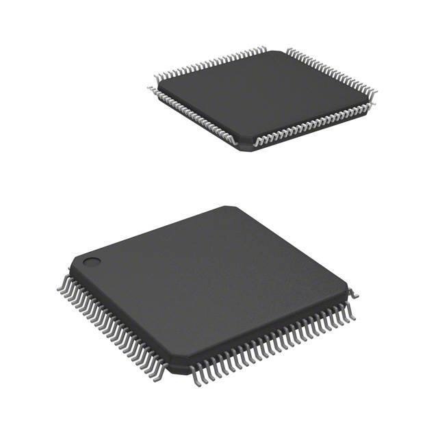
XRT5997IV
100-Lead TQFP (14 x 14 x 1.4 mm)
-40°C to +85°C
Rev. 1.0.0
EXAR Corporation, 48720 Kato Road, Fremont, CA 94538 • (510) 668-7000 • FAX (510) 668-7017 • www.exar.com
�XRT5997
Channel 7
Channel 6
Channel 5
Channel 4
RxLO S
Channel 3
Channel 2
Channe
l1
RTIP
RRing
Receiv
Receive
e
Equalizer
Equalizer
TTIP
Peak Peak
Detector/
Detector/
Slice
Slicer
r
LO
LOSS
Detecto
Detector
r
PulsePulse
Shaping
Shaping
Circuit
Circuit
TRing
Figure 1. XRT5997 Block Diagram
Rev. 1.0.0
2
Receive
Receive
O utput
O utput
Interfac
Interface
e
Transm
it
Transm
it Input
Input
Interface
Interface
RxPO S
RxNEG
TxPO S
TxNEG
TxClk
�XRT5997
TxClk6
TxPOS6
LOS6
77
76
80
TxNEG6
TGND6
81
78
TTIP6
82
79
TRing6
TVDD6
83
DGND
84
87
TxNEG7
TxClk7
88
TxPOS7
DGND
89
85
TTIP7
90
86
TRing7
TVDD7
91
TRing1
TGND7
92
TVDD1
TTIP1
93
94
TxClk1
97
95
TxNEG1
98
TGND1
TxPOS1
99
96
LOS1
100
PIN CONFIGURATION
R xPO S 1
1
75
R xN E G 1
R xPO S 6
2
74
R xN E G 6
DVDD
3
73
DGND
LO S7
4
72
AG N D
R xPO S 7
5
71
R T IP6
R xN E G 7
6
70
R R ing6
R T IP1
7
69
R T IP7
R R ing1
8
68
R R ing7
67
AV D D
66
AG N D
65
AV D D
AV D D
9
AG N D
10
AV D D
R R ing2
11
12
R T IP2
13
AG N D
14
T T IP2
100-Pin
TQFP
X RT 5997IV
15
TVDD2
16
T R ing2
17
64
R R ing5
63
R T IP5
62
TGND5
61
T T IP5
60
TVDD5
59
T R ing5
TGND4
TGND2
18
58
T R ing3
19
57
T R ing4
TVDD3
20
56
TVDD4
21
55
T T IP4
22
54
DGND
53
R T IP4
24
52
R R ing4
25
51
T xC lk4
Rev. 1.0.0
3
50
48
LOS4
49
47
RxPOS4
TxPOS4
46
TxNEG4
45
TxPOS5
44
100 LEAD THIN QUAD FLAT PACK
(14 x 14 x 1.4 mm., TQFP)
RxNEG4
43
42
RxNEG5
TxClk5
41
TxNEG5
40
37
DVDD
LOS5
36
LOS2
RxPOS5
35
RxPOS2
DGND
34
RxNEG2
39
33
TxClk2
38
32
DVDD
31
TxPOS2
TxNEG2
30
RxPOS3
RxNEG3
28
LOS3
29
27
T xC lk3
23
26
R T IP3
R R ing3
TxPOS3
TGND3
TxNEG3
T T IP3
�XRT5997
PIN DESCRIPTION
Pin#
Symbol
Type
1
RxPOS1
O
Description
Receiver 1 Positive Data Out:
This output pin will pulse “high” whenever Channel 1, within the XRT5997
device has received a “Positive Polarity” pulse, in the incoming line signal,
at RTIP1/RRing1 inputs.
2
RxNEG1
O
Receiver 1 Negative Data Out:
This output pin will pulse “high” whenever Channel 1, within the XRT5997
device has received a “Negative Polarity” pulse, in the incoming line signal,
at tRTIP1/RRing1 inputs.
3
DVDD
-
Positive Supply - (+3.3V ± 5%). Digital Circuitry.
4
LOS7
O
Receiver 7 Loss of Signal Output Indicator:
This output pin toggles “high” if Channel 7, within the XRT5997 device has
detected a “Loss of Signal” condition in the incoming line signal.
5
RxPOS7
O
Receiver 7 Positive Data Out:
This output pin will pulse “high” whenever Channel 7, within the XRT5997
device has received a “Positive Polarity” pulse, in the incoming line signal,
at RTIP7/RRing7 inputs.
6
RxNEG7
O
Receiver 7 Negative Data Out:
This output pin will pulse “high” whenever Channel 7, within the XRT5997
device has received a “Negative Polarity” pulse, in the incoming line signal,
at RTIP7/RRing7 inputs.
7
RTIP1
I
Receiver 1 Positive Bipolar Input:
The Receive Section of Channel 1 uses this input pin, along with RRing1
to receive the bipolar line signal from the “Remote E1 Terminal”.
8
RRing1
I
Receiver 1 Negative Bipolar Input:
The Receive Section of Channel 1 uses this input pin, along with RTIP1 to
receive the bipolar line signal from the “Remote E1 Terminal”.
9
AVDD
-
Positive Supply - (+3.3V ± 5%). Analog Circuitry.
10
AGND
-
Analog Ground
11
AVDD
12
RRing2
I
Receiver 2 Negative Bipolar Input:
The Receive Section of Channel 2 uses this input pin, along with RTIP2 to
receive the bipolar line signal from the “Remote E1 Terminal”.
13
RTIP2
I
Receiver 2 Positive Bipolar Input:
The Receive Section of Channel 2 uses this input pin, along with RRing2
to receive the bipolar line signal from the “Remote E1 Terminal”.
Positive Supply - (+3.3V ± 5%). Receiver 1, 2, 3, 5.
Rev. 1.0.0
4
�XRT5997
PIN DESCRIPTION (CONT'D)
Pin#
Symbol
Type
Description
14
AGND
-
Analog Ground - Receiver 1, 2, 3, 5.
15
TTIP2
O
Transmitter 2 Positive Bipolar Output:
Channel 2 within the XRT5997 device will use this pin, along with TRing2,
to transmit a bipolar line signal, via a 1:2 step-up transformer.
16
TVDD2
-
Positive Supply - (+3.3V ± 5%), Transmitters 2.
17
TRing2
O
Transmitter 2 Negative Bipolar Output:
Channel 2 within the XRT5997 device will use this pin, along with TTIP2, to
transmit a bipolar line signal, via a 1:2 step-up transformer.
18
TGND2
Digital Ground - Transmitters 2.
19
TRing3
20
TVDD3
21
TTIP3
22
TGND3
23
RTIP3
I
Receiver 3 Positive Bipolar Input.
The Receive Section of Channel 4 uses this input pin, along with RRing3
to receive the bipolar line signal from the “Remote E1 Terminal”.
24
RRing3
I
Receiver 3 Negative Bipolar Input.
The Receive Section of Channel 3 uses this input pin, along with RTIP3 to
receive the bipolar line signal from the “Remote E1 Terminal”.
25
TxClk3
I
Transmitter Clock Input – Channel 3:
If the user operates Channel 3 (within the XRT5997 device) in the “clocked”
mode, then the “Transmit Section” of the Channel 3 will use the falling edge
of this signal to sample the data at the TxPOS3 and TxNEG3 input pins.
O
Transmitter 3 Negative Bipolar Output:
Channel 3 within the XRT5997 device will use this pin, along with TTIP3, to
transmit a bipolar line signal, via a 1:2 step-up transformer.
Positive Supply - (+3.3V ± 5%), Transmitters 3.
O
Transmitter 3 Positive Bipolar Output:
Channel 3 within the XRT5997 device will use this pin, along with TRing3,
to transmit a bipolar line signal, via a 1:2 step-up transformer.
Digital Ground - Transmitters 3.
Note: If the user operates the Channel 3 in the “clockless” mode, then the
Terminal Equipment should not apply a clock signal to this input pin.
Rev. 1.0.0
5
�XRT5997
PIN DESCRIPTION (CONT'D)
Pin#
Symbol
Type
26
TxNEG3
I
Description
Transmitter - Negative Data Input – Channel 3:
The exact signal that should be applied to this input pin depends upon
whether the user intends to operate the “Transmit Section” (of Channel 3) in
the “Clocked” or “Clockless” Mode.
Clocked Mode:
The Terminal Equipment should apply bit-wide NRZ pulses on this input
pin, whenever the Terminal Equipment needs to transmit a “negativepolarity” pulse onto the line via TTIP3 and TRing3 output pins. The
XRT5997 device will sample this input pin upon the falling edge of the
TClk3 signal.
Clockless Mode:
The Terminal Equipment should apply RZ pulses to this input pin, anytime
the Terminal Equipment needs to transmit a “negative-polarity” pulse onto
the line viaTTIP3 and TRing3 output pins.
27
TxPOS3
I
Transmitter - Positive Data Input – Channel 3:
The exact signal that should be applied to this input pin depends upon
whether the user intends to operate the “Transmit Section” (of Channel 3) in
the “Clocked” or “Clockless” Mode.
Clocked Mode:
The Terminal Equipment should apply bit-wide NRZ pulses on this input
pin, whenever the Terminal Equipment needs to transmit a “positivepolarity” pulse onto the line via TTIP1 and TRing1 output pins. The
XRT5997 device will sample this input pin upon the falling edge of the
TClk1 signal.
Clockless Mode:
The Terminal Equipment should apply RZ pulses to this input pin, anytime
the Terminal Equipment needs to transmit a “positive-polarity” pulse onto the
line via TTIP1 and TRing1 output pins).
28
LOS3
O
Receiver 3 – Loss of Signal Output Indicator:
This output pin toggles “high” if Channel 3, within the XRT5997 device has
detected a “Loss of Signal” condition in the incoming line signal.
29
RxPOS3
O
Receiver 3 Positive Data Out:
This output pin will pulse “high” whenever Channel 3, within the XRT5997
device has received a “Positive Polarity” pulse, in the incoming line signal, at
RTIP3/RRing3 inputs.
Rev. 1.0.0
6
�XRT5997
PIN DESCRIPTION (CONT'D)
Pin#
Symbol
Type
Description
30
RxNEG3
O
Receiver 3 Negative Data Out:
This output pin will pulse “high” whenever Channel 3, within the XRT5997
device has received a “Negative Polarity” pulse, in the incoming line signal,
at RTIP3/RRing3 inputs.
31
TxPOS2
I
Transmitter - Positive Data Input – Channel 2:
The exact signal that should be applied to this input pin depends upon
whether the user intends to operate the “Transmit Section” (of Channel 2) in
the “Clocked” or “Clockless” Mode.
Clocked Mode:
The Terminal Equipment should apply bit-wide NRZ pulses on this input pin,
whenever the Terminal Equipment needs to transmit a “positive-polarity”
pulse onto the line via TTIP2 and TRing2 output pins). The XRT5997
device will sample this input pin upon the falling edge of the TClk2 signal.
Clockless Mode:
The Terminal Equipment should apply RZ pulses to this input pin, anytime
the Terminal Equipment needs to transmit a “positive-polarity” pulse onto the
line via TTIP2 and TRing2 output pins.
32
TxNEG2
I
Transmitter - Negative Data Input – Channel 2:
The exact signal that should be applied to this input pin depends upon
whether the user intends to operate the “Transmit Section” (of the Channel 2)
in the “Clocked” or “Clockless” Mode.
Clocked Mode:
The Terminal Equipment should apply bit-wide NRZ pulses on this input pin,
whenever the Terminal Equipment needs to transmit a “negative-polarity”
pulse onto the line via TTIP2 and TRing2 output pins. The XRT5997
device will sample this input pin upon the falling edge of the TClk2 signal.
Clockless Mode:
The Terminal Equipment should apply RZ pulses to this input pin, anytime the
Terminal Equipment needs to transmit a “negative-polarity” pulse onto the
line via TTIP2 and TRing2 output pins.
33
TxClk2
I
Transmitter Clock Input – Channel 2:
If the user operates Channel 2 (within the XRT5997 device) in the “clocked”
mode, then the “Transmit Section” of the Channel 2 will use the falling edge
of this signal to sample the data at the TxPOS2 and TxNEG2 input pins.
Note If the user operates the Channel 2 in the “clockless” mode, then the
Terminal Equipment should not apply a clock signal to this input pin.
Note:
1
Internally pull-up with 50K resistor.
Rev. 1.0.0
7
�XRT5997
PIN DESCRIPTION (CONT'D)
Pin#
Symbol
Type
Description
34
RxNEG2
O
Receiver 2 Negative Data Out:
This output pin will pulse “high” whenever Channel 2, within the XRT5997
device has received a “Negative Polarity” pulse, in the incoming line signal,
at RTIP2/RRing2 inputs.
35
RxPOS2
O
Receiver 2 Positive Data Out:
This output pin will pulse “high” whenever Channel 2, within the XRT5997
device has received a “Positive Polarity” pulse, in the incoming line signal, at
RTIP2/RRing2 inputs.
36
LOS2
O
Receiver 2 Loss of Signal:
This output pin toggles “high” if Channel 2, within the XRT5997 device has
detected a “Loss of Signal” condition in the incoming line signal.
37
DVDD
-
Positive Supply (+3.3V ± 5%). Digital Circuitry.
38
DVDD
-
Positive Supply (+3.3V ± 5%). Digital Circuitry.
39
DGND
-
Digital Ground: Digital Circuitry.
40
LOS5
O
Receiver 5 Loss of Signal:
This output pin toggles “high” if Channel 5, within the XRT5997 device has
detected a “Loss of Signal” condition in the incoming line signal.
Note: 1Internally pull-up with 50K resistor
41
RxPOS5
O
Receiver 5 Positive Data Out:
This output pin will pulse “high” whenever Channel 5, within the XRT5997
device has received a “Positive Polarity” pulse, in the incoming line signal, at
RTIP5/RRing5 inputs.
42
RxNEG5
O
Receiver 5 Negative Data Out:
This output pin will pulse “high” whenever Channel 5, within the XRT5997
device has received a “Negative Polarity” pulse, in the incoming line signal,
at RTIP5/RRing5 inputs.
43
TxClk5
I
Transmitter Clock Input – Channel 5:
If the user operates Channel 5 (within the XRT5997 device) in the “clocked”
mode, then the “Transmit Section” of the Channel 5 will use the falling edge of
this signal to sample the data at the TxPOS5 and TxNEG5 input pins.
NOTE: If the user operates the Channel 5 in the “clockless” mode, then the
Terminal Equipment should not apply a clock signal to this input pin.
Note:
1
Internally pull-up with 50K resistor.
Rev. 1.0.0
8
�XRT5997
PIN DESCRIPTION (CONT'D)
Pin#
Symbol
Type
44
TxNEG5
I
Description
Transmitter - Negative Data Input – Channel 5:
The exact signal that should be applied to this input pin depends upon
whether the user intends to operate the “Transmit Section” (of the Channel 5)
in “Clocked” or “Clockless” Mode.
Clocked Mode:
The Terminal Equipment should apply bit-wide NRZ pulses on this input pin,
whenever the Terminal Equipment needs to transmit a “negative-polarity”
pulse onto the line via TTIP5 and TRing5 output pins. The XRT5997
device will sample this input pin upon the falling edge of the TCLK5 signal.
Clockless Mode:
The Terminal Equipment should apply RZ pulses to this input pin, anytime
the Terminal Equipment needs to transmit a “negative-polarity” pulse onto the
line via TTIP5 and TRing5 output pins.
45
TxPOS5
I
Transmitter - Positive Data Input – Channel 5:
The exact signal that should be applied to this input pin depends upon
whether the user intends to operate the “Transmit Section” (of Channel 5) in
the “Clocked” or “Clockless” Mode.
Clocked Mode:
The Terminal Equipment should apply bit-wide NRZ pulses on this input pin,
whenever the Terminal Equipment needs to transmit a “positive-polarity”
pulse onto the line via TTIP5 and TRing5 output pins. The XRT5997
device will sample this input pin upon the falling edge of the TClk5 signal.
Clockless Mode:
The Terminal Equipment should apply RZ pulses to this input pin, anytime the
Terminal Equipment needs to transmit a “positive-polarity” pulse onto the line
via TTIP5 and TRing5 output pins.
46
RxNEG4
O
Receiver 4 Negative Data Out:
This output pin will pulse “high” whenever Channel 4, within the XRT5997
device has received a “Negative Polarity” pulse, in the incoming line signal,
at the RTIP4/RRing4 inputs.
47
RxPOS4
O
Receiver 4 Positive Data Out:
This output pin will pulse “high” whenever Channel 4, within the XRT5997
device has received a “Positive Polarity” pulse, in the incoming line signal, at
RTIP4/RRing4 inputs.
Rev. 1.0.0
9
�XRT5997
PIN DESCRIPTION (CONT'D)
Pin#
Symbol
Type
Description
48
LOS4
O
Receiver 4 Loss of Signal:
This output pin toggles “high” if Channel 4, within the XRT5997 device has
detected a “Loss of Signal” condition in the incoming line signal.
49
TxPOS4
O
Transmitter - Positive Data Input – Channel 4:
The exact signal that should be applied to this input pin depends upon
whether the user intends to operate the “Transmit Section” (of Channel 4) in
the “Clocked” or “Clockless” Mode.
Clocked Mode:
The Terminal Equipment should apply bit-wide NRZ pulses on this input pin,
whenever the Terminal Equipment needs to transmit a “positive-polarity”
pulse onto the line via TTIP4 and TRing4 output pins). The XRT5997
device will sample this input pin upon the falling edge of the TClk4 signal.
Clockless Mode:
The Terminal Equipment should apply RZ pulses to this input pin, anytime
the Terminal Equipment needs to transmit a “positive-polarity” pulse onto the
line via TTIP4 and TRing4 output pins.
50
TxNEG4
I
Transmitter - Negative Data Input – Channel 4:
The exact signal that should be applied to this input pin depends upon
whether the user intends to operate the “Transmit Section” (of the Channel 4)
in the “Clocked” or “Clockless” Mode.
In the Clocked Mode:
The Terminal Equipment should apply bit-wide NRZ pulses on this input pin,
whenever the Terminal Equipment needs to transmit a “negative-polarity”
pulse onto the line via the TTIP4 and TRing4 output pins. The XRT5997
device will sample this input pin upon the falling edge of the TClk4 signal.
In the Clockless Mode:
The Terminal Equipment should apply RZ pulses to this input pin, anytime the
Terminal Equipment needs to transmit a “negative-polarity” pulse onto the
line (via the TTIP4 and TRing4 output pins).
51
TxClk4
I
Transmitter Clock Input – Channel 4:
If the user operates Channel 4 (within the XRT5997 device) in the “clocked”
mode, then the “Transmit Section” of the Channel 4 will use the falling edge of
this signal to sample the data at the TxPOS4 and TxNEG4 input pins.
Note: If the user operates the Channel 4 in the “clockless” mode, then the
Terminal Equipment should not apply a clock signal to this input pin.
52
RRing4
I
Receiver 4 Negative Bipolar Input:
The Receive Section of Channel 4 uses this input pin, along with RTIP4 to
receive the bipolar line signal from the “Remote E1 Terminal”.
Rev. 1.0.0
10
�XRT5997
PIN DESCRIPTION (CONT'D)
Pin#
Symbol
Type
Description
53
RTIP4
I
54
DGND
55
TTIP4
56
TVDD4
57
TRing4
58
TGND4
59
TRing5
60
TVDD5
61
TTIP5
62
TGND5
63
RTIP5
I
64
RRing5
I
65
AVDD
Positive Supply (+3.3V ± 5%). Analog Circuitry.
66
AGND
Analog Ground.
67
AVDD
Positive Supply (+3.3V ± 5%). Receiver 4, 6, 7.
68
RRing7
Receiver 4 Positive Bipolar Input.
The Receive Section of Channel 4 uses this input pin, along with RRing4 to
receive the bipolar line signal from the “Remote E1 Terminal”.
Digital Ground. Digital Circuitry.
O
Transmitter 4 Positive Bipolar Output.
Channel 4 within the XRT5997 device will use this pin, along with TRing4, to
transmit a bipolar line signal, via a 1:2 step-up transformer.
Positive Supply (+3.3V ± 5%), Transmitters 4.
O
Transmitter 4 Negative Bipolar Output.
Channel 4 within the XRT5997 device will use this pin, along with TTIP4, to
transmit a bipolar line signal, via a 1:2 step-up transformer.
Digital Ground. Transmitters 4.
O
Transmitter 5 Negative Bipolar Output.
Channel 5 within the XRT5997 device will use this pin, along with TTIP5, to
transmit a bipolar line signal, via a 1:2 step-up transformer.
Positive Supply (+3.3V ± 5%), Transmitters 5.
O
Transmitter 5 Positive Bipolar Output.
Channel 5 within the XRT5997 device will use this pin, along with TRing5, to
transmit a bipolar line signal, via a 1:2 step-up transformer.
Digital Ground. Transmitters 5.
I
Receiver 5 Positive Bipolar Input.
The Receive Section of Channel 5 uses this input pin, along with RRing5 to
receive the bipolar line signal from the “Remote E1 Terminal”.
Receiver 5 Negative Bipolar Input.
The Receive Section of Channel 5 uses this input pin, along with RTIP5 to
receive the bipolar line signal from the “Remote E1 Terminal”.
Receiver 7 Negative Bipolar Input.
The Receive Section of Channel 7 uses this input pin, along with RTIP7 to
receive the bipolar line signal from the “Remote E1 Terminal”.
Rev. 1.0.0
11
�XRT5997
PIN DESCRIPTION (CONT'D)
Pin#
Symbol
Type
Description
69
RTIP7
I
Receiver 7 Positive Bipolar Input:
The Receive Section of Channel 7 uses this input pin, along with RRing7 to
receive the bipolar line signal from the “Remote E1 Terminal”.
70
RRing6
I
Receiver 6 Negative Bipolar Input:
The Receive Section of Channel 6 uses this input pin, along with RTIP6 to
receive the bipolar line signal from the “Remote E1 Terminal”.
71
RTIP6
I
Receiver 6 Positive Bipolar Input:
The Receive Section of Channel 6 uses this input pin, along with RRing6 to
receive the bipolar line signal from the “Remote E1 Terminal”.
72
AGND
Analog Ground. Receiver 4, 6, 7.
73
DGND3
Digital Ground. Digital Circuitry.
74
RxNEG6
O
Receiver 6 Negative Data Out:
This output pin will pulse “high” whenever Channel 6, within the XRT5997
device has received a “Negative Polarity” pulse, in the incoming line signal,
at RTIP6/RRing6 inputs.
75
RxPOS6
O
Receiver 6 Positive Data Out:
This output pin will pulse “high” whenever Channel 6, within the XRT5997
device has received a “Positive Polarity” pulse, in the incoming line signal, at
RTIP6/RRing6 inputs.
76
LOS6
O
77
TxPOS6
I
Receiver 6 Loss of Signal:
This output pin toggles “high” if Channel 6, within the XRT5997 device has
detected a “Loss of Signal” condition in the incoming line signal.
Transmitter - Positive Data Input – Channel 6:
The exact signal that should be applied to this input pin depends upon
whether the user intends to operate the “Transmit Section” (of Channel 6) in
the “Clocked” or “Clockless” Mode.
Clocked Mode:
The Terminal Equipment should apply bit-wide NRZ pulses on this input pin,
whenever the Terminal Equipment needs to transmit a “positive-polarity”
pulse onto the line via TTIP6 and TRing6 output pins. The XRT5997
device will sample this input pin upon the falling edge of the TClk6 signal.
Clockless Mode:
The Terminal Equipment should apply RZ pulses to this input pin, anytime the
Terminal Equipment needs to transmit a “positive-polarity” pulse onto the line
via TTIP6 and TRing6 output pins.
Rev. 1.0.0
12
�XRT5997
PIN DESCRIPTION (CONT'D)
Pin#
Symbol
Type
78
TxNEG6
I
Description
Transmitter - Negative Data Input – Channel 6:
The exact signal that should be applied to this input pin depends upon
whether the user intends to operate the “Transmit Section” (of the Channel 6)
in the “Clocked” or “Clockless” Mode.
Clocked Mode:
The Terminal Equipment should apply bit-wide NRZ pulses on this input pin,
whenever the Terminal Equipment needs to transmit a “negative-polarity”
pulse onto the line via TTIP6 and TRing6 output pins. The XRT5997
device will sample this input pin upon the falling edge of the TClk6 signal.
Clockless Mode:
The Terminal Equipment should apply RZ pulses to this input pin, anytime the
Terminal Equipment needs to transmit a “negative-polarity” pulse onto the
line via TIP6 and TRing6 output pins.
79
TxClk6
I
Transmitter Clock Input – Channel 6:
If the user operates Channel 6 (within the XRT5997 device) in the “clocked”
mode, then the “Transmit Section” of the Channel 6 will use the falling edge of
this signal to sample the data at the TxPOS6 and TxNEG6 input pins.
Note: If the user operates the Channel 6 in the “clockless” mode, then the
Terminal Equipment should not apply a clock signal to this input pin.
80
TGND6
81
TTIP6
82
TVDD6
83
TRing6
84
DGND
Digital Ground. Transmitters 6.
O
Transmitter 6 Positive Bipolar Output:
Channel 6 within the XRT5997 device will use this pin, along with TRing6, to
transmit a bipolar line signal, via a 1:2 step-up transformer.
Positive Supply (+3.3V ± 5%), Transmitters 6.
O
Transmitter 6 Negative Bipolar Output:
Channel 6 within the XRT5997 device will use this pin, along with TTIP6, to
transmit a bipolar line signal, via a 1:2 step-up transformer.
Digital Ground. Digital Circuitry.
Rev. 1.0.0
13
�XRT5997
PIN DESCRIPTION (CONT'D)
Pin#
Symbol
Type
85
TxPOS7
I
Description
Transmitter - Positive Data Input – Channel 7:
The exact signal that should be applied to this input pin depends upon
whether the user intends to operate the “Transmit Section” (of Channel 7) in
the “Clocked” or “Clockless” Mode.
Clocked Mode:
The Terminal Equipment should apply bit-wide NRZ pulses on this input pin,
whenever the Terminal Equipment needs to transmit a “positive-polarity”
pulse onto the line via TTIP7 and TRing7 output pins. The XRT5997
device will sample this input pin upon the falling edge of the TClk7 signal.
Clockless Mode:
The Terminal Equipment should apply RZ pulses to this input pin, anytime the
Terminal Equipment needs to transmit a “positive-polarity” pulse onto the line
via TTIP7 and TRing7 output pins.
86
TxNEG7
I
Transmitter - Negative Data Input – Channel 7:
87
TxClk7
I
Transmitter Clock Input – Channel 7:
If the user operates Channel 7 (within the XRT5997 device) in the “clocked”
mode, then the “Transmit Section” of the Channel 7 will use the falling edge of
this signal to sample the data at the TxPOS7 and TxNEG7 input pins.
Note: If the user operates the Channel 7 in the “clockless” mode, then the
Terminal Equipment should not apply a clock signal to this input pin.
88
DGND
89
TTIP7
90
TVDD7
91
TRing7
92
TGND7
93
TRing1
94
TVDD1
Digital Ground: Digital Circuitry.
O
Transmitter 7 Positive Bipolar Output:
Channel 7 within the XRT5997 device will use this pin, along with TRing7, to
transmit a bipolar line signal, via a 1:2 step-up transformer.
Positive Supply: (+3.3V ± 5%), Transmitters 7.
O
Transmitter 7 Negative Bipolar Output:
Channel 7 within the XRT5997 device will use this pin, along with TTIP7, to
transmit a bipolar line signal, via a 1:2 step-up transformer.
Digital Ground: Transmitters 7.
O
Transmitter 1 Negative Bipolar Output:
Channel 1 within the XRT5997 device will use this pin, along with TTIP1, to
transmit a bipolar line signal, via a 1:2 step-up transformer.
Positive Supply (+3.3V ± 5%), Transmitters 1.
Rev. 1.0.0
14
�XRT5997
PIN DESCRIPTION (CONT'D)
Pin#
Symbol
Type
95
TTIP1
O
96
TGND1
97
TxClk1
Description
Transmitter 1 Positive Bipolar Output.
Channel 1 within the XRT5997 device will use this pin, along with TRing1, to
transmit a bipolar line signal, via a 1:2 step-up transformer.
Digital Ground. Transmitters 1.
I
Transmitter Clock Input – Channel 1:
If the user operates Channel 1 (within the XRT5997 device) in the “clocked”
mode, then the “Transmit Section” of the Channel 1 will use the falling edge of
this signal to sample the data at the TxPOS1 and TxNEG1 input pins.
Note: If the user operates the Channel 1 in the “clockless” mode, then the
Terminal Equipment should not apply a clock signal to this input pin..
98
TxNEG1
I
Transmitter - Negative Data Input – Channel 1:
The exact signal that should be applied to this input pin depends upon
whether the user intends to operate the “Transmit Section” (of the Channel 1)
in the “Clocked” or “Clockless” Mode.
Clocked Mode:
The Terminal Equipment should apply bit-wide NRZ pulses on this input pin,
whenever the Terminal Equipment needs to transmit a “negative-polarity”
pulse onto the line via TTIP1 and TRing1 output pins. The XRT5997
device will sample this input pin upon the falling edge of the TClk1 signal.
Clockless Mode:
The Terminal Equipment should apply RZ pulses to this input pin, anytime the
Terminal Equipment needs to transmit a “negative-polarity” pulse onto the
line via TTIP1 and TRing1 output pins.
99
TxPOS1
I
Transmitter - Positive Data Input – Channel 1:
The exact signal that should be applied to this input pin depends upon
whether the user intends to operate the “Transmit Section” (of Channel 1) in
the “Clocked” or “Clockless” Mode.
Clocked Mode:
The Terminal Equipment should apply bit-wide NRZ pulses on this input pin,
whenever the Terminal Equipment needs to transmit a “positive-polarity”
pulse onto the line via TTIP1 and TRing1 output pins. The XRT5997
device will sample this input pin upon the falling edge of the TClk1 signal.
Clockless Mode:
The Terminal Equipment should apply RZ pulses to this input pin, anytime the
Terminal Equipment needs to transmit a “positive-polarity” pulse onto the line
via TTIP1 and TRing1 output pins.
100
LOS1
O
Receiver 1 Loss of Signal:
This output pin toggles “high” if Channel 1, within the XRT5997 device has
detected a “Loss of Signal” condition in the incoming line signal.
Rev. 1.0.0
15
�XRT5997
RECEIVER ELECTRICAL CHARACTERISTICS
Unless otherwise specified: TA=-40 to 85°C, VDD=3.3V±5%, unless otherwise specified.
Parameter
Min
Typ
Max
Unit
Test Conditions
Threshold to Assert
12
20
-
dB
Threshold to Clear
11
15
Time Delay
10
-
255
bit
Hysteresis
-
5
-
dB
Receiver Sensitivity
11
13
-
dB
Below nominal pulse amplitude of 3.0V
for 120Ω and 2.37V for 75Ω applications.
With -18dB interference signal added.
Interference Margin
-18
-14
-
dB
With 6dB cable loss.
5
-
-
KΩ
-
-
UIpp
Receiver Loss of Signal:
Input Impedance
Cable attenuation @ 1024KHz
dB
Per ITU-G.775
Jitter Tolerance:
20Hz
10
700Hz
5
10KHz —100KHz
0.3
Return Loss:
51KHz —102KHz
14
-
-
dB
102KHz—2048KHz
20
-
-
dB
2048KHz—3072KHz
16
-
-
dB
Per ITU-G.703
TRANSMITTER ELECTRICAL CHARACTERISTICS
Unless otherwise specified: TA=-40 to 85°C, VDD=3.3V±5%, unless otherwise specified.
Parameter
Min
Typ
Max
Unit
2.13
2.70
2.37
3.0
2.60
3.30
V
V
Output Pulse Width
224
244
264
ns
Output Pulse Width Ratio
0.95
Output Pulse Amplitude Ratio
Output Return Loss:
51KHz —102KHz
102KHz—2048KHz
2048KHz—3072KHz
0.95
−
−
10
16
12
-
Test Conditions
AMI Output Pulse Amplitude:
75Ω Application
120Ω Application
1.05
−
−
-
dB
dB
dB
1.05
Rev. 1.0.0
16
Use transformer with 1:2 ratio and 9.1Ω
resistor in series with each end of primary.
Per ITU-G.703
Per ITU-G.703
Per ETSI 300 166 and CH PTT
�XRT5997
269ns
244+50
V= 100 %
194ns
244-50
Normal Pulse
50 %
244 ns
219 ns
244-25
0%
20 %
244 ns
244+244
Figure E1. ITU G.703 Pulse Template for Transmitter Output
DC ELECTRICAL CHARACTERISTICS
TA=-25°C, VDD=3.3V±5%, unless otherwise specified.
Parameter
Symbol
Min
Power Supply Voltage
VDD
3.13
3.3
3.46
V
Input High Voltage
Input Low Voltage
Output High Voltage @
IOH=-5mA
Output Low Voltage @
IOL=5mA
Input Leakage Current
(except Input pins w/ pull-up resistor.)
Input Capacitance
Output Load Capacitance
VIH
VIL
2.0
-0.5
-
5.0
0.8
V
V
VOH
2.4
-
-
V
VOL
IL
-
-
0.4
± 10
V
µA
CI
CL
-
5.0
-
25
pF
pF
Rev. 1.0.0
17
Typ
Max
Unit
�XRT5997
AC ELECTRICAL CHARACTERISTICS
TA=-25°C, VDD=3.3V±5%, unless otherwise specified.
Parameter
Symbol
Min
Typ
Max
Unit
T1
-
488
-
ns
TCLK Duty Cycle
T2
47
50
53
%
Transmit Data Setup Time
TSU
50
-
-
ns
Transmit Data Hold Time
THO
30
-
-
ns
Transmit Data Prop. Delay Time
T3
-
30
-
ns
TCLK Clock Period
- RZ data Mode
- NRZ data Mode (clock mode)
TCLK Rise Time(10%/90%)
TCLK Fall Time(90%/10%)
-
30
-
ns
TR
-
-
40
ns
TF
-
-
40
ns
Rtr
-
-
40
ns
Receive Data Fall Time
Rtf
-
-
40
ns
Receive Data Prop. Delay
Rpd
-
75
-
ns
Receive Data Pulse Width
Rxpw
200
244
350
ns
Receive Data Rise Time
Per channel power consumption including the line power dissipation, tranmission and receive paths
all active: TA=-40 to 85°C, VDD=3.3V±5%, unless otherwise specified.
Parameter
Symbol
Min
Typ
Max
Unit
Conditions
Power Consumption
Power Consumption
Power Consumption
PC
PC
PC
-
85
72
135
95
80
144
mW
mW
mW
75Ω load, operating at 50% Mark Density.
120Ω load, operating at 50% Mark Density.
75Ω load, operating at 100% Mark Density.
Power Consumption
Power Consumption
PC
PC
-
106
16
115
18
mW
mW
120Ω load, operating at 100% Mark Density.
Transmitter in Powered-down mode.
ABSOLUTE MAXIMUM RATINGS
Storage Temperature
Operating Temperature
ESD Rating
Supply Voltage
○
○
○
○
○
Note:
2
○
○
○
○
○
○
○
○
○
○
○
○
○
○
○
○
○
○
○
○
○
○
○
○
○
○
○
○
-65°C to + 150°C
-40°C to + 85°C
>4000V on all pins2
-0.5V to + 6.0V
○
○
○
○
○
Human Body Model, 100pF capacitor discharged through a 1.5KΩ resistor.
Rev. 1.0.0
18
�XRT5997
SYSTEM DESCRIPTION
1.1
The Transmit Input Interface
The XRT5997 device is a Seven (7) channel E1
transceiver that provides an electrical interface for
2.048Mbps applications. Each of the seven channels
includes a receive circuit that converts an ITU-T G.703
compliant bipolar signal into a TTL compatible logic
levels. Each receiver also includes an LOS (Loss of
Signal) detection circuit. Similarly, in the Transmit
Direction, each Transmitter converts TTL compatible
logic levels into a G.703 compatible bipolar signal.
The Transmitter may be operated in either a “Clocked”
or “Clockless” Mode.
The Transmit Input Interface accepts either “clocked”
or “clockless” data from the Terminal Equipment. The
manner in how the Terminal Equipment should apply
data to a given channel within the XRT5997 device
depends upon whether the channel is being operated in
the “clocked” or “clockless” mode.
1.2.1 Operating the Transmitter in the Clocked
Mode
The user can configure a given channel (within the
XRT5997 device) to operate in the “Clocked” mode by
simply applying a 2.048MHz clock signal to the
“TxClk_x” input pin (where x denotes a given channel
within the XR5997 device). The XRT5997 device
contains some circuitry that sense activity on the
“TxClk_x” line. If this circuit senses activity on the
“TxClk_x” line, then the corresponding channel will
automatically be operating in the “Clocked” Mode.
Each channel within the XRT5997 LIU device consists
of both a Transmit Section and a Receive Section,
each of these sections will be discussed in detail
below.
1.0 The Transmit Section
In general, the purpose of the “Transmit Section”
(within each channel of the XRT5997 device) is to
accept TTL/CMOS level digital data (from the Terminal
Equipment), and to encode it into a format such that it
can:
In the Clocked Mode, the Terminal Equipment is
expected to apply a 2.048MHz clock signal at the
TxClk_x input pin and NRZ data at the TxPOS_x and
TxNEG_x input pins. The “Transmit Input Interface”
circuit will sample the data, at the TxPOS_x and
TxNEG_x input pins, upon the falling edge of TxClk_x,
as illustrated in Figure 3.
1. Be efficiently transmitted over coaxial- or twistedpair cable at the E1 data rate; and
2. Be reliably received by the Remote Terminal
Equipment at the other end of the E1 data link.
3. Comply with the ITU-T G.703 pulse template
requirements, for E1 applications.
The circuitry that the Transmit Section (within the
XRT5997 device) uses to accomplish this goal is
discussed below. The Transmit Section of the
XRT5997 device consists of the following blocks:
• Transmit Input Interface
• Pulse Shaping Block
Rev. 1.0.0
19
�XRT5997
tS U
tH O
TxP O S _x
TxN E G _x
TC lk_x
Figure 2. Illustration on how the XRT5997 Device Samples the data on
the TxPOS_x and TxNEG_x input pins
In general, if the XRT5997 device samples a “1” on the
TxPOS_x input pin, then the “Transmit Section” of the
device will ultimately generate a positive polarity pulse
via the TTIP_x and TRing_x output pins (across a 1:2
transformer). Conversely, if the XRT5997 device
samples a “1” on the “TxNEG_x” input pin, then the
“Transmit Section” of the device will ultimately generate a negative polarity pulse via the TTIP_x and TRing_x
output pins (across a 1:2 transformer).
1.2.1
Operating the Transmitter in the
“Clockless” Mode
The user can configure a given channel (within the
XRT5997 device) to operate in the “Clockless” mode by
doing the following:
• Not applying a clock signal to the TxClk_x input,
and either pulling this pin to VDD or letting it float.
• By applying RZ (Return to Zero) data to the
TxPOS_x and TxNEG_x input pins, as illustrated
below.
Rev. 1.0.0
20
�XRT5997
B it
P e rio d
Data
1
RZ P ulse is to be
applied in the first
half of the bit-period
1
No pulse is to be applied
in the second half of the
bit period
0
1
1
0
1
TxPO S _x
TxNEG _x
TxClk _x
No Activity in TxClk Line
Figure 3. Illustration on how the Terminal Equipment should apply data to the “Transmit Section” of a
given Channel (within the XRT5997 Device), when operating in the “Clockless” Mode
Figure 3, indicates that when the user is operating a
channel in the “Clockless” Mode, then the corresponding Terminal Equipment must do the following:
1.3
The Pulse Shaping Circuit
The purpose of the “Transmit Pulse Shaping” circuit is
to generate “Transmit Output” pulses that comply with
the ITU-T G.703 Pulse Template Requirements for E1
Applications.
• Not apply a signal on the “TxClk_x” line.
• When applying a pulse (to either the TxPOS_x or
TxNEG_x input pin), apply an RZ pulse to the
appropriate input pin. This RZ pulse should only
have a width of one-half the bit-period. Addition,
the RZ pulse should occupy only the first half of
the bit-period. The TxPOS_x and TxNEG_x input
pins must be at 0V, during the second half of
every bit-period.
Rev. 1.0.0
21
�XRT5997
269ns
(244 + 25)
194ns
V = 100%
Nominal Pulse
50%
244ns
219ns
(244 - 25)
10%
0%
10%
20%
Figure 4. Illustration of the ITU-T G.703 Pulse Template for E1 Applications
However, in both applications (e.g., 75Ω or 120Ω), the
user is advised to interface the Transmitter to the Line,
in the manner as depicted in Figures 5 and 6, respectively.
As a consequence, each channel (within the XRT5997
device) will take each mark (which is provided to it via
the “Transmit Input Interface” block, and will generate
a pulse that complies with the pulse template, presented in Figure 4, (when measured on the secondaryside of the Transmit Output Transformer).
1.4
Interfacing the Transmit Sections of the
XRT5997 device to the Line
ITU-T G.703 specifies that the E1 line signal can be
transmitted over coaxial cable and terminated with 75Ω
or transmitted over twisted-pair and terminated with
120Ω.
Rev. 1.0.0
22
�XRT5997
U1
99
TxPOS_1
TxPOS_1
1
95
R1
2
J1
TTIP_1
9.1
BNC
1
1:2
5
1
98
TxNEG_1
TxNEG_1
2
4
8
PE-65835
1
93
R2
2
TRING_1
9.1
97
TxLineClk_1
TxCLK_1
XRT5997
Figure 5. Illustration of how to interface the Transmit Sections of the
Ω ” Applications)
XRT5997 device to the Line (for “75Ω
U1
99
TxPOS_1
TxPOS_1
95
1
R1
2
TTIP_1
9.1
1
TxNEG_1
1:2
5
TTIP_Channel_1
98
TxNEG_1
4
8
TRing_Channel_1
PE-65835
1
93
R2
2
TRing_1
9.1
TxLineClk_1
97
TxClk_1
XRT5997
Figure 6. Illustration of how to interface the Transmit Sections the
Ω ” Applications)
XRT5997 device to the Line (for “120Ω
Notes:
1.
Figures 5 and 6, indicate that for both “75Ω” and
“120Ω” applications, the user should connect a 9.1Ω
resistor, in series, between the TTIP/TRing outputs
and the transformers.
2.
Rev. 1.0.0
23
Figure 5 and 6, indicate that the user should use a “1:2
STEP-UP” Transformer.
�XRT5997
Transmit Transformer Recommendations
Parameter
Turns Ratio
Primary Inductance
Isolation Voltage
Leakage Inductance
Value
1:2
The following Transformers are Recommended for Use
Part Number
PE-65835
TTI 7154-R
TG26-1205
Vendor
Pulse
Transpower Technologies, Inc.
HALO
Isolation
Package Type
Note: More transformers will be added to this list as we
take the time to evaluate these transformers.
Magnetic Supplier Information
Pulse
Corporate Office
12220 World Trade Drive
San Diego, CA 92128
Tel: (619)-674-8100
FAX: (619)-674-8262
Transpower Technologies
Corporate Office
9410 Prototype Drive, Ste #1
Reno, NV 89511
Tel: (800)511-7308 or
(775)852-0140
Fax: (775)852-0145
www.trans-power.com
Europe
1 & 2 Huxley Road
The Surrey Research Park
Guildford, Surrey GU2 5RE
United Kingdom
Tel: 44-1483-401700
FAX: 44-1483-401701
HALO Electronics
P.O. Box 5826
Redwood City, CA 94063
Tel: (650)568-5800
FAX: (650)568-6161
Asia
150 Kampong Ampat
#07-01/02
KA Centre
Singapore 368324
Tel: 65-287-8998
FAX: 65-280-0080
Rev. 1.0.0
24
�XRT5997
2.0 The Receive Section
2.1 Interfacing the Receive Sections to the Line
The Receive Sections of the XRT5997 device consists
of the following blocks:
The design of each channel (within the XRT5997
device) permits the user to transformer-couple or
capacitive-couple the Receive Section to the line.
Additionally, as mentioned earlier, the specification
documents for E1 specify 75Ω termination loads, when
transmitting over coaxial cable, and 120Ω loads, when
transmitting over twisted-pair. Figures 7 , through 9
present the various methods that the user can employ
in order to interface the Receivers (of the XRT5997
device) to the line.
•
•
•
•
The “Receive Equalizer” block
The “Peak Detector” and “Slicer” block
The “LOS Detector” block
The “Receive Output Interface” block
U1
RxPOS_1
1
7
RxPOS_1
RTIP_1
J1
BNC
1
1 1:2
5
4
8
1
R1
RxNEG_1
2
18.7
RxNEG_1
2
2
Loss of Signal - 1
100
PE-65835
8
RxLOS_1
RRing_1
XRT5997
Figure 7. Recommended Schematic for Interfacing the Receive Sections of the XRT5997
Ω Applications (Transformer-Coupling)
Device to the Line for 75Ω
Rev. 1.0.0
25
�XRT5997
U1
RxPOS_1
1
7
RxPOS_1
RTIP_1
1
1
1:2
5
R1
RxNEG_1
2
RTIP_1
30.1
RxNEG_1
4
8
RRing_1
2
PE-65835
Loss of Signal - 1
100
8
RxLOS_1
RRing_1
XRT5997
Figure 8. Recommended Schematic for Interfacing the Receive Sections of the XRT5997
Ω Applications (Transformer-Coupling)
Device to the Line for 120Ω
Note:
Figures 7 and 8 indicate that the user should use a “2:1
STEP-DOWN” transformer, when interfacing the
receiver to the line.
Transmit Transformer Recommendations
Parameter
Turns Ratio
Primary Inductance
Isolation Voltage
Leakage Inductance
Value
1:2
The following Transformers are Recommended for Use
Part Number
PE-65835
TTI 7154-R
TG26-1205
Vendor
Pulse
Transpower Technologies, Inc.
HALO
Isolation
Note: More transformers will be added to this list as we
take the time to evaluate these transformers.
Rev. 1.0.0
26
Package Type
�XRT5997
Capacitive-Coupling the Receiver to the Line
Figure 9, presents a recommended approach that the
user to employ when capacitive-coupling the Receive
Section to the line.
U1
J1
C1
RxPOS_1
1
7
RxPOS_1
1
BNC
2
1
R1
2
1
RTIP_1
37.4
0.1uF
2
1
RxNEG_1
2
R2
RxNEG_1
37.4
2
C2
Loss of Signal - 1
100
8
RxLOS_1
1
2
RRing_1
0.1uF
XRT5997
Figure 9. Recommended Schematic for Interfacing the Receive Sections of the XRT5997 Device to
Ω Applications (Capacitive-Coupling)
the Line for 75Ω
2.2 The “Receive Equalizer” Bock
After a given Channel (within the XRT5997 device) has
received the incoming line signal, via the RTIP_x and
RRing_x input pins, the first block that this signal will
pass through is the Receive Equalizer block.
frequency components. If this line signal travels over
reasonably long cable lengths, then the shape of the
pulses (which were originally square) will be distorted
and with inter-symbol interference increases.
As the line signal is transmitted from a given “Transmitting” terminal, the pulse shapes (at that location) are
basically “square”. Hence, these pulses consist of a
combination of “low” and “high” frequency Fourier
components. As this line signal travels from the
“transmitting terminal” (via the coaxial cable or twisted
pair) to the receiving terminal, it will be subjected to
“frequency-dependent” loss. In other words, the higher
frequency components of the signal will be subjected
to a greater amount of attenuation than the lower
The purpose of this block is to equalize the incoming
distorted signal, due to cable loss. In essence, the
Receive Equalizer block accomplishes this by subjecting the received line signal to “frequency-dependent”
amplification (which attempts to counter the frequency-dependent loss that the line signal has experienced). By doing this, the Receive Equalizer is
attempting to restore the shape of the line signal so that
the received data can be recovered reliably.
Rev. 1.0.0
27
�XRT5997
2.3
The “Peak Detector and Slicer Block
with the “LOS Declaration/Clearance” requirements per
ITU-T G.775. As a consequence, the channel will
declare an LOS Condition, (by driving the “RxLOS”
output pin “high”) if the received line signal amplitude
drops to –20dB or below. Further, the channel will clear
the LOS Condition if the signal amplitude rises back up
to –15dB or above. Figure 10 presents an illustration
that depicts the signal levels at which a given channel
(within the XRT5997 device) will assert and clear LOS.
After the incoming line signal has passed through the
Receive Equalizer block, it will next be routed to the
“Slicer” block. The purpose of the “Slicer” block is to
quantify a given bit-period (or symbol) within the incoming line signal as either a “1” or a “0”.
2.3
The “LOS Detector” block
The LOS Detector block, within each channel (of the
XRT5997 device) was specifically designed to comply
0 dB
Maximum Cable Loss for E1
LOS Signal Must be Cleared
-6 dB
-9dB
LOS Signal may be Cleared or Declared
-35dB
LOS Signal Must be Declared
Figure 10. Illustration of the Signal Levels that the Receiver Sections
(within XRT5997 device) will declare and clear LOS
Timing Requirements associated with Declaring and
Clearing the LOS Indicator. The XRT5997 device was
designed to meet the ITU-T G.775 specification timing
requirements for declaring and clearing the LOS indicator. In particular, the XRT5997 device will declare an
LOS, between 10 and 255 UI (or E1 bit-periods) after
the actual time the LOS condition occurred. Further,
the XRT5997 device will clear the LOS indicator within
10 to 255 UI after restoration of the incoming line
signal. Figure 11 illustrates the LOS Declaration and
Clearance behavior, in response to first, the “Loss of
Signal” event and then afterwards, the restoration of
the signal.
Rev. 1.0.0
28
�XRT5997
A ctu a l O cc u rre n ce
o f L O S C o n d itio n
L in e S ig n a l
is R e sto re d
R xIN
10 UI
255
UI
T im e R a n g e fo r
L O S D e cla ra tio n
10 UI
255 UI
L O S O u tp u t P in
0 UI
0 UI
G .7 7 5 C o m p lia n ce
Note: F o r E 1 , 1 U I = 4 8 8 n s
T im e R a n g e fo r
L O S C le a ra n ce
G .7 7 5 C o m p lia n ce
Figure 11. The Behavior of the LOS Output Indicator, in response to
the Loss of Signal, and the Restoration of the Signal
2.3 The “Receive Output Interface” block
The purpose of the “Receive Output Interface” block is
to interface directly with the “Receiving Terminal Equipment”. The “Receive Output Interface” block outputs
the data (which has been recovered from the incoming
line signal) to the “Receive Terminal Equipment” via the
“RxPOS_x and RxNEG_x output pins.
Note: The “Receive Output Interface” block does not
supply a recovered clock. This device is intended to be
used in those applications, where the “Clock Recovery”
circuit is realized in an ASIC solution.
3.0 Shutting off the Transmitter
If the “Receive Sections” of the XRT5997 device has
received a “Positive-Polarity” pulse, via the RTIP_x
and RRing_x input pins, then the Receive Output
Interface will output a pulse via the “RxPOS_x” output
pins.
Each channel (within the XRT5997 device) permits the
user to shut off the “Transmit Driver” within their
respective “Transmit Section”. This feature can come
in handy for system redundancy design considerations
or during diagnostic testing. The user can activate this
feature by either of the following ways.
Similarly, if the “Receive Sections” of the XRT5997
device has received a “Negative-Polarity” pulse, via the
RTIP_x and RRing_x input pins, then the Receive
Output Interface will output a pulse via the “RxNEG_x”
output pins.
Method 1:
Connect the Transmit Data input pins (e.g., TxPOS_x
and TxNEG_x) to a logic “1”; or allow them to float.
(These input pins have an internal “pull-up” resistor).
Method 2:
Connect the “TxClk_x” input pin to a logic “0” (e.g.,
GND) and continue to apply data via the TxPOS_x and
TxNEG_x input pins.
Rev. 1.0.0
29
�XRT5997
NRZ Mode (Clock Mode)
T1
TR
T2
TF
T C lk
T SU T HO
T xP O S o r
TNEG
T3
T XPW
V T xO U T
T T IP /
T R in g
RZ Mode (None-Clock Mode)
T xP O S o r
TNEG
T3
T XPW
V T xO U T
T T IP /
T R in g
Figure 12. Transmit Timing Diagram
R R in g
/R T IP
Rp
d
R xp w
R xP O S
R tr
R tf
R xN E G
Figure 13. Receive Timing Diagram
Rev. 1.0.0
30
�XRT5997
APPLICATION INFORMATION
Figures 14, 15 and 16, provide example schematics on
how to interface Channel 1 of the XRT5997 device to
the line, under the following conditions.
• Receiver is Transformer-coupled to a 75Ω
unbalanced line.
• Receiver is Transformer-coupled to a 120Ω
balanced line.
• Receiver is Capacitive-coupled to a 75Ω
unbalanced line.
·
U1
TxPOS_1
99
95
TxPOS_1
1
R1
BNC
9.1
TxNEG_1
98
J1
2
TTIP_1
1
1:2
5
1
TxNEG_1
2
4
TxLineClk_1
97
TxClk_1
TRing_1
93
1
R2
8
PE-65835
2
9.1
RxPOS_1
1
J2
7
RxPOS_1
RTIP_1
BNC
1
1:2
5
1
2
RxNEG_1
2
R3
RxNEG_1
2
18.7
4
100
RxLOS_1
RRing_1
8
1
Loss of Signal - 1
8
PE-65835
XRT5997
Figure 14. Illustration on how to interface Channel 1 (of the XRT5997 Device) to the Line
Ω unbalanced line)
(Receiver is Transformer-coupled to a 75Ω
Rev. 1.0.0
31
�XRT5997
U1
TxPOS_1
99
95
TxPOS_1
R1
1
2
TTIP_1
9.1
TxNEG_1
TxLineClk_1
1 1:2
5
4
8
TTIP_1
98
TxNEG_1
97
93
TxClk_1
R2
1
2
TRing_1
PE-65835
Tring_1
9.1
RxPOS_1
1
7
RxPOS_1
RTIP_1
1
1
1:2
5
R3
RxNEG_1
2
30.1
RxNEG_1
4
2
Loss of Signal - 1
100
8
RxLOS_1
RTIP_1
8
RRing_1
PE-65835
RRing_1
XRT5997
Figure 15, Illustration on how to interface Channel 1 (of the XRT5997 Device) to the Line
Ω balanced line)
(Receiver is Transformer-coupled to a 120Ω
Rev. 1.0.0
32
�XRT5997
U1
TxPOS_1
99
95
TxPOS_1
1
R1
J1
2
TTIP_1
BNC
9.1
TxNEG_1
1 1:2
5
4
8
1
98
TxNEG_1
2
TxLineClk_1
97
93
TxClk_1
TRing_1
1
R2
PE-65835
2
9.1
J2
C1
RxPOS_1
1
RxPOS_1
RTIP_1
7
1
BNC
2
1
R3
2
1
37.4
2
0.1uF
2
RxNEG_1
2
R4
RxNEG_1
37.4
C2
100
RxLOS_1
RRing_1
8
1
2
1
Loss of Signal - 1
0.1uF
XRT5997
Figure 16. Illustration on how to interface Channel 1 (of the XRT5997 Device) to the Line
Ω unbalanced line)
(Receiver is Capacitive-coupled to a 75Ω
Rev. 1.0.0
33
�XRT5997
Rev. 1.0.0
34
�XRT5997
Notes
Rev. 1.0.0
35
�XRT5997
Notes
Rev. 1.0.0
36
�XRT5997
NOTICE
EXAR Corporation reserves the right to make changes to the products contained in this publication in order to improve
design, performance or reliability. EXAR Corporation assumes no responsibility for the use of any circuits described
herein, conveys no license under any patent or other right, and makes no representation that the circuits are free of
patent infringement. Charts and schedules contained here in are only for illustration purposes and may vary depending
upon a user’s specific application. While the information in this publication has been carefully checked; no
responsibility, however, is assumed for in accuracies.
EXAR Corporation does not recommend the use of any of its products in life support applications where the failure
or malfunction of the product can reasonably be expected to cause failure of the life support system or to significantly
affect its safety or effectiveness. Products are not authorized for use in such applications unless EXAR Corporation
receives, in writing, assurances to its satisfaction that: (a) the risk of injury or damage has been minimized; (b) the
user assumes all such risks; (c) potential liability of EXAR Corporation is adequately protected under the
circumstances.
Copyright 1999 EXAR Corporation
Datasheet September 1999
Reproduction, in part or whole, without the prior written consent of EXAR Corporation is prohibited.
Rev. 1.0.0
37
�