��
XRT75L04D
FOUR CHANNEL E3/DS3/STS-1 LINE INTERFACE UNIT WITH SONET DESYNCHRONIZER
NOVEMBER 2003
GENERAL DESCRIPTION
The XRT75L04D is a four-channel fully integrated
Line Interface Unit (LIU) with Sonet Desynchronizer
for E3/DS3/STS-1 applications. It incorporates four
independent Receivers, Transmitters and Jitter
Attenuators in a single 176 pin QFP package.
Each channel of the XRT75L04D can be configured
to operate in E3 (34.368 MHz), DS3 (44.736 MHz) or
STS-1 (51.84 MHz) rates that are independent of
each other. Each transmitter can be turned off and tristated for redundancy support and for conserving
power.
The XRT75L04D’s differential receivers provide high
noise interference margin and are able to receive the
data over 1000 feet of cable or with up to 12 dB of
cable attenuation.
The XRT75L04D incorporates an advanced crystalless jitter attenuator per channel that can be selected
either in the transmit or receive path. The jitter
attenuator performance meets the ETSI TBR-24 and
Telcordia GR-499, GR-253 specifications. Also, the
jitter attenuator can be used for clock smoothing in
SONET STS-1 to DS3 de-mapping.
The XRT75L04D provides both Serial Microprocessor
Interface as well as Hardware mode for programming
and control.
The XRT75L04D supports local, remote and digital
loop-backs. The XRT75L04D also contains an onboard Pseudo Random Binary Sequence (PRBS)
generator and detector with the ability to insert and
detect single bit error.
FEATURES
RECEIVER:
• On chip Clock and Data Recovery circuit for high
input jitter tolerance.
• Meets the jitter tolerance requirements as specified
in ITU-T G.823_1993 for E3 and Telcordia GR-499CORE for DS3 applications.
• Detects and Clears LOS as per G.775.
• Receiver Monitor mode handles up to 20 dB flat
loss with 6 dB cable attenuation.
• On chip B3ZS/HDB3 encoder and decoder that can
either be enabled or disabled.
• On-chip
clock
synthesizer
generates
the
appropriate rate clock from a single frequency
XTAL.
REV. 1.0.1
• Provides low jitter clock outputs for either DS3,E3
or STS-1 rates.
TRANSMITTER:
• Compliant with Telcordia GR-499, GR-253 and
ANSI T1.102 Specification for transmit pulse
• Tri-state Transmit output capability for redundancy
applications
• Transmitters can be turned on or off.
JITTER ATTENUATOR:
• On chip advanced crystal-less Jitter Attenuator.
• Jitter Attenuators can be selected in Receive or
Transmit paths.
• Compliant with jitter transfer template outlined in
ITU G.751, G.752, G.755, GR-253 and GR-499CORE,1995 standards.
• Meets ETSI TBR 24 Jitter Transfer Requirements.
• 16 ,32 or 128 bits selectable FIFO size.
• Meets the Wander specifications described in
T1.105.03b.
• Jitter Attenuators can be disabled.
CONTROL AND DIAGNOSTICS:
• Serial Microprocessor Interface for control and
configuration.
• Supports
optional
internal
Transmit
Driver
Monitoring.
• PRBS error counter register to accumulate errors.
• Supports Local, Remote and Digital Loop-backs.
• Single 3.3 V ± 5% power supply.
• 5 V Tolerant I/O.
• Maximum Power Dissipation 1.8W.
• Available in 176 pin QFP package
• - 40°C to 85°C Industrial Temperature Range.
APPLICATIONS
• E3/DS3 Access Equipment.
• STS1-SPE to DS3 Mapper.
• DSLAMs.
• Digital Cross Connect Systems.
• CSU/DSU Equipment.
• Routers.
Exar Corporation 48720 Kato Road, Fremont CA, 94538 • (510) 668-7000 • FAX (510) 668-7017 • www.exar.com
���
XRT75L04D
FOUR CHANNEL E3/DS3/STS-1 LINE INTERFACE UNIT WITH SONET DESYNCHRONIZER
REV. 1.0.1
FIGURE 1. BLOCK DIAGRAM OF THE XRT 75L04D
SDI
SDO
INT
SClk
CS
RESET
XRT75L04D
HOST/HW
STS-1/DS3_(n)
E3_(n)
REQEN_(n)
RTIP_(n)
RRing_(n)
SR/DR
LLB_(n)
CLKOUT
E3Clk,DS3Clk,
STS-1Clk
Serial
Processor
Interface
RLOL_(n)
RxON
RxClkINV
Clock
Synthesizer
Peak Detector
AGC/
Equalizer
Clock & Data
Recovery
Slicer
Jitter
Attenuator
LOS
Detector
Local
LoopBack
MUX
Invert
RxClk_(n)
HDB3/
B3ZS
Decoder
RPOS_(n)
Remote
LoopBack
RNEG_(n)/
LCV_(n)
RLB_(n)
RLOS_(n)
JATx/Rx
TTIP_(n)
TRing_(n)
MTIP_(n)
MRing_(n)
Line
Driver
Device
Monitor
Tx
Pulse
Shaping
Jitter
Attenuator
Timing
Control
MUX
HDB3/
B3ZS
Encoder
TPData_(n)
TNData_(n)
TxClk_(n)
TAOS_(n)
Tx
Control
DMO_(n)
TxLEV_(n)
Channel 0
TxON_(n)
Channel 1..2
Channel 3
Notes: 1. (n) = 0, 1, 2 or 3 for respective Channels
2. Serial Processor Interface input pins are shared by the four Channels in "Host" Mode and redefined in the "Hardware" Mode.
TRANSMIT INTERFACE CHARACTERISTICS
• Accepts either Single-Rail or Dual-Rail data from Terminal Equipment and generates a bipolar signal to the
line
• Integrated Pulse Shaping Circuit.
• Built-in B3ZS/HDB3 Encoder (which can be disabled).
• Accepts Transmit Clock with duty cycle of 30%-70%.
• Generates pulses that comply with the ITU-T G.703 pulse template for E3 applications.
• Generates pulses that comply with the DSX-3 pulse template, as specified in Telcordia GR-499-CORE and
ANSI T1.102_1993.
• Generates pulses that comply with the STSX-1 pulse template, as specified in Telcordia GR-253-CORE.
• Transmitters can be turned off to support redundancy designs.
RECEIVE INTERFACE CHARACTERISTICS
• Integrated Adaptive Receive Equalization for optimal Clock and Data Recovery.
• Declares and Clears the LOS defect per ITU-T G.775 requirements for E3 and DS3 applications.
• Meets Jitter Tolerance Requirements, as specified in ITU-T G.823_1993 for E3 Applications.
• Declares Loss of Signal (LOS) and Loss of Lock (LOL) Alarms.
• Built-in B3ZS/HDB3 Decoder (which can be disabled).
2
���
REV. 1.0.1
XRT75L04D
FOUR CHANNEL E3/DS3/STS-1 LINE INTERFACE UNIT WITH SONET DESYNCHRONIZER
• Recovered Data can be muted while the LOS Condition is declared.
• Outputs either Single-Rail or Dual-Rail data to the Terminal Equipment.
132
131
130
129
128
127
126
125
124
123
122
121
120
119
118
117
116
115
114
113
112
111
110
109
108
107
106
105
104
103
102
101
100
99
98
97
96
95
94
93
92
91
90
89
TEST
ICT
REQEN_2
E3_2
STS1/DS3_2
LLB_2
RLB_2
RxAVDD_2
RRING_2
RTIP_2
RxAGND_2
REQEN_3
E3_3
STS1/DS3_3
LLB_3
RLB_3
RxAVDD_3
RRING_3
RTIP_3
RxAGND_3
RefAGND
RxA
RxB
RefAVDD_1
RxAGND_1
RTIP_1
RRING_1
RxAVDD_1
RLB_1
LLB_1
STS1/DS3_1
E3_1
REQEN_1
RxAGND_0
RTIP_0
RRING_0
RxAVDD_0
RLB_0
LLB_0
STS1/DS3_0
E3_0
REQEN_0
AGND
AGND
FIGURE 2. PIN OUT OF THE XRT75L04D
133
134
135
136
137
138
139
140
141
142
143
144
145
146
147
148
149
150
151
152
153
154
155
156
157
158
159
160
161
162
163
164
165
166
167
168
169
170
171
172
173
174
175
176
XRT75L04D
88
87
86
85
84
83
82
81
80
79
78
77
76
75
74
73
72
71
70
69
68
67
66
65
64
63
62
61
60
59
58
57
56
55
54
53
52
51
50
49
48
47
46
45
SCLK/TxCLKINV
SDI/RxON
CS/RxCLKINV
SDO/RxMON
INT/LOSMUT
RLOS_0
RLOL_0
DGND_0
RPOS_0
RNEG/LCV_0
RxCLK_0
DVDD_0
RLOS_1
RLOL_1
DGND_1
RPOS_1
RNEG/LCV_1
RxCLK_1
DVDD_1
E3CLK
CLKVDD
DS3CLK
CLKGND
STS1CLK/12M
JaDVDD_1
CLKOUT_1
JaDGND_1
JaDGND_0
CLKOUT_0
JaDVDD_0
JaAVDD_0
CLKOUTEN_0
JaAGND_0
JaAGND_1
CLKOUTEN_1
JaAVDD_1
TxON_0
TAOS_0
TxLEV_0
TxON_1
TAOS_1
TxLEV_1
TxCLK_0
TPOS_0
TNEG_2
TxAVDD_2
DMO_2
TTIP_2
TxVDD_2
TRING_2
TxGND_2
MTIP_2
MRING_2
TxAGND_2
TxCLK_3
TPOS_3
TNEG_3
TxAVDD_3
DMO_3
TTIP_3
TxVDD_3
TRING_3
TxGND_3
MTIP_3
MRING_3
TxAGND_3
TxAGND_1
MRING_1
MTIP_1
TxGND_1
TRING_1
TxVDD_1
TTIP_1
DMO_1
TxAVDD_1
TNEG_1
TPOS_1
TxCLK_1
TxAGND_0
MRING_0
MTIP_0
TxGND_0
TRING_0
TxVDD_0
TTIP_0
DMO_0
TxAVDD_0
TNEG_0
1
2
3
4
5
6
7
8
9
10
11
12
13
14
15
16
17
18
19
20
21
22
23
24
25
26
27
28
29
30
31
32
33
34
35
36
37
38
39
40
41
42
43
44
RESET
HOST/HW
NC
SR/DR
NC
RLOS_2
RLOL_2
DGND_2
RPOS_2
RNEG/LCV_2
RxCLK_2
DVDD_2
RLOS_3
RLOL_3
DGND_3
RPOS_3
RNEG/LCV_3
RxCLK_3
DVDD_3
TxMON
JA0
JA1
JATx/Rx
SFM_EN
JaDVDD_3
CLKOUT_3
JaDGND_3
JaDGND_2
CLKOUT_2
JaDVDD_2
JaAVDD_2
CLKOUTEN_2
JaAGND_2
JaAGND_3
CLKOUTEN_3
JaAVDD_3
TxON_2
TAOS_2
TxLEV_2
TxON_3
TAOS_3
TxLEV_3
TxCLK_2
TPOS_2
ORDERING INFORMATION
PART NUMBER
PACKAGE
OPERATING TEMPERATURE RANGE
XRT75L04DIV
176 Pin QFP
-40°C to +85°C
3
���
XRT75L04D
FOUR CHANNEL E3/DS3/STS-1 LINE INTERFACE UNIT WITH SONET DESYNCHRONIZER
REV. 1.0.1
TABLE OF CONTENTS
GENERAL DESCRIPTION.............................................................................................................. 1
FEATURES ..................................................................................................................................................................... 1
APPLICATIONS ............................................................................................................................................................... 1
TRANSMIT INTERFACE CHARACTERISTICS ....................................................................................................................... 2
RECEIVE INTERFACE CHARACTERISTICS ......................................................................................................................... 2
FIGURE 1. BLOCK DIAGRAM OF THE XRT 75L04D .................................................................................................................................. 2
FIGURE 2. PIN OUT OF THE XRT75L04D................................................................................................................................................ 3
ORDERING INFORMATION.....................................................................................................................3
PIN DESCRIPTIONS (BY FUNCTION) .......................................................................................... 4
TRANSMIT INTERFACE .................................................................................................................................................... 4
RECEIVE INTERFACE ...................................................................................................................................................... 7
CLOCK INTERFACE ......................................................................................................................................................... 9
................................................................................................................................................................................... 10
CONTROL AND ALARM INTERFACE...................................................................................................................... 10
OPERATING MODE SELECT.......................................................................................................................................... 12
................................................................................................................................................................................... 13
SERIAL MICROPROCESSOR INTERFACE ......................................................................................................................... 13
................................................................................................................................................................................... 14
JITTER ATTENUATOR INTERFACE .................................................................................................................................. 14
ANALOG POWER AND GROUND .................................................................................................................................... 14
DIGITAL POWER AND GROUND ...................................................................................................................................... 16
1.0 ELECTRICAL CHARACTERISTICS ....................................................................................................17
TABLE 1: ABSOLUTE MAXIMUM RATINGS ............................................................................................................................................... 17
TABLE 2: DC ELECTRICAL CHARACTERISTICS:....................................................................................................................................... 17
2.0 TIMING CHARACTERISTICS ..............................................................................................................18
FIGURE 3.
FIGURE 4.
FIGURE 5.
FIGURE 6.
TYPICAL INTERFACE BETWEEN TERMINAL EQUIPMENT AND THE XRT75L04D (DUAL-RAIL DATA) .............................................. 18
TRANSMITTER TERMINAL INPUT TIMING ................................................................................................................................. 18
RECEIVER DATA OUTPUT AND CODE VIOLATION TIMING .......................................................................................................... 19
TRANSMIT INTERFACE CIRCUIT FOR E3, DS3 AND STS-1 RATES ........................................................................................... 19
3.0 LINE SIDE CHARACTERISTICS: ........................................................................................................20
3.1 E3 LINE SIDE PARAMETERS: ...................................................................................................................... 20
FIGURE 7. PULSE MASK FOR E3 (34.368 MBITS/S) INTERFACE AS PER ITU-T G.703 ............................................................................... 20
TABLE 3: E3 TRANSMITTER LINE SIDE OUTPUT AND RECEIVER LINE SIDE INPUT SPECIFICATIONS .............................................................. 20
FIGURE 8. BELLCORE GR-253 CORE TRANSMIT OUTPUT PULSE TEMPLATE FOR SONET STS-1 APPLICATIONS ................................... 21
TABLE 4: STS-1 PULSE MASK EQUATIONS ........................................................................................................................................... 21
TABLE 5: STS-1 TRANSMITTER LINE SIDE OUTPUT AND RECEIVER LINE SIDE INPUT SPECIFICATIONS (GR-253)..................................... 22
FIGURE 9. TRANSMIT OUPUT PULSE TEMPLATE FOR DS3 AS PER BELLCORE GR-499 ........................................................................... 22
TABLE 6: DS3 PULSE MASK EQUATIONS ............................................................................................................................................... 23
TABLE 7: DS3 TRANSMITTER LINE SIDE OUTPUT AND RECEIVER LINE SIDE INPUT SPECIFICATIONS (GR-499) ........................................ 23
FIGURE 10. MICROPROCESSOR SERIAL INTERFACE STRUCTURE ............................................................................................................ 24
FIGURE 11. TIMING DIAGRAM FOR THE MICROPROCESSOR SERIAL INTERFACE ....................................................................................... 24
TABLE 8: MICROPROCESSOR SERIAL INTERFACE TIMINGS ( TA = 250C, VDD=3.3V± 5% AND LOAD = 10PF) ........................................ 25
FUNCTIONAL DESCRIPTION:..................................................................................................... 26
4.0 THE TRANSMITTER SECTION: ..........................................................................................................26
4.1 TRANSMIT CLOCK: ....................................................................................................................................... 26
FIGURE 12. SINGLE-RAIL OR NRZ DATA FORMAT (ENCODER AND DECODER ARE ENABLED) .................................................................. 26
FIGURE 13. DUAL-RAIL DATA FORMAT (ENCODER AND DECODER ARE DISABLED).................................................................................... 26
4.2 B3ZS/HDB3 ENCODER: ................................................................................................................................. 27
4.2.1 B3ZS ENCODING: ...................................................................................................................................................... 27
4.2.2 HDB3 ENCODING:...................................................................................................................................................... 27
FIGURE 14. B3ZS ENCODING FORMAT ................................................................................................................................................. 27
FIGURE 15. HDB3 ENCODING FORMAT ................................................................................................................................................. 27
4.3 TRANSMIT PULSE SHAPER: ........................................................................................................................ 28
4.3.1 GUIDELINES FOR USING TRANSMIT BUILD OUT CIRCUIT: ................................................................................. 28
4.3.2 INTERFACING TO THE LINE: .................................................................................................................................... 28
4.4 TRANSMIT DRIVE MONITOR: ....................................................................................................................... 28
FIGURE 16. TRANSMIT DRIVER MONITOR SET-UP................................................................................................................................... 28
4.5 TRANSMITTER SECTION ON/OFF: .............................................................................................................. 29
5.0 THE RECEIVER SECTION: .................................................................................................................30
1
���
REV. 1.0.1
XRT75L04D
FOUR CHANNEL E3/DS3/STS-1 LINE INTERFACE UNIT WITH SONET DESYNCHRONIZER
5.1 AGC/EQUALIZER: .......................................................................................................................................... 30
5.1.1 INTERFERENCE TOLERANCE: ................................................................................................................................ 30
FIGURE 17. INTERFERENCE MARGIN TEST SET UP FOR DS3/STS-1 ...................................................................................................... 30
5.2 CLOCK AND DATA RECOVERY: .................................................................................................................. 31
5.3 B3ZS/HDB3 DECODER: ................................................................................................................................ 31
FIGURE 18. INTERFERENCE MARGIN TEST SET UP FOR E3. ................................................................................................................... 31
TABLE 9: INTERFERENCE MARGIN TEST RESULTS ................................................................................................................................. 31
5.4 LOS (LOSS OF SIGNAL) DETECTOR: ......................................................................................................... 32
5.4.1 DS3/STS-1 LOS CONDITION: .................................................................................................................................... 32
DISABLING ALOS/DLOS DETECTION: .......................................................................................................................... 32
5.4.2 E3 LOS CONDITION:.................................................................................................................................................. 32
TABLE 10: THE ALOS (ANALOG LOS) DECLARATION AND CLEARANCE THRESHOLDS FOR A GIVEN SETTING OF REQEN (DS3 AND STS-1 APPLICATIONS).......................................................................................................................................................................... 32
FIGURE 19. LOSS OF SIGNAL DEFINITION FOR E3 AS PER ITU-T G.775 ................................................................................................ 33
FIGURE 20. LOSS OF SIGNAL DEFINITION FOR E3 AS PER ITU-T G.775................................................................................................. 33
5.4.3 MUTING THE RECOVERED DATA WITH LOS CONDITION:................................................................................... 34
6.0 JITTER: ................................................................................................................................................ 35
6.1 JITTER TOLERANCE - RECEIVER: .............................................................................................................. 35
6.1.1 DS3/STS-1 JITTER TOLERANCE REQUIREMENTS:............................................................................................... 35
FIGURE 21. JITTER TOLERANCE MEASUREMENTS .................................................................................................................................. 35
6.1.2 E3 JITTER TOLERANCE REQUIREMENTS:............................................................................................................. 36
FIGURE 22. INPUT JITTER TOLERANCE FOR DS3/STS-1 ...................................................................................................................... 36
FIGURE 23. INPUT JITTER TOLERANCE FOR E3 .................................................................................................................................... 36
6.2 JITTER TRANSFER - RECEIVER/TRANSMITTER: ...................................................................................... 37
6.3 JITTER GENERATION: .................................................................................................................................. 37
6.4 JITTER ATTENUATOR: ................................................................................................................................. 37
TABLE 11: JITTER AMPLITUDE VERSUS MODULATION FREQUENCY (JITTER TOLERANCE) ......................................................................... 37
TABLE 12: JITTER TRANSFER SPECIFICATION/REFERENCES ................................................................................................................... 37
TABLE 13: JITTER TRANSFER PASS MASKS ........................................................................................................................................... 38
FIGURE 24. JITTER TRANSFER REQUIREMENTS AND JITTER ATTENUATOR PERFORMANCE ...................................................................... 38
7.0 SERIAL HOST INTERFACE: ............................................................................................................... 39
TABLE 14:
TABLE 15:
TABLE 16:
TABLE 17:
TABLE 18:
TABLE 19:
TABLE 20:
TABLE 21:
FUNCTIONS OF SHARED PINS ................................................................................................................................................ 39
REGISTER MAP AND BIT NAMES ........................................................................................................................................... 39
REGISTER MAP DESCRIPTION - GLOBAL ............................................................................................................................... 40
REGISTER MAP AND BIT NAMES - CHANNEL 0 REGISTERS .................................................................................................... 41
REGISTER MAP AND BIT NAMES - CHANNEL 1 REGISTERS .................................................................................................... 41
REGISTER MAP AND BIT NAMES - CHANNEL 2 REGISTERS .................................................................................................... 42
REGISTER MAP AND BIT NAMES - CHANNEL 3 REGISTERS .................................................................................................... 42
REGISTER MAP DESCRIPTION .............................................................................................................................................. 43
8.0 DIAGNOSTIC FEATURES: ................................................................................................................. 47
8.1 PRBS GENERATOR AND DETECTOR: ........................................................................................................ 47
8.2 LOOPBACKS: ................................................................................................................................................ 48
8.2.1 ANALOG LOOPBACK:............................................................................................................................................... 48
FIGURE 25. PRBS MODE ................................................................................................................................................................... 48
8.2.2 DIGITAL LOOPBACK:................................................................................................................................................ 49
FIGURE 26. ANALOG LOOPBACK ........................................................................................................................................................... 49
8.2.3 REMOTE LOOPBACK:............................................................................................................................................... 50
FIGURE 27. DIGITAL LOOPBACK ............................................................................................................................................................ 50
FIGURE 28. REMOTE LOOPBACK ........................................................................................................................................................... 50
8.3 TRANSMIT ALL ONES (TAOS): .................................................................................................................... 51
FIGURE 29. TRANSMIT ALL ONES (TAOS) ............................................................................................................................................ 51
9.0 THE SONET/SDH DE-SYNC FUNCTION WITHIN THE LIU ............................................................... 52
9.1 BACKGROUND AND DETAILED INFORMATION - SONET DE-SYNC APPLICATIONS ........................... 52
FIGURE 30. A SIMPLE ILLUSTRATION OF A DS3 SIGNAL BEING MAPPED INTO AND TRANSPORTED OVER THE SONET NETWORK ............... 53
9.2 MAPPING/DE-MAPPING JITTER/WANDER ................................................................................................. 54
9.2.1 HOW DS3 DATA IS MAPPED INTO SONET ............................................................................................................. 54
9.2.1.1 A BRIEF DESCRIPTION OF AN STS-1 FRAME ......................................................................................................... 54
FIGURE 31. A SIMPLE ILLUSTRATION OF THE SONET STS-1 FRAME ..................................................................................................... 55
FIGURE 32. A SIMPLE ILLUSTRATION OF THE STS-1 FRAME STRUCTURE WITH THE TOH AND THE ENVELOPE CAPACITY BYTES DESIGNATED
56
FIGURE 33. THE BYTE-FORMAT OF THE TOH WITHIN AN STS-1 FRAME ................................................................................................. 57
FIGURE 34. THE BYTE-FORMAT OF THE TOH WITHIN AN STS-1 FRAME ................................................................................................. 58
9.2.1.2 MAPPING DS3 DATA INTO AN STS-1 SPE ............................................................................................................ 59
FIGURE 35. ILLUSTRATION OF THE BYTE STRUCTURE OF THE STS-1 SPE ............................................................................................. 59
2
���
XRT75L04D
FOUR CHANNEL E3/DS3/STS-1 LINE INTERFACE UNIT WITH SONET DESYNCHRONIZER
REV. 1.0.1
FIGURE 36. AN ILLUSTRATION OF TELCORDIA GR-253-CORE'S RECOMMENDATION ON HOW MAP DS3 DATA INTO AN STS-1 SPE ......... 60
FIGURE 37. A SIMPLIFIED "BIT-ORIENTED" VERSION OF TELCORDIA GR-253-CORE'S RECOMMENDATION ON HOW TO MAP DS3 DATA INTO AN
STS-1 SPE.......................................................................................................................................................................... 60
9.2.2 DS3 FREQUENCY OFFSETS AND THE USE OF THE "STUFF OPPORTUNITY" BITS ......................................... 61
9.2.2.1 THE IDEAL CASE FOR MAPPING DS3 DATA INTO AN STS-1 SIGNAL (E.G., WITH NO FREQUENCY OFFSETS) ............ 62
FIGURE 38. A SIMPLE ILLUSTRATION OF A DS3 DATA-STREAM BEING MAPPED INTO AN STS-1 SPE, VIA A PTE .................................... 62
9.2.2.2 THE 44.736MBPS + 1PPM CASE ........................................................................................................................... 63
FIGURE 39. AN ILLUSTRATION OF THE STS-1 SPE TRAFFIC THAT WILL BE GENERATED BY THE "SOURCE" PTE, WHEN MAPPING IN A DS3 SIGNAL
THAT HAS A BIT RATE OF 44.736MBPS + 1PPM, INTO AN STS-1 SIGNAL .................................................................................. 63
9.2.2.3 THE 44.736MBPS - 1PPM CASE ............................................................................................................................ 64
9.3
JITTER/WANDER DUE TO POINTER ADJUSTMENTS ............................................................................... 65
9.3.1 THE CONCEPT OF AN STS-1 SPE POINTER........................................................................................................... 65
FIGURE 40. AN ILLUSTRATION OF THE STS-1 SPE TRAFFIC THAT WILL BE GENERATED BY THE SOURCE PTE, WHEN MAPPING A DS3 SIGNAL
THAT HAS A BIT RATE OF 44.736MBPS - 1PPM, INTO AN STS-1 SIGNAL ................................................................................... 65
FIGURE 41. AN ILLUSTRATION OF AN STS-1 SPE STRADDLING ACROSS TWO CONSECUTIVE STS-1 FRAMES ........................................... 66
9.3.2 POINTER ADJUSTMENTS WITHIN THE SONET NETWORK .................................................................................. 67
FIGURE 42. THE BIT-FORMAT OF THE 16-BIT WORD (CONSISTING OF THE H1 AND H2 BYTES) WITH THE 10 BITS, REFLECTING THE LOCATION OF
THE J1 BYTE, DESIGNATED .................................................................................................................................................... 67
FIGURE 43. THE RELATIONSHIP BETWEEN THE CONTENTS OF THE "POINTER BITS" (E.G., THE 10-BIT EXPRESSION WITHIN THE H1 AND H2 BYTES)
AND THE LOCATION OF THE J1 BYTE WITHIN THE ENVELOPE CAPACITY OF AN STS-1 FRAME .................................................. 67
9.3.3 CAUSES OF POINTER ADJUSTMENTS ................................................................................................................... 68
FIGURE 44. AN ILLUSTRATION OF AN STS-1 SIGNAL BEING PROCESSED VIA A SLIP BUFFER .................................................................... 69
FIGURE 45. AN ILLUSTRATION OF THE BIT FORMAT WITHIN THE 16-BIT WORD (CONSISTING OF THE H1 AND H2 BYTES) WITH THE "I" BITS DESIGNATED ............................................................................................................................................................................... 70
FIGURE 46. AN ILLUSTRATION OF THE BIT-FORMAT WITHIN THE 16-BIT WORD (CONSISTING OF THE H1 AND H2 BYTES) WITH THE "D" BITS DESIGNATED ............................................................................................................................................................................... 71
9.3.4 WHY ARE WE TALKING ABOUT POINTER ADJUSTMENTS? ............................................................................... 72
9.4 CLOCK GAPPING JITTER ............................................................................................................................. 72
FIGURE 47. ILLUSTRATION OF THE TYPICAL APPLICATIONS FOR THE LIU IN A SONET DE-SYNC APPLICATION ........................................ 72
9.5 A REVIEW OF THE CATEGORY I INTRINSIC JITTER REQUIREMENTS (PER TELCORDIA GR-253-CORE)
FOR DS3 APPLICATIONS ............................................................................................................................. 73
TABLE 22: SUMMARY OF "CATEGORY I INTRINSIC JITTER REQUIREMENT PER TELCORDIA GR-253-CORE, FOR DS3 APPLICATIONS ........ 73
9.5.1 DS3 DE-MAPPING JITTER......................................................................................................................................... 74
9.5.2 SINGLE POINTER ADJUSTMENT ............................................................................................................................. 74
9.5.3 POINTER BURST........................................................................................................................................................ 74
FIGURE 48. ILLUSTRATION OF SINGLE POINTER ADJUSTMENT SCENARIO................................................................................................ 74
9.5.4 PHASE TRANSIENTS................................................................................................................................................. 75
FIGURE 49. ILLUSTRATION OF BURST OF POINTER ADJUSTMENT SCENARIO ........................................................................................... 75
FIGURE 50. ILLUSTRATION OF "PHASE-TRANSIENT" POINTER ADJUSTMENT SCENARIO ............................................................................ 75
9.5.5 87-3 PATTERN............................................................................................................................................................ 76
9.5.6 87-3 ADD ..................................................................................................................................................................... 76
FIGURE 51. AN ILLUSTRATION OF THE 87-3 CONTINUOUS POINTER ADJUSTMENT PATTERN .................................................................... 76
9.5.7 87-3 CANCEL .............................................................................................................................................................. 77
FIGURE 52. ILLUSTRATION OF THE 87-3 ADD POINTER ADJUSTMENT PATTERN ....................................................................................... 77
FIGURE 53. ILLUSTRATION OF 87-3 CANCEL POINTER ADJUSTMENT SCENARIO ...................................................................................... 77
9.5.8 CONTINUOUS PATTERN........................................................................................................................................... 78
9.5.9 CONTINUOUS ADD ................................................................................................................................................... 78
FIGURE 54. ILLUSTRATION OF CONTINUOUS PERIODIC POINTER ADJUSTMENT SCENARIO ...................................................................... 78
9.5.10 CONTINUOUS CANCEL ........................................................................................................................................... 79
FIGURE 55. ILLUSTRATION OF CONTINUOUS-ADD POINTER ADJUSTMENT SCENARIO ............................................................................... 79
FIGURE 56. ILLUSTRATION OF CONTINUOUS-CANCEL POINTER ADJUSTMENT SCENARIO ......................................................................... 79
9.6 A REVIEW OF THE DS3 WANDER REQUIREMENTS PER ANSI T1.105.03B-1997. .................................. 80
9.7 A REVIEW OF THE INTRINSIC JITTER AND WANDER CAPABILITIES OF THE LIU IN A TYPICAL SYSTEM
APPLICATION ................................................................................................................................................ 80
9.7.1 INTRINSIC JITTER TEST RESULTS.......................................................................................................................... 80
TABLE 23: SUMMARY OF "CATEGORY I INTRINSIC JITTER TEST RESULTS" FOR SONET/DS3 APPLICATIONS ........................................... 80
9.7.2 WANDER MEASUREMENT TEST RESULTS............................................................................................................ 81
9.8 DESIGNING WITH THE LIU ........................................................................................................................... 81
9.8.1 HOW TO DESIGN AND CONFIGURE THE LIU TO PERMIT A SYSTEM TO MEET THE ABOVE-MENTIONED INTRINSIC JITTER AND WANDER REQUIREMENTS............................................................................................................. 81
FIGURE 57. ILLUSTRATION OF THE LIU BEING CONNECTED TO A MAPPER IC FOR SONET DE-SYNC APPLICATIONS ................................ 81
CHANNEL CONTROL REGISTER - CHANNEL 0 ADDRESS LOCATION = 0X06..................................................................... 82
CHANNEL 1 ADDRESS LOCATION = 0X0E ............................................................ 82
CHANNEL 2 ADDRESS LOCATION = 0X16 ............................................................. 82
CHANNEL CONTROL REGISTER - CHANNEL 0 ADDRESS LOCATION = 0X06..................................................................... 83
3
���
REV. 1.0.1
XRT75L04D
FOUR CHANNEL E3/DS3/STS-1 LINE INTERFACE UNIT WITH SONET DESYNCHRONIZER
CHANNEL 1 ADDRESS LOCATION = 0X0E ................................................................. 83
CHANNEL 2 ADDRESS LOCATION = 0X16................................................................... 83
JITTER ATTENUATOR CONTROL REGISTER - (CHANNEL 0 ADDRESS LOCATION = 0X07 .................................................. 83
CHANNEL 1 ADDRESS LOCATION = 0X0F ..................................................... 83
CHANNEL 2 ADDRESS LOCATION = 0X17...................................................... 83
9.8.2 RECOMMENDATIONS ON PRE-PROCESSING THE GAPPED CLOCKS (FROM THE MAPPER/ASIC DEVICE) PRIOR
TO ROUTING THIS DS3 CLOCK AND DATA-SIGNALS TO THE TRANSMIT INPUTS OF THE LIU ........................ 84
9.8.2.1 SOME NOTES PRIOR TO STARTING THIS DISCUSSION: ............................................................................ 84
JITTER ATTENUATOR CONTROL REGISTER - CHANNEL 0 ADDRESS LOCATION = 0X07.................................................... 84
CHANNEL 1 ADDRESS LOCATION = 0X0F ............................................... 84
CHANNEL 2 ADDRESS LOCATION = 0X17................................................ 84
JITTER ATTENUATOR CONTROL REGISTER - CHANNEL 0 ADDRESS LOCATION = 0X07.................................................... 84
CHANNEL 1 ADDRESS LOCATION = 0X0F .............................................. 84
CHANNEL 2 ADDRESS LOCATION = 0X17............................................... 84
9.8.2.2 OUR PRE-PROCESSING RECOMMENDATIONS ............................................................................................ 85
FIGURE 58. ILLUSTRATION OF MINOR PATTERN P1 ........................................................................................................................... 85
FIGURE 59. ILLUSTRATION OF MINOR PATTERN P2 ........................................................................................................................... 86
FIGURE 60. ILLUSTRATION OF PROCEDURE WHICH IS USED TO SYNTHESIZE MAJOR PATTERN A ........................................................ 86
FIGURE 61. ILLUSTRATION OF MINOR PATTERN P3 ........................................................................................................................... 87
FIGURE 62. ILLUSTRATION OF PROCEDURE WHICH IS USED TO SYNTHESIZE PATTERN B ..................................................................... 87
9.8.3 HOW DOES THE LIU PERMIT THE USER TO COMPLY WITH THE SONET APS RECOVERY TIME REQUIREMENTS
OF 50MS (PER TELCORDIA GR-253-CORE)? ............................................................................................................ 88
FIGURE 63. ILLUSTRATION OF THE SUPER PATTERN WHICH IS OUTPUT VIA THE "OC-N TO DS3" MAPPER IC ..................................... 88
FIGURE 64. SIMPLE ILLUSTRATION OF THE LIU BEING USED IN A SONET DE-SYNCHRONIZER" APPLICATION........................................... 88
TABLE 24: MEASURED APS RECOVERY TIME AS A FUNCTION OF DS3 PPM OFFSET ............................................................................... 89
JITTER ATTENUATOR CONTROL REGISTER - CHANNEL 0 ADDRESS LOCATION = 0X07.................................................... 89
CHANNEL 1 ADDRESS LOCATION = 0X0F .............................................. 89
CHANNEL 2 ADDRESS LOCATION = 0X17............................................... 89
9.8.4 HOW SHOULD ONE CONFIGURE THE LIU, IF ONE NEEDS TO SUPPORT "DAISY-CHAIN" TESTING AT THE END
CUSTOMER'S SITE?..................................................................................................................................................... 90
JITTER ATTENUATOR CONTROL REGISTER - CHANNEL 0 ADDRESS LOCATION = 0X07.................................................... 90
CHANNEL 1 ADDRESS LOCATION = 0X0F ..................................................... 90
CHANNEL 2 ADDRESS LOCATION = 0X17...................................................... 90
APPENDIX B ................................................................................................................................. 91
TABLE 25: TRANSFORMER RECOMMENDATIONS......................................................................................................................... 91
TABLE 26: TRANSFORMER DETAILS....................................................................................................................................................... 91
ORDERING INFORMATION .................................................................................................................. 93
PACKAGE DIMENSIONS - 176 PIN PACKAGE ................................................................................................................. 93
REVISIONS .................................................................................................................................................................. 94
4
���
XRT75L04D
FOUR CHANNEL E3/DS3/STS-1 LINE INTERFACE UNIT WITH SONET DESYNCHRONIZER
REV. 1.0.1
PIN DESCRIPTIONS (BY FUNCTION)
TRANSMIT INTERFACE
PIN #
SIGNAL NAME
TYPE
52
49
169
172
TxON_0
TxON_1
TxON_2
TxON_3
I
DESCRIPTION
Transmitter ON Input - Channel 0:
Transmitter ON Input - Channel 1:
Transmitter ON Input - Channel 2:
Transmitter ON Input - Channel 3:
These pins are active only when the corresponding TxON bit is set.
Table below shows the status of the transmitter based on theTxON bit and
TxON pin settings.
Host/HW
Bit
Pin
Transmitter Status
1
0
0
OFF
1
0
1
OFF
1
1
0
OFF
1
1
1
ON
0
x
0
OFF
0
x
1
ON
NOTES:
1. These pins will be active and can control the TTIP and TRING outputs
only when the TxON_n bits in the channel register are set .
2. When Transmitters are turned off the TTIP and TRING outputs are Tristated.
3. These pins are internally pulled up.
46
34
175
11
TxCLK_0
TxCLK_1
TxCLK_2
TxCLK_3
I
Transmit Clock Input for TPOS and TNEG - Channel 0:
Transmit Clock Input for TPOS and TNEG - Channel 1:
Transmit Clock Input for TPOS and TNEG - Channel 2:
Transmit Clock Input for TPOS and TNEG - Channel 3:
The frequency accuracy of this input clock must be of nominal bit rate ± 20 ppm.
The duty cycle can be 30%-70%.
By default, input data is sampled on the falling edge of TxCLK when input data
is changing on the rising edge of TxCLK..
44
32
1
13
TNEG_0
TNEG_1
TNEG_2
TNEG_3
I
Transmit Negative Data Input - Channel 0:
Transmit Negative Data Input - Channel 1:
Transmit Negative Data Input - Channel 2:
Transmit Negative Data Input - Channel 3:
In Dual-rail mode, these pins are sampled on the falling or rising edge of
TxCLK_n .
NOTES:
1. These input pins are ignored and must be grounded if the Transmitter
Section is configured to accept Single-Rail data from the Terminal
Equipment.
4
���
REV. 1.0.1
XRT75L04D
FOUR CHANNEL E3/DS3/STS-1 LINE INTERFACE UNIT WITH SONET DESYNCHRONIZER
TRANSMIT INTERFACE
PIN #
SIGNAL NAME
TYPE
45
33
176
12
TPOS_0
TPOS_1
TPOS_2
TPOS_3
I
DESCRIPTION
Transmit Positive Data Input - Channel 0:
Transmit Positive Data Input - Channel 1:
Transmit Positive Data Input - Channel 2:
Transmit Positive Data Input - Channel 3:
By default sampled on the falling edge of TxCLK
41
29
4
16
TTIP_0
TTIP_1
TTIP_2
TTIP_3
O
Transmit TTIP Output - Channel 0:
Transmit TTIP Output - Channel 1:
Transmit TTIP Output - Channel 2:
Transmit TTIP Output - Channel 3:
These pins along with TRING transmit bipolar signals to the line using a 1:1
transformer.
39
27
6
18
TRING_0
TRING_1
TRING_2
TRING_3
O
Transmit Ring Output - Channel 0:
Transmit Ring Output - Channel 1:
Transmit Ring Output - Channel 2:
Transmit Ring Output - Channel 3:
These pins along with TTIP transmit bipolar signals to the line using a 1:1 transformer.
50
47
171
174
TxLEV_0
TxLEV_1
TxLEV_2
TxLEV_3
I
Transmit Line Build-Out Enable/Disable Select - Channel 0:
Transmit Line Build-Out Enable/Disable Select - Channel 1:
Transmit Line Build-Out Enable/Disable Select - Channel 2:
Transmit Line Build-Out Enable/Disable Select - Channel 3:
These input pins are used to select the Transmit Line Build-Out circuit of Channel n.
Setting these pins to "High" disables the Line Build-Out circuit of Channel n. In
this mode, Channel n outputs partially-shaped pulses onto the line via the
TTIP_n and TRing_n output pins.
Setting these pins to "Low" enables the Line Build-Out circuit of Channel n. In
this mode, Channel n outputs shaped pulses onto the line via the TTIP_n and
TRing_n output pins.
To comply with the Isolated DSX-3/STSX-1 Pulse Template Requirements per
Bellcore GR-499-CORE or Bellcore GR-253-CORE:
1. Set these pins to "1" if the cable length between the Cross-Connect and the
transmit output of Channel is greater than 225 feet.
2. Set these pins to "0" if the cable length between the Cross-Connect and the
transmit output of Channel is less than 225 feet.
These pins are active only if the following two conditions are true:
a. The XRT75L04D is configured to operate in either the DS3 or SONET STS-1
Modes.
b. The XRT75L04D is configured to operate in the Hardware Mode.
NOTES:
1.
These pins are internally pulled down.
2.
If the XRT75L04D is configured in HOST mode, these pins should be
tied to GND.
5
���
XRT75L04D
FOUR CHANNEL E3/DS3/STS-1 LINE INTERFACE UNIT WITH SONET DESYNCHRONIZER
REV. 1.0.1
TRANSMIT INTERFACE
PIN #
SIGNAL NAME
TYPE
DESCRIPTION
88
TxClkINV/
SClk
I
Hardware Mode: Transmit Clock Invert
Host Mode: Serial Clock Input:
Function of this pin depends on whether the XRT75L04D is configured to operate in Hardware mode or Host mode.
In Hardware mode, setting this input pin “High” configures all three Transmitters
to sample the TPOS_n and TNEG_n data on the rising edge of the TxCLK_n .
NOTES:
1. If the XRT75L04D is configured in HOST mode, this pin functions as
SClk input pin (please refer to the pin description for Microprocessor
interface).
152
TxMON
I
Transmitter Monitor:
When this pin is pulled “High”, MTIP and MRING are connected internally to
TTIP and TRING and allows self monitoring of the transmitter.
51
48
170
173
TAOS_0
TAOS_1
TAOS_2
TAOS_3
I
Transmit All Ones Select - Channel 0:
Transmit All Ones Select - Channel 1:
Transmit All Ones Select - Channel 2:
Transmit All Ones Select - Channel 3:
A “High" on this pin causes the Transmitter Section of Channel_n to generate
and transmit a continuous AMI all “1’s” pattern onto the line. The frequency of
this “1’s” pattern is determined by TxClk_n.
NOTES:
1. This input pin is ignored if the XRT75L04D is operating in the HOST
Mode and should be tied to GND.
2. Analog Loopback and Remote Loopback have priority over request.
3. This pin is internally pulled down.
6
���
REV. 1.0.1
XRT75L04D
FOUR CHANNEL E3/DS3/STS-1 LINE INTERFACE UNIT WITH SONET DESYNCHRONIZER
RECEIVE INTERFACE
PIN #
SIGNAL NAME
TYPE
DESCRIPTION
78
71
143
150
RxCLK_0
RXCLK_1
RxCLK_2
RxCLK_3
O
Receive Clock Output - Channel 0:
Receive Clock Output - Channel 1:
Receive Clock Output - Channel 2:
Receive Clock Output - Channel 3:
By default, RPOS and RNEG data sampled on the rising edge RxCLK..
Set the RxCLKINV bit to sample RPOS/RNEG data on the falling edge of
RxCLK
80
73
141
148
RPOS_0
RPOS_1
RPOS_2
RPOS_3
O
Receive Positive Data Output - Channel 0:
Receive Positive Data Output - Channel 1:
Receive Positive Data Output - Channel 2:
Receive Positive Data Output - Channel 3:
NOTE: If the B3ZS/HDB3 Decoder is enabled in Single-rail mode, then the zero
suppression patterns in the incoming line signal (such as: "00V",
"000V", "B0V", "B00V") is removed and replaced with ‘0’.
79
72
142
149
RNEG_0/LCV_0
RNEG_1/LCV_1
RNEG_2/LCV_2
RNEG_3/LCV_3
O
Receive Negative Data Output/Line Code Violation Indicator Channel 0:
Receive Negative Data Output/Line Code Violation Indicator Channel 1:
Receive Negative Data Output/Line Code Violation Indicator Channel 2:
Receive Negative Data Output/Line Code Violation Indicator Channel 3:
In Dual Rail mode, a negative pulse is output through RNEG.
Line Code Violation Indicator - Channel n:
If configured in Single Rail mode then Line Code Violation will be output.
97
106
124
115
RRING_0
RRING_1
RRING_2
RRING_3
I
Receive Ring Input - Channel 0:
Receive Ring Input - Channel 1:
Receive Ring Input - Channel 2:
Receive Ring Input - Channel 3:
These pins along with RTIP receive the bipolar line signal from the remote DS3/
E3/STS-1 Terminal.
98
107
123
114
RTIP_0
RTIP_1
RTIP_2
RTIP_3
I
Receive TIP Input - Channel 0:
Receive TIP Input - Channel 1:
Receive TIP Input - Channel 2:
Receive TIP Input - Channel 3:
These pins along with RRING receive the bipolar line signal from the Remote
DS3/E3/STS-1 Terminal.
7
���
XRT75L04D
FOUR CHANNEL E3/DS3/STS-1 LINE INTERFACE UNIT WITH SONET DESYNCHRONIZER
REV. 1.0.1
RECEIVE INTERFACE
PIN #
SIGNAL NAME
TYPE
91
100
130
121
REQEN_0
REQEN_1
REQEN_2
REQEN_3
I
DESCRIPTION
Receive Equalizer On/Off - Channel 0:
Receive Equalizer On/Off- Channel 1:
Receive Equalizer On/Off - Channel 2:
Receive Equalier On/Off- Channel 3:
Tie these pins “High” to enable the receive equalizer.
NOTES:
1. This input pin is ignored and should be connected to GND if the
XRT75L04D is operating in the HOST Mode
2. This pin is internally pulled down.
87
RxON/
SDI
I
Hardware Mode: Receiver Turn ON Input
Host Mode: Serial Data Input:
Function of this pin depends on whether the XRT75L04D is configured to operate in Hardware mode or Host mode.
In Hardware mode, setting this input pin “High” turns on and enables the
Receivers of all three channels.
NOTES:
86
RxClkINV/
CS
I
1.
If the XRT75L04D is configured in HOST mode, this pin functions as
SDI input pin (please refer to the pin description for Microprocessor
Interface)
2.
This pin is internally pulled down.
Hardware Mode: RxClk INVERT
Host Mode: Chip Select:
Function of this pin depends on whether the XRT75L04D is configured to operate in Hardware mode or Host mode.
In Hardware mode, setting this input pin “High” configures the Receiver Section of all channels to invert the RxClk_n output signals and outputs the recovered data via RPOS_n and RNEG_n on the falling edge of RxClk_n.
NOTE: If the XRT75L04D is configured in HOST mode, this pin functions as CS
input pin (please refer to the pin description for Microprocessor
Interface).
85
RxMON/
SDO
I
Hardware Mode: Receive Monitoring Mode
Host Mode: Serial Data Output:
In Hardware mode, when this pin is tied “High” all 4 channels configure into
monitoring channels. In the monitoring mode, the Receiver is capable of monitoring the signals with 20 dB flat loss plus 6 dB cable attenuation. This allows
monitoring very weak signal before declaring LOS.
In HOST Mode each channel can be independently configured to be a monitoring channel by setting the bits in the channel control registers.
NOTE: If the XRT75L04D is configured in HOST mode, this pin functions as
SDO pin (please refer to the pin description for the Microprocessor
Interface).
8
���
REV. 1.0.1
XRT75L04D
FOUR CHANNEL E3/DS3/STS-1 LINE INTERFACE UNIT WITH SONET DESYNCHRONIZER
CLOCK INTERFACE
PIN #
SIGNAL NAME
TYPE
69
E3CLK
I
DESCRIPTION
E3 Clock Input (34.368 MHz ± 20 ppm):
If any of the channels is configured in E3 mode, a reference clock 34.368 MHz
is applied on this pin.
NOTE: In single frequency mode, this reference clock is not required.
67
DS3CLK
I
DS3 Clock Input (44.736 MHz ± 20 ppm):
If any of the channels is configured in DS3 mode, a reference clock 44.736
MHz. is applied on this pin.
NOTE: In single frequency mode, this reference clock is not required.
65
STS-1CLK/ 12M
I
STS-1 Clock Input (51.84 MHz ± 20 ppm):
If any of the channels is configured in STS-1 mode, a reference clock 51.84
MHz is applied on this pin..
In Single Frequency Mode, a reference clock of 12.288 MHz ± 20 ppm is connected to this pin and the internal clock synthesizer generates the appropriate
clock frequencies based on the configuration of the channels in E3, DS3 or
STS-1.
156
SFM_EN
I
Single Frequency Mode Enable:
Tie this pin “High” to enable the Single Frequency Mode. A reference clock of
12.288 MHz ± 20 ppm is applied. This offers the flexibility of using a low cost reference clock and configures the board for either E3 or DS3 or STS-1 without the
need to change any components on the board.
In the Single Frequency Mode (SFM) an output clock is provided for each channel if the CLK_EN bit is set thus eliminating the need for a separate clock source
for the framer.
Tie this pin “Low” if single frequency mode is not selected. In this case, the
appropriate reference clocks must be provided.
NOTE:
57
54
164
167
CLKOUTEN_0
CLKOUTEN_1
CLKOUTEN_2
CLKOUTEN_3
O
This pin is internally pulled down
Clock output enable for channel 0
Clock output enable for channel 1
Clock output enable for channel 2
Clock output enable for channel 3
Pull this pin “High” to output low jitter clock on the CLKOUT_n pins.
NOTES:
1. This clock output is only available in SFM mode.
2. The maximum drive capability for the clockouts is 16 mA.
60
63
161
158
CLKOUT_0
CLKOUT_1
CLKOUT_2
CLKOUT_3
O
Clock output for channel 0
Clock output for channel 1
Clock output for channel 2
Clock output for channel 3
If CLKOUTEN_n pin is “High”, low jitter clock is output for each channel. Frequency of these clocks is based on the mode (E3,DS3 or STS-1) the channels
are configured.
This eliminates the need for a separate clock source for the framer.
NOTES:
1. This clock output is only available in SFM mode.
2. The maximum drive capability for the clockouts is 16 mA.
9
���
XRT75L04D
FOUR CHANNEL E3/DS3/STS-1 LINE INTERFACE UNIT WITH SONET DESYNCHRONIZER
REV. 1.0.1
CONTROL AND ALARM INTERFACE
PIN #
SIGNAL NAME
TYPE
36
24
9
21
MRING_0
MRING_1
MRING_2
MRING_3
I
DESCRIPTION
Monitor Ring Input - Channel 0:
Monitor Ring Input - Channel 1:
Monitor Ring Input - Channel 2:
Monitor Ring Input - Channel 3:
The bipolar line output signal from TRING_n is connected to this pin via a 270 Ω
resistor to check for line driver failure.
NOTE: This pin is internally pulled "Low".
37
25
8
20
MTIP_0
MTIP_1
MTIP_2
MTIP_3
I
Monitor Tip Input - Channel 0:
Monitor Tip Input - Channel 1:
Monitor Tip Input - Channel 2:
Monitor Tip Input - Channel 3:
The bipolar line output signal from TTIP_n is connected to this pin via a 270ohm resistor to check for line driver failure.
NOTE: This pin is internally pulled "Low".
42
30
3
15
DMO_0
DMO_1
DMO_2
DMO_3
O
Drive Monitor Output - Channel 0:
Drive Monitor Output - Channel 1:
Drive Monitor Output - Channel 2:
Drive Monitor Output - Channel 3:
If MTIP_n and MRING_n has no transition pulse for 128 ± 32 TxCLK_n cycles,
DMO_n goes “High” to indicate the driver failure. DMO_n output stays “High”
until the next AMI signal is detected.
83
76
138
145
RLOS_0
RLOS_1
RLOS_2
RLOS_3
O
Receive Loss of Signal Output Indicator - Channel 0:
Receive Loss of Signal Output Indicator - Channel 1:
Receive Loss of Signal Output Indicator - Channel 2:
Receive Loss of Signal Output Indicator - Channel 3:
This output pin toggles "High" if the receiver has detected a Loss of Signal Condition.
The criteria for declaring /clearing an LOS Condition depends upon whether it is
operating in the E3 or STS-1/DS3 Mode.
82
75
139
146
RLOL_0
RLOL_1
RLOL_2
RLOL_3
O
Receive Loss of Lock Output Indicator - Channel 0:
Receive Loss of Lock Output Indicator - Channel 1:
Receive Loss of Lock Output Indicator - Channel 2:
Receive Loss of Lock Output Indicator - Channel 3:
This output pin toggles "High" if a Loss of Lock Condition is detected. LOL
(Loss of Lock) condition occurs if the recovered clock frequency deviates from
the Reference Clock frequency (available at either E3CLK or DS3CLK or STS1CLK input pins) by more than 0.5%.
111
RXA
****
External Resistor of 3 K Ω ± 1%.
Should be connected between RxA and RxB for internal bias.
110
RXB
****
External Resistor of 3K Ω ±1%.
Should be connected between RxA and RxB for internal bias.
10
���
REV. 1.0.1
XRT75L04D
FOUR CHANNEL E3/DS3/STS-1 LINE INTERFACE UNIT WITH SONET DESYNCHRONIZER
CONTROL AND ALARM INTERFACE
131
ICT
I
In-Circuit Test Input:
Setting this pin "Low" causes all digital and analog outputs to go into a highimpedance state to allow for in-circuit testing. For normal operation, tie this pin
"High".
NOTE: This pin is internally pulled “High".
132
TEST
****
Factory Test Pin
NOTE: This pin must be connected to GND for normal operation.
84
LOSMUT/
INT
I/O
Hardware Mode: MUTE-upon-LOS Enable Input
Host Mode: Interrupt Ouput:
In Hardware Mode, setting pin “High” configures all three channels to Mute the
recovered data on the RPOS_n and RNEG_n whenever one of the channels
declares an LOS condition. RPOS_n and RNEG_n outputs are pulled “Low”.
Muting of the output data can be configured/controlled on a per channel basis
in Host Mode.
NOTE:
If the XRT75L04D is configured in HOST mode, this pin functions as
INT pin (please refer to the pin description for the Microprocessor
Interface).
11
���
XRT75L04D
FOUR CHANNEL E3/DS3/STS-1 LINE INTERFACE UNIT WITH SONET DESYNCHRONIZER
REV. 1.0.1
CONTROL AND ALARM INTERFACE
94
103
127
118
LLB_0
LLB_1
LLB_2
LLB_3
I
Local Loop-back - Channel 0:
Local Loop-back - Channel 1:
Local Loop-back - Channel 2:
Local Loop-back - Channel 3:
This input pin along with RLB_n configures different Loop-Back modes.
A "High" on this pin with RLB_n set to "Low" configures Channel_n to operate
in the Analog Local Loop-back Mode.
A "High" on this pin with RLB_n set to "High" configures Channel_n to operate
in the Digital Local Loop-back Mode.
NOTE:
95
104
126
117
RLB_0
RLB_1
RLB_2
RLB_3
I
This input pin is ignored and should be connected to GND if the
XRT75L04D is operating in the HOST Mode.
Remote Loop-back - Channel 0:
Remote Loop-back - Channel 1:
Remote Loop-back - Channel 2:
Remote Loop-back - Channel 3:
This input pin along with LLB_n configures different Loop-Back modes.
A "High" on this pin with LLB_n set to “Low" configures Channel_n to operate in
the Remote Loop-back Mode.
A "High" on this pin with LLB_n set to "High" configures Channel_n to operate
in the Digital Local Loop-back Mode.
NOTE:
RLB_n
LLB_n
Loopback Mode
0
0
Normal Operation
0
1
Analog Local
1
0
Remote
1
1
Digital
This input pin is ignored and should be connected to GND if the
XRT75L04D is operating in the HOST Mode.
OPERATING MODE SELECT
PIN #
SIGNAL NAME
TYPE
DESCRIPTION
134
HOST/(HW)
I
HOST/Hardware Mode Select:
Tie this pin “High” to configure in HOST mode. Tie this “Low” to configure in
Hardware mode.
When configured in HOST mode, the states of many of the discrete input pins
are controlled by internal register bits.
NOTE: This pin is internally pulled up.
12
���
REV. 1.0.1
XRT75L04D
FOUR CHANNEL E3/DS3/STS-1 LINE INTERFACE UNIT WITH SONET DESYNCHRONIZER
OPERATING MODE SELECT
92
101
129
120
E3_0
E3_1
E3_2
E3_3
I
E3 Mode Select Input
A "High" on this pin configures Channel_n to operate in E3 mode.
A "Low" on this pin configures Channel_n to operate in either STS-1 or DS3
mode depending on the settings on pins 93,102,128 and 119 pins.
NOTES:
1. This pin is internally pulled down
2. This pin is ignored and should be tied to GND if configured to operate
in HOST mode.
93
102
128
119
STS-1/DS3_0
STS-1/DS3_1
STS-1/DS3_2
STS-1/DS3_3
I
STS-1/DS3 Select Input
A “High” on these pins configures the Channel_n to operate in STS-1 mode.
A “Low” on these pins configures the Channel_n to operate in DS3 mode.
These pins are ignored if the E3_n pins are set to “High”.
NOTES:
1. This pin is internally pulled down
2. This pin is ignored and should be tied to GND if configured to operate
in HOST mode.
136
SR/DR
I
Single-Rail/Dual-Rail Select:
Setting this “High” configures both the Transmitter and Receiver to operate in
Single-rail mode and also enables the B3ZS/HDB3 Encoder and Decoder. In
Single-rail mode, TNEG_n pin should be grounded.
Setting this “Low” configures both the Transmitter and Receiver to operate in
Dual-rail mode and disables the B3ZS/HDB3 Encoder and Decoder.
NOTE: This pin is internally pulled down.
SERIAL MICROPROCESSOR INTERFACE
86
CS
RxCLKINV
I
Microprocessor Serial Interface - Chip Select
Toggle this pin “Low” to enable the communication with the Microprocessor
Serial Interface.( see figures 10 & 11)
NOTE: If configured in Hardware Mode, this pin functions as RxClkINV.
88
SClk
TxCLKINV
I
Serial Interface Clock Input
The data on the SDI pin is sampled on the rising edge of this signal. Additionally, during Read operations the Microprocessor Serial Interface updates the
SDO output on the falling edge of this signal.
NOTE: If configured in Hardware Mode, this pin functions as TxClkINV.
87
SDI
RxON
I
Serial Data Input:
Data is serially input through this pin.
The input data is sampled on the rising edge of the SClk pin (pin 88).
NOTES:
1. This pin is internally pulled down
2. If configured in Hardware Mode, this pin functions as RxON.
85
SDO
RxMON
I/O
Serial Data Output:
This pin serially outputs the contents of the specified Command Register during
Read Operations. The data is updated on the falling edge of the SClk and this
pin is tri-stated upon completion of data transfer.
NOTE: If configured in Hardware Mode, this pin functions as RxMON.
13
���
XRT75L04D
FOUR CHANNEL E3/DS3/STS-1 LINE INTERFACE UNIT WITH SONET DESYNCHRONIZER
REV. 1.0.1
SERIAL MICROPROCESSOR INTERFACE
84
INT
LOSMUT
I/O
INTERRUPT Output:
This pin functions as Interrupt Output for Serial Interface. A transition to “Low”
indicates that an interrupt has been generated by the Serial Interface. The interrupt function can be disabled by setting the interrupt enable bit to “0” in the
Channel Control Register.
NOTES:
1. In Hardware mode, this pin functions as LOSMUT.
2. This pin will remain asserted “Low” until the interrupt is serviced.
133
RESET
I
Register Reset:
Setting this input pin "Low" causes the XRT75L04D to reset the contents of the
Command Registers to their default settings and default operating configuration
NOTE: This pin is internally pulled up.
JITTER ATTENUATOR INTERFACE
PIN #
SIGNAL NAME
TYPE
154
JA1
I
DESCRIPTION
Jitter Attenuator Select 1:
In Hardware Mode, this pin along with the pin JA0 configures the Jitter Attenuator as shown in the table.
JA0
JA1
Mode
0
0
16 bit FIFO
0
1
32 bit FIFO
1
0
128 bit FIFO
1
Disable Jitter
Attenuator
1
NOTE: This pin is internally pulled down.
155
JATx/Rx
I
Jitter Attenuator Path Select
In Hardware Mode, tie this pin “High” to select the Jitter Attenuator in the Transmit Path . Connect this pin “Low” to select the Jitter Attenuator in the Receive
Path. This applies to all4 channels.
NOTE: This pin is internally pulled down.
153
JA0
I
Jitter Attenuator Select 0:
In Hardware Mode, this pin along with pin 154 configures the Jitter Attenuator
as shown in the above table f.
NOTE: This pin is internally pulled down.
ANALOG POWER AND GROUND
PIN #
SIGNAL NAME
TYPE
DESCRIPTION
43
TxAVDD_0
****
Transmitter Analog 3.3 V ± 5% VDD - Channel 0
31
TxAVDD_1
****
Transmitter Analog 3.3 V ± 5% VDD - Channel 1
14
���
REV. 1.0.1
XRT75L04D
FOUR CHANNEL E3/DS3/STS-1 LINE INTERFACE UNIT WITH SONET DESYNCHRONIZER
ANALOG POWER AND GROUND
PIN #
SIGNAL NAME
TYPE
DESCRIPTION
2
TxAVDD_2
****
Transmitter Analog 3.3 V ± 5% VDD - Channel 2
14
TxAVDD_3
****
Transmitter Analog 3.3 V ± 5% VDD - Channel 3
35
TxAGND_0
****
Transmitter Analog GND - Channel 0
23
TxAGND_1
****
Transmitter Analog GND - Channel 1
10
TxAGND_2
****
Transmitter Analog GND - Channel 2
22
TxAGND_3
****
Transmitter Analog GND - Channel 3
96
RxAVDD_0
****
Receiver Analog 3.3 V ± 5% VDD - Channel 0
105
RxAVDD_1
****
Receiver Analog 3.3 V ± 5% VDD - Channel 1
125
RxAVDD_2
****
Receiver Analog 3.3 V ± 5% VDD - Channel 2
116
RxAVDD_3
****
Receiver Analog 3.3 V ± 5% VDD - Channel 3
99
RxAGND_0
****
Receiver Analog GND - Channel_0
108
RxAGND_1
****
Receive Analog GND - Channel 1
122
RxAGND_2
****
Receive Analog GND - Channel 2
113
RxAGND_3
****
Receive Analog GND - Channel 3
58
JaAVDD_0
****
Analog 3.3 V ± 5% VDD - Channel 0
53
JaAVDD_1
****
Analog 3.3 V ± 5% VDD - Channel 1
163
JaAVDD_2
****
Analog 3.3 V ± 5% VDD - Channel 2
168
JaAVDD_3
****
Analog 3.3 V ± 5% VDD - Channel 3
56
JaAGND_0
****
Analog GND - Channel 0
55
JaAGND_1
****
Analog GND - Channel 1
165
JaAGND_2
****
Analog GND - Channel 2
166
JaAGND_3
****
Analog GND - Channel 3
89
AGND
****
Analog GND
90
AGND
****
Analog GND
109
REFAVDD
****
Analog 3.3 V ± 5% VDD - Reference
112
REFAGND
****
Reference GND
15
���
XRT75L04D
FOUR CHANNEL E3/DS3/STS-1 LINE INTERFACE UNIT WITH SONET DESYNCHRONIZER
DIGITAL POWER AND GROUND
PIN #
SIGNAL NAME
TYPE
DESCRIPTION
40
TxVDD_0
****
Transmitter 3.3 V ± 5% VDD Channel 0
28
TxVDD_1
****
Transmitter 3.3 V ± 5% VDD Channel 1
5
TxVDD_2
****
Transmitter 3.3 V ± 5% VDD Channel 2
17
TxVDD_3
****
Transmitter 3.3 V ± 5% VDD Channel 3
38
TxGND_0
****
Transmitter GND - Channel 0
26
TxGND_1
****
Transmitter GND - Channel 1
7
TxGND_2
****
Transmitter GND - Channel 2
19
TxGND_3
****
Transmitter GND - Channel 3
77
DVDD_0
****
Receiver 3.3 V ± 5% VDD - Channel 0
70
DVDD_1
****
Receiver 3.3 V ± 5% VDD - Channel 1
144
DVDD_2
****
Receiver 3.3 V ± 5% VDD - Channel 2
151
DVDD_3
****
Receiver 3.3 V ± 5% VDD - Channel 3
81
DGND_0
****
Receiver Digital GND - Channel 0
74
DGND_1
****
Receiver Digital GND - Channel 1
140
DGND_2
****
Receiver Digital GND - Channel 2
147
DGND_3
****
Receiver Digital GND - Channel 3
59
JaDVDD_0
****
VDD 3.3 V ± 5%
64
JaDVDD_1
****
VDD 3.3 V ± 5%
162
JaDVDD_2
****
VDD 3.3 V ± 5%
157
JaDVDD_3
****
VDD 3.3 V ± 5%
61
JaDGND_0
****
GND
62
JaDGND_1
****
Digital GND
160
JaDGND_2
****
Digital GND
159
JaDGND_3
****
Digital GND
68
CLKVDD
****
VDD 3.3 V± 5%
66
CLKGND
****
Digital GND
16
REV. 1.0.1
���
REV. 1.0.1
XRT75L04D
FOUR CHANNEL E3/DS3/STS-1 LINE INTERFACE UNIT WITH SONET DESYNCHRONIZER
1.0 ELECTRICAL CHARACTERISTICS
TABLE 1: ABSOLUTE MAXIMUM RATINGS
SYMBOL
PARAMETER
MIN
MAX
UNITS
COMMENTS
VDD
Supply Voltage
-0.5
5.0
V
Note 1
VIN
Input Voltage at any Pin
-0.5
5+0.5
V
Note 1
IIN
Input current at any pin
100
mA
Note 1
STEMP
Storage Temperature
-65
150
0C
Note 1
ATEMP
Ambient Operating Temperature
-40
85
ThetaJA
Thermal Resistance
20
ThetaJC
6
MLEVL
Exposure to Moisture
ESD
ESD Rating
5
2000
C
linear airflow 0 ft./min
0C/W
linear air flow 0ft/min
0
0
C/W
level
EIA/JEDEC
JESD22-A112-A
V
Note 2
NOTES:
1. Exposure to or operating near the Min or Max values for extended period may cause permanent failure and impair
reliability of the device.
2. ESD testing method is per MIL-STD-883D,M-3015.7
TABLE 2: DC ELECTRICAL CHARACTERISTICS:
PARAMETER
SYMBOL
MIN.
TYP.
MAX.
UNITS
DVDD
Digital Supply Voltage
3.135
3.3
3.465
V
AVDD
Analog Supply Voltage
3.135
3.3
3.465
V
ICC
Supply current (Measured while transmitting and receiving all
1’s)
450
520
mA
PDD
Power Dissipation
1.5
1.8
W
VIL
Input Low Voltage
0.8
V
VIH
Input High Voltage
5.0
V
VOL
Output Low Voltage, IOUT = - 4mA
0.4
V
VOH
Output High Voltage, IOUT = 4 mA
2.0
2.4
V
IL
Input Leakage Current1
±10
μA
CI
Input Capacitance
10
pF
CL
Load Capacitance
10
pF
NOTES:
1.
Not applicable for pins with pull-up or pull-down resistors.
2. The Digital inputs and outputs are TTL 5V compliant.
17
���
XRT75L04D
FOUR CHANNEL E3/DS3/STS-1 LINE INTERFACE UNIT WITH SONET DESYNCHRONIZER
REV. 1.0.1
2.0 TIMING CHARACTERISTICS
FIGURE 3. TYPICAL INTERFACE BETWEEN TERMINAL EQUIPMENT AND THE XRT75L04D (DUAL-RAIL DATA)
Terminal
Equipment
(E3/DS3 or STS-1
Framer)
TxPOS
TPData
TxNEG
TNData
TxLineClk
TxClk
Transmit
Logic
Block
Exar E3/DS3/STS-1 LIU
FIGURE 4. TRANSMITTER TERMINAL INPUT TIMING
tR T X
tF T X
T xC LK
tT SU
tT H O
T PO S or
TNEG
T TIP or
T R IN G
tT D Y
SYMBOL
PARAMETER
MIN
TYP
MAX
UNITS
TxClk
Duty Cycle
E3
DS3
STS-1
30
50
34.368
44.736
51.84
70
%
MHz
MHz
MHz
tRTX
TxCLK Rise Time (10% to 90%)
4
ns
tFTX
TxCLKFall Time (10% to 90%)
4
ns
tTSU
TPOS/TNEG to TxCLK falling set up time
3
ns
tTHO
TPOS/TNEG to TxCLK falling hold time
3
ns
tTDY
TTIP/TRINGto TxCLK rising propagation delay time
18
8
ns
���
REV. 1.0.1
XRT75L04D
FOUR CHANNEL E3/DS3/STS-1 LINE INTERFACE UNIT WITH SONET DESYNCHRONIZER
FIGURE 5. RECEIVER DATA OUTPUT AND CODE VIOLATION TIMING
tRRX
tFRX
RxCLK
tLCVO
LCV
tCO
RPOS or
RNEG
SYMBOL
PARAMETER
MIN
TYP
MAX
UNITS
RxClk
Duty Cycle
E3
DS3
STS-1
45
50
34.368
44.736
51.84
55
%
MHz
MHz
MHz
tRRX
RxCLK rise time (10% o 90%)
2
4
ns
tFRX
RxCLKfalling time (10% to 90%)
2
4
ns
tCO
RxCLKto RPOS/RNEG delay time
4
ns
tLCVO
RxCLK to rising edge of LCV output delay
2.5
ns
FIGURE 6. TRANSMIT INTERFACE CIRCUIT FOR E3, DS3 AND STS-1 RATES
R1
TTIP(n)
31.6Ω +1%
TxPOS(n)
TxNEG(n)
TxLineClk(n)
TPOS(n)
TNEG(n)
TxCLK(n)
R3
75Ω
3 kΩ + 1%
1:1
RxB
31.6Ω + 1%
RxA
TRING(n)
R2
XRT75L04D (0nly one channel shown)
19
���
XRT75L04D
FOUR CHANNEL E3/DS3/STS-1 LINE INTERFACE UNIT WITH SONET DESYNCHRONIZER
REV. 1.0.1
3.0 LINE SIDE CHARACTERISTICS:
3.1
E3 line side parameters:
The XRT75L04D line output at the transformer output meets the pulse shape specified in ITU-T G.703 for
34.368 Mbits/s operation. The pulse mask as specified in ITU-T G.703 for 34.368 Mbits/s is shown in Figure 7.
FIGURE 7. PULSE MASK FOR E3 (34.368 MBITS/S) INTERFACE AS PER ITU-T G.703
17 ns
(14.55 + 2.45)
8.65 ns
V = 100%
Nominal Pulse
50%
14.55ns
12.1ns
(14.55 - 2.45)
10%
0%
10%
20%
TABLE 3: E3 TRANSMITTER LINE SIDE OUTPUT AND RECEIVER LINE SIDE INPUT SPECIFICATIONS
PARAMETER
MIN
TYP
MAX
UNITS
Vpk
TRANSMITTER LINE SIDE OUTPUT CHARACTERISTICS
Transmit Output Pulse Amplitude
(Measured at secondary of the transformer)
0.90
1.00
1.10
Transmit Output Pulse Amplitude Ratio
0.95
1.00
1.05
Transmit Output Pulse Width
12.5
14.55
16.5
ns
RECEIVER LINE SIDE INPUT CHARACTERISTICS
Receiver Sensitivity (length of cable)
1200
feet
Interference Margin
-20
-16
dB
Jitter Tolerance @ Jitter Frequency 800KHz
0.15
0.30
UIPP
Signal level to Declare Loss of Signal
-35
dB
Signal Level to Clear Loss of Signal
-15
Occurence of LOS to LOS Declaration Time
10
255
UI
Termination of LOS to LOS Clearance Time
10
255
UI
NOTE: The above values are at
TA = 250C and VDD = 3.3 V± 5%.
20
dB
���
REV. 1.0.1
XRT75L04D
FOUR CHANNEL E3/DS3/STS-1 LINE INTERFACE UNIT WITH SONET DESYNCHRONIZER
FIGURE 8. BELLCORE GR-253 CORE TRANSMIT OUTPUT PULSE TEMPLATE FOR SONET STS-1 APPLICATIONS
S T S -1 P u ls e T em p la te
1.2
1
0.6
Lower Curve
Upper Curve
0.4
0.2
0
3
4
9
0.
1.
8
0.
2
7
0.
1.
6
0.
1.
5
0.
1
4
0.
1
3
0.
1.
2
0.
0
1
0.
1
4
-0
.
-0
.
5
-0
.
3
6
-0
.
2
7
-0
.
-0
.
8
-0
.
-0
.
9
-0
.
-0.2
-1
Norm a lize d Am plitude
0.8
Tim e , in UI
TABLE 4: STS-1 PULSE MASK EQUATIONS
TIME IN UNIT INTERVALS
NORMALIZED AMPLITUDE
LOWER CURVE
- 0.03
-0.85 < T < -0.38
-0.38
T
π
0.5 1 + sin --- ⎛ 1 + ---------- ⎞ – 0.03
0.18 ⎠
2⎝
< T < 0.36
- 0.03
0.36 < T < 1.4
UPPER CURVE
-0.85 < T < -0.68
0.03
-0.68 < T < 0.26
T
π
0.5 1 + sin --- ⎛ 1 + ---------- ⎞ + 0.03
2⎝
0.34 ⎠
0.26 < T < 1.4
0.1 + 0.61 x e-2.4[T-0.26]
21
���
XRT75L04D
FOUR CHANNEL E3/DS3/STS-1 LINE INTERFACE UNIT WITH SONET DESYNCHRONIZER
REV. 1.0.1
TABLE 5: STS-1 TRANSMITTER LINE SIDE OUTPUT AND RECEIVER LINE SIDE INPUT SPECIFICATIONS (GR-253)
PARAMETER
MIN
TYP
MAX
UNITS
TRANSMITTER LINE SIDE OUTPUT CHARACTERISTICS
Transmit Output Pulse Amplitude
(measured with TxLEV = 0)
0.75
Vpk
Transmit Output Pulse Amplitude
(measured with TxLEV = 1)
1.00
Vpk
Transmit Output Pulse Width
8.6
9.65
10.6
Transmit Output Pulse Amplitude Ratio
0.90
1.00
1.10
ns
RECEIVER LINE SIDE INPUT CHARACTERISTICS
Receiver Sensitivity (length of cable)
900
1100
feet
Jitter Tolerance @ Jitter Frequency 400 KHz
0.15
0.79
UIpp
NOTE: The above values are at
TA = 250C and VDD = 3.3 V ± 5%.
FIGURE 9. TRANSMIT OUPUT PULSE TEMPLATE FOR DS3 AS PER BELLCORE GR-499
D S 3 P u ls e T e m p la te
1.2
1
0.6
Lower Curve
Upper Curve
0.4
0.2
0
4
1.
9
0.
2
8
0.
3
7
0.
1.
6
0.
1.
5
0.
1
4
0.
22
1
3
0.
T im e , in UI
1.
2
0.
0
1
0.
.2
.3
.4
.5
.6
.7
.8
.1
-0
-0
-0
-0
-0
-0
-0
-0
-0
.9
-0.2
-1
No rm a li z e d Am p litu d e
0.8
���
REV. 1.0.1
XRT75L04D
FOUR CHANNEL E3/DS3/STS-1 LINE INTERFACE UNIT WITH SONET DESYNCHRONIZER
TABLE 6: DS3 PULSE MASK EQUATIONS
TIME IN UNIT INTERVALS
NORMALIZED AMPLITUDE
LOWER CURVE
- 0.03
-0.85 < T < -0.36
-0.36
T
π
0.5 1 + sin --- ⎛ 1 + ---------- ⎞ – 0.03
2⎝
0.18 ⎠
< T < 0.36
- 0.03
0.36 < T < 1.4
UPPER CURVE
-0.85 < T < -0.68
0.03
-0.68 < T < 0.36
T
π
0.5 1 + sin --- ⎛ 1 + ---------- ⎞ + 0.03
2⎝
0.34 ⎠
0.36 < T < 1.4
0.08 + 0.407 x e-1.84[T-0.36]
TABLE 7: DS3 TRANSMITTER LINE SIDE OUTPUT AND RECEIVER LINE SIDE INPUT SPECIFICATIONS (GR-499)
PARAMETER
MIN
TYP
MAX
UNITS
TRANSMITTER LINE SIDE OUTPUT CHARACTERISTICS
Transmit Output Pulse Amplitude
(measured with TxLEV = 0)
0.75
Vpk
Transmit Output Pulse Amplitude
(measured with TxLEV = 1)
1.00
Vpk
Transmit Output Pulse Width
10.10
11.18
12.28
Transmit Output Pulse Amplitude Ratio
0.90
1.00
1.10
ns
RECEIVER LINE SIDE INPUT CHARACTERISTICS
Receiver Sensitivity (length of cable)
900
Jitter Tolerance @ 400 KHz (Cat II)
NOTE: The above values are at
TA = 250C and VDD = 3.3V ± 5%.
23
1100
feet
0.60
UIpp
���
XRT75L04D
FOUR CHANNEL E3/DS3/STS-1 LINE INTERFACE UNIT WITH SONET DESYNCHRONIZER
REV. 1.0.1
FIGURE 10. MICROPROCESSOR SERIAL INTERFACE STRUCTURE
CS
SClk
1
SDI
R/W
2
3
A0
A1
4
A2
5
A3
6
A4
7
A5
8
0
9
10
11
12
13
14
15
16
D0
D1
D2
D3
D4
D5
D6
D7
D0
D1
D2
D3
D4
D5
D6
D7
High Z
High Z
SDO
FIGURE 11. TIMING DIAGRAM FOR THE MICROPROCESSOR SERIAL INTERFACE
t28
t21
CS
t26
t 24
SCLK
t 23
t 22
SDI
t27
t 25
A0
R/W
A1
CS
SCLK
t30
t29
SDO
SDI
Hi-Z
D0
t 32
t 31
D2
D1
Hi-Z
24
D7
���
REV. 1.0.1
XRT75L04D
FOUR CHANNEL E3/DS3/STS-1 LINE INTERFACE UNIT WITH SONET DESYNCHRONIZER
TABLE 8: MICROPROCESSOR SERIAL INTERFACE TIMINGS ( TA = 250C, VDD=3.3V± 5% AND LOAD = 10PF)
SYMBOL
PARAMETER
MIN.
TYP.
MAX
UNITS
t21
CS Low to Rising Edge of SClk
5
ns
t22
SDI to Rising Edge of SClk
5
ns
t23
SDI to Rising Edge of SClk Hold Time
5
ns
t24
SClk "Low" Time
25
ns
t25
SClk "High" Time
25
ns
t26
SClk Period
50
ns
t27
Falling Edge of SClk to rising edge of CS
0
ns
t28
CS "Inactive" Time
50
ns
t29
Falling Edge of SClk to SDO Valid Time
20
ns
t30
Falling Edge of SClk to SDO Invalid Time
10
ns
t31
Rising edge of CS to High Z
t32
Rise/Fall time of SDO Output
10
ns
5
25
ns
���
XRT75L04D
FOUR CHANNEL E3/DS3/STS-1 LINE INTERFACE UNIT WITH SONET DESYNCHRONIZER
REV. 1.0.1
FUNCTIONAL DESCRIPTION:
Figure 1 shows the functional block diagram of the device. Each channel can be independently configured
either by Hardware Mode or by Host Mode to support E3, DS3 or STS-1 modes. A detailed operation of each
section is described below.
Each channel consists of the following functional blocks:
4.0 THE TRANSMITTER SECTION:
The Transmitter Section, within each Channel, accepts TTL/CMOS level signals from the Terminal Equipment
in selectable data formats.
• Convert the CMOS level B3ZS or HDB3 encoded data into pulses with shapes that are compliant with the
various industry standard pulse template requirements. Figures 7, 8 and 9 illustrate the pulse template
requirements.
• Encode the un-encoded NRZ data into either B3ZS format (for DS3 or STS-1) or HDB3 format (for E3) and
convert to pulses with shapes and width that are compliant with industry standard pulse template
requirements. Figures 7, 8 and 9 illustrate the pulse template requirements.
• In Single-Rail or un-encoded Non-Return-to-Zero (NRZ) mode, data is input via TPOS_n pins while TNEG_n
pins must be grounded. The NRZ or Single-Rail mode is selected when the SR/DR input pin is “High” (in
Hardware Mode) or bit 0 of channel control register is “1” (in Host Mode). Figure 12 illustrates the Single-Rail
or NRZ format.
FIGURE 12. SINGLE-RAIL OR NRZ DATA FORMAT (ENCODER AND DECODER ARE ENABLED)
Data
1
1
0
TPOS
TxClk
• In Dual-Rail mode, data is input via TPOS_n and TNEG_n pins. TPOS_n contains positive data and
TNEG_n contains negative data. The SR/DR input pin = “Low” (in Hardware Mode) or bit 0 of channel
register = “0” (in Host Mode) enables the Dual-Rail mode. Figure 13 illustrates the Dual-Rail data format.
FIGURE 13. DUAL-RAIL DATA FORMAT (ENCODER AND DECODER ARE DISABLED)
Data
1
1
0
TPOS
TNEG
TxClk
4.1
TRANSMIT CLOCK:
The Transmit Clock applied via TxClk_n pins, for the selected data rate (for E3 = 34.368 MHz, DS3 = 44.736
MHz or STS-1 = 51.84 MHz), is duty cycle corrected by the internal PLL circuit to provide a 50% duty cycle
clock to the pulse shaping circuit. This allows a 30% to 70% duty cycle Transmit Clock to be supplied.
26
���
REV. 1.0.1
4.2
XRT75L04D
FOUR CHANNEL E3/DS3/STS-1 LINE INTERFACE UNIT WITH SONET DESYNCHRONIZER
B3ZS/HDB3 ENCODER:
When the Single-Rail (NRZ) data format is selected, the Encoder Block encodes the data into either B3ZS
format (for either DS3 or STS-1) or HDB3 format (for E3).
4.2.1
B3ZS Encoding:
An example of B3ZS encoding is shown in Figure 14. If the encoder detects an occurrence of three
consecutive zeros in the data stream, it is replaced with either B0V or 00V, where ‘B’ refers to Bipolar pulse that
is compliant with the Alternating polarity requirement of the AMI (Alternate Mark Inversion) line code and ‘V’
refers to a Bipolar Violation (e.g., a bipolar pulse that violates the AMI line code). The substitution of B0V or
00V is made so that an odd number of bipolar pulses exist between any two consecutive violation (V) pulses.
This avoids the introduction of a DC component into the line signal.
FIGURE 14. B3ZS ENCODING FORMAT
T C lk
4.2.2
T PD AT A
1
0
Line
Signal
1
0
1
1
1
0
0
0
0
0
V
0
1
0
1
0
0
0
0
1
0
0
0
0
B
0
V
V
0
0
0
B
0
V
HDB3 Encoding:
An example of the HDB3 encoding is shown in Figure 15. If the HDB3 encoder detects an occurrence of four
consecutive zeros in the data stream, then the four zeros are substituted with either 000V or B00V pattern. The
substitution code is made in such a way that an odd number of bipolar (B) pulses exist between any
consecutive V pulses. This avoids the introduction of DC component into the analog signal.
FIGURE 15. HDB3 ENCODING FORMAT
TClk
TPDATA
1
0
Line
Signal
1
0
1
1
1
0
0
0
0
0
0
0
V
1
1
1
0
0
0
0
0
0
0
0
0
0
0
B
0
0
V
0
V
NOTES:
1. When Dual-Rail data format is selected, the B3ZS/HDB3 Encoder is automatically disabled.
2. In Dual-Rail format, the Bipolar Violations in the incoming data stream is converted to valid data pulses.
3. Encoder and Decoder is enabled only in Single-Rail mode.
27
���
XRT75L04D
FOUR CHANNEL E3/DS3/STS-1 LINE INTERFACE UNIT WITH SONET DESYNCHRONIZER
4.3
REV. 1.0.1
TRANSMIT PULSE SHAPER:
The Transmit Pulse Shaper converts the B3ZS encoded digital pulses into a single analog Alternate Mark
Inversion (AMI) pulse that meet the industry standard mask template requirements for STS-1 and DS3. See
Figures 8 and 9.
For E3 mode, the pulse shaper converts the HDB3 encoded pulses into a single full amplitude square shaped
pulse with very little slope. This is illustrated in Figure 7.
The Pulse Shaper Block also includes a Transmit Build Out Circuit, which can either be disabled or enabled by
setting the TxLEV_n input pin “High” or “Low” (in Hardware Mode) or setting the TxLEV_n bit to “1” or “0” in the
control register (in Host Mode).
For DS3/STS-1 rates, the Transmit Build Out Circuit is used to shape the transmit waveform that ensures that
transmit pulse template requirements are met at the Cross-Connect system. The distance between the
transmitter output and the Cross-Connect system can be between 0 to 450 feet.
For E3 rate, since the output pulse template is measured at the secondary of the transformer and since there is
no Cross-Connect system pulse template requirements, the Transmit Build Out Circuit is always disabled.
4.3.1
Guidelines for using Transmit Build Out Circuit:
If the distance between the transmitter and the DSX3 or STSX-1, Cross-Connect system, is less than 225 feet,
enable the Transmit Build Out Circuit by setting the TxLEV_n input pin “Low” (in Hardware Mode) or setting the
TxLEV_n control bit to “0” (in Host Mode).
If the distance between the transmitter and the DSX3 or STSX-1 is greater than 225 feet, disable the Transmit
Build Out Circuit.
4.3.2
Interfacing to the line:
The differential line driver increases the transmit waveform to appropriate level and drives into the 75Ω load as
shown in Figure 6.
4.4
Transmit Drive Monitor:
This feature is used for monitoring the transmit line for occurrence of fault conditions such as a short circuit on
the line or a defective line driver.
To activate this function, connect MTIP_n pins to the TTIP_n lines via a 270 Ω resistor and MRing_n pins to
TRing_n lines via 270 Ω resistor as shown in Figure 16.
FIGURE 16. TRANSMIT DRIVER MONITOR SET-UP.
R1
TTIP(n)
31.6Ω +1%
TxPOS(n)
TxNEG(n)
TxLineClk(n)
R3
75Ω
TPOS(n)
TNEG(n)
TxCLK(n) TRING(n)
R2
3kΩ + 1%
31.6Ω + 1%
RxB
RxA
MTIP(n)
R4 270Ω
MRING(n)
R5 270Ω
XRT75L04D (0nly one channel shown)
28
1:1
���
REV. 1.0.1
XRT75L04D
FOUR CHANNEL E3/DS3/STS-1 LINE INTERFACE UNIT WITH SONET DESYNCHRONIZER
Case 1:
MTIP_1 connected to TTIP_1
MRING_1 connected to TRING_1
TxMON_1 (bit) = 0
As shown in the figure 18, connect MTIP_1 to TTIP_1 and MRING_1 to TRING_1 via the 270 Ω resistors.
When no transitions on the line are detected for 128 ± 32 TxClk_1 periods, the DMO_1 pin will toggle “High”.
The DMO_1 and the DMOIS_1 bits also will be set in the control register. When the transitions are detected,
the DMO_1 pin will toggle back to normal state. The DMO_1 bit also will be cleared. However, the DMOIS_1 bit
will remain set until read. If the DMOIE_1 bit has been set, an interrupt will be generated.
Case 2:
MTIP_1 connected to TTIP_1
MRING_1 connected to TRING_1
TxMON_1 (bit) = 1
This has the same effect as in Case 1. It is redundant to use the MTIP_1/MRING_1 pins in this case.
Case 3:
MTIP_1 not connected to TTIP_1
MRING_1 not connected to TRING_1
TxMON_1 (bit) = 1
When no transitions on the TTIP_1/TRING_1 are detected for 128 ± 32 TxClk_1 periods, the DMO_1 pin will
toggle “High”. The DMO_1 and the DMOIS_1 bits also will be set in the control register. When the transitions
are detected, the DMO_1 pin will toggle back to normal state. The DMO_1 bit also will be cleared. However, the
DMOIS_1 bit will remain set until read. If the DMOIE_1 bit has been set, an interrupt will be generated. Please
note that the MTIP_1/MRING_1 pins cannot be used to monitor any other adjacent channels.
Case 4:
MTIP_m not connected to TTIP_m +n where m = 0,1...3 and n = 0,1...3
MRING_m not connected to TRING_m +n where m = 0,1...3 and n = 0,1...3
TxMON_n (bit) = 0
In this case, with external connection, any of the MTIP/MRING can be connected to any of the adjacent
channel to be monitored.
Please note that if TxMON_n bit is set, then monitoring will be done for that channel n. By toggling the
TxMON_n bit from 0 to 1, the monitoring can be switched between self-monitoring to monitoring any adajcent
channels.
NOTE: The Drive Monitor Circuit is only for diagnostic purpose and does not have to be used to operate the transmitter.
4.5
Transmitter Section On/Off:
The transmitter section of each channel can either be turned on or off. To turn on the transmitter, set the input
pin TxON_n to “High” (in Hardware Mode) or write a “1” to the TxON_n control bits (in Host Mode) with
TxON_n pins tied “High”.
When the transmitter is turned off, TTIP_n and TRing_n are tri-stated.
NOTES:
1.
This feature provides support for Redundancy.
2.
If the XRT75L04D is configured in Host mode, to permit a system designed for redundancy to quickly shut-off the
defective line card and turn on the back-up line card, writing a “1” to the TxON_n control bits transfers the control
to TxON_n pins.
29
���
XRT75L04D
FOUR CHANNEL E3/DS3/STS-1 LINE INTERFACE UNIT WITH SONET DESYNCHRONIZER
REV. 1.0.1
5.0 THE RECEIVER SECTION:
This section describes the detailed operation of the various blocks in the receiver. The receiver recovers the
TTL/CMOS level data from the incoming bipolar B3ZS or HDB3 encoded input pulses.
5.1
AGC/Equalizer:
The Adaptive Gain Control circuit amplifies the incoming analog signal and compensates for the various flat
losses and also for the loss at one-half symbol rate. The AGC has a dynamic range of 30 dB.
The Equalizer restores the integrity of the signal and compensates for the frequency dependent attenuation of
up to 900 feet of coaxial cable (1300 feet for E3). The Equalizer also boosts the high frequency content of the
signal to reduce Inter-Symbol Interference (ISI) so that the slicer slices the signal at 50% of peak voltage to
generate Positive and Negative data.
The Equalizer can either be “IN” or “OUT” by setting the REQEN_n pin “High” or “Low” (in Hardware Mode) or
setting the REQEN_n control bit to “1” or “0” (in Host Mode).
RECOMMENDATIONS FOR EQUALIZER SETTINGS:
The Equalizer has two gain settings to provide optimum equalization. In the case of normally shaped DS3/
STS-1 pulses (pulses that meet the template requirements) that has been driven through 0 to 900 feet of cable,
the Equalizer can be left “IN” by setting the REQEN_n pin to “High” (in Hardware Mode) or setting the
REQEN_n control bit to “1” (in Host Mode).
However, for square-shaped pulses such as E3 or for DS3/STS-1 high pulses (that does not meet the pulse
template requirements), it is recommended that the Equalizer be left “OUT” for cable length less than 300 feet
by setting the REQEN_n pin “Low” (in Hardware Mode) or by setting the REQEN_n control bit to “0” (in Host
Mode).This would help to prevent over-equalization of the signal and thus optimize the performance in terms of
better jitter transfer characteristics.
NOTE: The results of extensive testing indicates that even when the Equalizer was left “IN” (REQEN_n = “HIGH”),
regardless of the cable length, the integrity of the E3 signal was restored properly over 0 to 12 dB cable
loss at Industrial Temperature.
The Equalizer also contain an additional 20 dB gain stage to provide the line monitoring capability of the
resistively attenuated signals which may have 20dB flat loss. This capability can be turned on by writing a “1” to
the RxMON_n bits in the control register or by setting the RxMON pin (pin 69) “High”.
5.1.1
Interference Tolerance:
For E3 mode, ITU-T G.703 Recommendation specifies that the receiver be able to recover error-free clock and
data in the presence of a sinusoidal interfering tone signal. For DS3 and STS-1 modes, the same
recommendation is being used. Figure 17 shows the configuration to test the interference margin for DS3/
STS1. Figure 18 shows the set up for E3.
FIGURE 17. INTERFERENCE MARGIN TEST SET UP FOR DS3/STS-1
Attenuator
Sine Wave
Generator
N
DS3 = 22.368 MHz
STS-1 = 25.92 MHz
Cable Simulator
∑
DUT
XRT75L04D
Test Equipment
Pattern Generator
2 23 -1 PRBS
S
30
���
REV. 1.0.1
XRT75L04D
FOUR CHANNEL E3/DS3/STS-1 LINE INTERFACE UNIT WITH SONET DESYNCHRONIZER
FIGURE 18. INTERFERENCE MARGIN TEST SET UP FOR E3.
Attenuator 1
Noise Generator
Attenuator 2
N
Cable Simulator
∑
DUT
XRT75L04D
Test Equipment
Signal Source
S
TABLE 9: INTERFERENCE MARGIN TEST RESULTS
MODE
CABLE LENGTH (ATTENUATION)
INTERFERENCE TOLERANCE
E3
0 dB
-14 dB
12 dB
-18 dB
0 feet
-17 dB
225 feet
-16 dB
450 feet
-16dB
0 feet
-16 dB
225 feet
-15 dB
450 feet
-15 dB
DS3
STS-1
5.2
Clock and Data Recovery:
The Clock and Data Recovery Circuit extracts the embedded clock, RxClk_n from the sliced digital data stream
and provides the retimed data to the B3ZS (HDB3) decoder.
The Clock Recovery PLL can be in one of the following two modes:
TRAINING MODE:
In the absence of input signals at RTIP_n and RRing_n pins, or when the frequency difference between the
recovered line clock signal and the reference clock applied on the ExClk_n input pins exceed 0.5%, a Loss of
Lock condition is declared by toggling RLOL_n output pin “High” (in Hardware Mode) or setting the RLOL_n bit
to “1” in the control registers (in Host Mode). Also, the clock output on the RxClk_n pins are the same as the
reference clock applied on ExClk_n pins.
DATA/CLOCK RECOVERY MODE:
In the presence of input line signals on the RTIP_n and RRing_n input pins and when the frequency difference
between the recovered clock signal and the reference clock signal is less than 0.5%, the clock that is output on
the RxClk_n out pins is the Recovered Clock signal.
5.3
B3ZS/HDB3 Decoder:
The decoder block takes the output from clock and data recovery block and decodes the B3ZS (for DS3 or
STS-1) or HDB3 (for E3) encoded line signal and detects any coding errors or excessive zeros in the data
stream.
31
���
XRT75L04D
FOUR CHANNEL E3/DS3/STS-1 LINE INTERFACE UNIT WITH SONET DESYNCHRONIZER
REV. 1.0.1
Whenever the input signal violates the B3ZS or HDB3 coding sequence for bipolar violation or contains three
(for B3ZS) or four (for HDB3) or more consecutive zeros, an active “High” pulse is generated on the RLCV_n
output pins to indicate line code violation.
NOTE: In Single- Rail (NRZ) mode, the decoder is bypassed.
5.4
LOS (Loss of Signal) Detector:
5.4.1
DS3/STS-1 LOS Condition:
A Digital Loss of SIgnal (DLOS) condition occurs when a string of 175 ± 75 consecutive zeros occur on the line.
When the DLOS condition occurs, the DLOS_n bit is set to “1” in the status control register. DLOS condition is
cleared when the detected average pulse density is greater than 33% for 175 ± 75 pulses.
Analog Loss of Signal (ALOS) condition occurs when the amplitude of the incoming line signal is below the
threshold as shown in the Table 10.The status of the ALOS condition is reflected in the ALOS_n status control
register.
RLOS is the logical OR of the DLOS and ALOS states. When the RLOS condition occurs the RLOS_n output
pin is toggled “High” and the RLOS_n bit is set to “1” in the status control register.
TABLE 10: THE ALOS (ANALOG LOS) DECLARATION AND CLEARANCE THRESHOLDS FOR A GIVEN SETTING OF
REQEN (DS3 AND STS-1 APPLICATIONS)
APPLICATION
REQEN SETTING
SIGNAL LEVEL TO DECLARE ALOS
SIGNAL LEVEL TO CLEAR ALOS
DS3
0
70 mV
1
90 mV
0
90 mV
1
115 mV
STS-1
DISABLING ALOS/DLOS DETECTION:
For debugging purposes it is useful to disable the ALOS and/or DLOS detection. Writing a “1” to both
ALOSDIS_n and DLOSDIS_n bits disables the LOS detection on a per channel basis.
5.4.2
E3 LOS Condition:
If the level of incoming line signal drops below the threshold as described in the ITU-T G.775 standard, the
LOS condition is detected. Loss of signal level is defined to be between 15 and 35 dB below the normal level. If
the signal drops below 35 dB for 175 ± 75 consecutive pulse periods, LOS condition is declared. This is
illustrated in Figure 19.
32
���
REV. 1.0.1
XRT75L04D
FOUR CHANNEL E3/DS3/STS-1 LINE INTERFACE UNIT WITH SONET DESYNCHRONIZER
FIGURE 19. LOSS OF SIGNAL DEFINITION FOR E3 AS PER ITU-T G.775
0 dB
Maximum Cable Loss for E3
LOS Signal Must be Cleared
-12 dB
-15dB
LOS Signal may be Cleared or Declared
-35dB
LOS Signal Must be Declared
As defined in ITU-T G.775, an LOS condition is also declared between 10 and 255 UI (or E3 bit periods) after
the actual time the LOS condition has occurred. The LOS condition is cleared within 10 to 255 UI after
restoration of the incoming line signal. Figure 20 shows the LOS declaration and clearance conditions.
FIGURE 20. LOSS OF SIGNAL DEFINITION FOR E3 AS PER ITU-T G.775.
Actual Occurrence
of LOS Condition
Line Signal
is Restored
RTIP/
RRing
10 UI
255 UI
Time Range for
LOS Declaration
10 UI
255 UI
RLOS Output Pin
0 UI
0 UI
Time Range for
LOS Clearance
G.775
Compliance
33
G.775
Compliance
���
XRT75L04D
FOUR CHANNEL E3/DS3/STS-1 LINE INTERFACE UNIT WITH SONET DESYNCHRONIZER
5.4.3
REV. 1.0.1
Muting the Recovered Data with LOS condition:
When the LOS condition is declared, the clock recovery circuit locks into the reference clock applied to the
ExClk_n pin and output this clock on the RxClk_n output.In Single Frequency Mode (SFM), the clock recovery
locks into the rate clock generated and output this clock on the RxClk_n pins. The data on the RPOS_n and
RNEG_n pins can be forced to zero by pulling the LOSMUT pin “High” (in Hardware Mode) or by setting the
LOSMUT_n bits in the individual channel control register to “1” (in Host Mode).
NOTE: When the LOS condition is cleared, the recovered data is output on RPOS_n and RNEG_n pins.
34
���
REV. 1.0.1
XRT75L04D
FOUR CHANNEL E3/DS3/STS-1 LINE INTERFACE UNIT WITH SONET DESYNCHRONIZER
6.0 JITTER:
There are three fundamental parameters that describe circuit performance relative to jitter:
• Jitter Tolerance (Receiver)
• Jitter Transfer (Receiver/Transmitter)
• Jitter Generation
6.1
JITTER TOLERANCE - RECEIVER:
Jitter tolerance is a measure of how well a Clock and Data Recovery unit can successfully recover data in the
presence of various forms of jitter. It is characterized by the amount of jitter required to produce a specified bit
error rate. The tolerance depends on the frequency content of the jitter. Jitter Tolerance is measured as the
jitter amplitude over a jitter spectrum for which the clock and data recovery unit achieves a specified bit error
rate (BER). To measure the jitter tolerance as shown in Figure 21, jitter is introduced by the sinusoidal
modulation of the serial data bit sequence.
FIGURE 21. JITTER TOLERANCE MEASUREMENTS
Pattern
Pattern
Generator
Generator
Data
Error
Detector
DUT
XRT75L04D
Clock
Modulation
Freq.
FREQ
Synthesizer
Input jitter tolerance requirements are specified in terms of compliance with jitter mask which is represented as
a combination of points.Each point corresponds to a minimum amplitude of sinusoidal jitter at a given jitter
frequency.
6.1.1
DS3/STS-1 Jitter Tolerance Requirements:
Bellcore GR-499 CORE, Issue 1, December 1995 specifies the minimum requirement of jitter tolerance for
Category I and Category II. The jitter tolerance requirement for Category II is the most stringent. Figure 22
shows the jitter tolerance curve as per GR-499 specification.
35
���
XRT75L04D
FOUR CHANNEL E3/DS3/STS-1 LINE INTERFACE UNIT WITH SONET DESYNCHRONIZER
REV. 1.0.1
JITTER AMPLITUDE (UI
)
pp
FIGURE 22. INPUT JITTER TOLERANCE FOR DS3/STS-1
64
GR-253 STS-1
41
15
GR-499 Cat II
GR-499 Cat I
10
XRT75L04D
5
1.5
0.3
0.15
0.1
0.01
0.03
0.3
2
20
100
JITTER FREQUENCY (kHz)
6.1.2
E3 Jitter Tolerance Requirements:
ITU-T G.823 standard specifies that the clock and data recovery unit must be able to accommodate and
tolerate jitter up to certain specified limits. Figure 23 shows the tolerance curve.
FIGURE 23. INPUT JITTER TOLERANCE FOR E3
ITU-T G.823
JITTER AMPLITUDE (UI
)
pp
64
XRT75L04D
10
1.5
0.3
0.1
1
10
800
JITTER FREQUENCY (kHz)
As shown in the Figures 22 and 23 above, in the jitter tolerance measurement, the dark line indicates the
minimum level of jitter that the E3/DS3/STS-1 compliant component must tolerate.
The Table 11 below shows the jitter amplitude versus the modulation frequency for various standards.
36
���
REV. 1.0.1
XRT75L04D
FOUR CHANNEL E3/DS3/STS-1 LINE INTERFACE UNIT WITH SONET DESYNCHRONIZER
TABLE 11: JITTER AMPLITUDE VERSUS MODULATION FREQUENCY (JITTER TOLERANCE)
INPUT JITTER AMPLITUDE (UI P-P)
BIT RATE
(KB/S)
STANDARD
34368
MODULATION FREQUENCY
A1
A2
A3
F1(HZ)
F2(HZ)
F3(KHZ)
F4(KHZ)
F5(KHZ)
ITU-T G.823
1.5
0.15
-
100
1000
10
800
-
44736
GR-499
CORE Cat I
5
0.1
-
10
2.3k
60
300
-
44736
GR-499
CORE Cat II
10
0.3
-
10
669
22.3
300
-
51840
GR-253
CORE Cat II
15
1.5
0.15
10
30
300
2
20
6.2
JITTER TRANSFER - RECEIVER/TRANSMITTER:
Jitter Transfer function is defined as the ratio of jitter on the output relative to the jitter applied on the input
versus frequency.
There are two distinct characteristics in jitter transfer: jitter gain (jitter peaking) defined as the highest ratio
above 0dB; and jitter transfer bandwidth.The overall jitter transfer bandwidth is controlled by a low bandwidth
loop, typically using a voltage-controller crystal oscillator (VCXO).
The jitter transfer function is a ratio between the jitter output and jitter input for a component, or system often
expressed in dB. A negative dB jitter transfer indicates the element removed jitter. A positive dB jitter transfer
indicates the element added jitter.A zero dB jitter transfer indicates the element had no effect on jitter.
Table 12 shows the jitter transfer characteristics and/or jitter attenuation specifications for various data rates:
TABLE 12: JITTER TRANSFER SPECIFICATION/REFERENCES
E3
DS3
STS-1
ETSI TBR-24
GR-499 CORE section 7.3.2
Category I and Category II
GR-253 CORE section 5.6.2.1
The above specifications can be met only with a jitter attenuator that supports E3/DS3/STS-1 rates.
6.3
JITTER GENERATION:
Jitter Generation is defined as the process whereby jitter appears at the output port of the digital equipment in
the absence of applied input jitter. Jitter Generation is measured by sending jitter free data to the clock and
data recovery circuit and measuring the amount of jitter on the output clock or the re-timed data. Since this is
essentially a noise measurement, it requires a definition of bandwidth to be meaningful. The bandwidth is set
according to the data rate. In general, the jitter is measured over a band of frequencies.
6.4
Jitter Attenuator:
An advanced crystal-less jitter attenuator per channel is included in the XRT75L04D. The jitter attenuator
requires no external crystal nor high-frequency reference clock.
In Host mode, by clearing or setting the JATx/Rx_n bits in the channel control registers selects the jitter
attenuator either in the Receive or Transmit path on per channel basis. In Hardware mode, JATx/Rx pin selects
globally all three channels either in Receive or Transmit path.
The FIFO size can be either 16-bit,32-bit or 128-bit. In HOST mode, the bits JA0_n and JA1_n can be set to
appropriate combination to select the different FIFO sizes or to disable the Jitter Attenuator on a per channel
basis. In Hardware mode, appropriate setting of the pins JA0 and JA1 selects the different FIFO sizes or
disables the Jitter Attenuator for all three channels. Data is clocked into the FIFO with the associated clock
signal (TxClk or RxClk) and clocked out of the FIFO with the dejittered clock. When the FIFO is within two bits
37
���
XRT75L04D
FOUR CHANNEL E3/DS3/STS-1 LINE INTERFACE UNIT WITH SONET DESYNCHRONIZER
REV. 1.0.1
of overflowing or underflowing, the FIFO limit status bit, FL_n is set to “1” in the Alarm status register. Reading
this bit clears the FIFO and resets the bit into default state.
NOTE: It is recommended to select the 16-bit FIFO for delay-sensitive applications as well as for removing smaller amounts
of jitter. Table 13 specifies the jitter transfer mask requirements for various data rates:
TABLE 13: JITTER TRANSFER PASS MASKS
RATE
(KBITS)
MASK
F1
(HZ)
F2
(HZ)
F3
(HZ)
F4
(KHZ)
A1(dB)
A2(dB)
34368
G.823
ETSI-TBR-24
100
300
3K
800K
0.5
-19.5
44736
GR-499, Cat I
GR-499, Cat II
GR-253 CORE
10
10
10
10k
56.6k
40
-
15k
300k
15k
0.1
0.1
0.1
-
51840
GR-253 CORE
10
40k
-
400k
0.1
-
The jitter attenuator in the XRT75L04D meets the latest jitter attenuation specifications and/or jitter transfer
characteristics as shown in the Figure 24.
J IT T E R A M P L IT U D E
FIGURE 24. JITTER TRANSFER REQUIREMENTS AND JITTER ATTENUATOR PERFORMANCE
A1
A2
F1
F2
F3
F4
J IT T E R F R E Q U E N C Y ( k H z )
38
���
REV. 1.0.1
XRT75L04D
FOUR CHANNEL E3/DS3/STS-1 LINE INTERFACE UNIT WITH SONET DESYNCHRONIZER
7.0 SERIAL HOST INTERFACE:
A serial microprocessor interface is included in the XRT75L04D. The interface is generic and is designed to
support the common microprocessors/microcontrollers. The XRT75L04D operates in Host mode when the
HOST/HW pin is tied “High”. The serial interface includes a serial clock (SClk), serial data input (SDI), serial
data output (SDO), chip select (CS) and interrupt output (INT). The serial interface timing is shown in Figure
11.
The active low interrupt output signal (INT pin) indicates alarm conditions like LOS, DMO and FL to the
processor.
When the XRT75L04D is configured in Host mode, the following input pins,TxLEV_n, TAOS_n, RLB_n, LLB_n,
E3_n, STS-1/DS3_n, REQEN_n, JATx/Rx, JA0 and JA1 are disabled and must be connected to ground.
The Table 14 below illustrates the functions of the shared pins in either Host mode or in Hardware mode.
TABLE 14: FUNCTIONS OF SHARED PINS
PIN NUMBER
IN HOST MODE
IN HARDWARE MODE
86
CS
RxClkINV
88
SClk
TxClkINV
87
SDI
RxON
85
SDO
RxMON
84
INT
LOSMUT
NOTE: While configured in Host mode, the TxON_n input pins will be active if the TxON_n bits in the control register are set
to “1”, and can be used to turn on and off the transmit output drivers. This permits a system designed for
redundancy to quickly switch out a defective line card and switch-in the backup line card.
TABLE 15: REGISTER MAP AND BIT NAMES
ADDRESS
(HEX)
PARAMETER
NAME
0x00
APS/Redundancy
(read/write)
0x010x1F
DATA BITS
7
6
5
4
3
2
1
0
RxON-3
RxON-2
RxON-1
RxON_0
TxON_3
TxON_2
TxON_1
TxON_0
Channel 0 - 3 Control Registers
0x20
Interrupt EnableGlobal
(read/write)
Reserved
INTEN_3 INTEN_2 INTEN_1 INTEN_0
0x21
Interrupt Status
(read only)
Reserved
INTST_3
0x220x2F
Reserved
Reserved
0x30 0x37
PRBS Count Registers
0x38
PRBS Holding Register
0x39 0x3D
Reserved
39
INTST_2
INTST_1
INTST_0
���
XRT75L04D
FOUR CHANNEL E3/DS3/STS-1 LINE INTERFACE UNIT WITH SONET DESYNCHRONIZER
REV. 1.0.1
TABLE 15: REGISTER MAP AND BIT NAMES
DATA BITS
ADDRESS
(HEX)
PARAMETER
NAME
0x3E
Chip_id
(read only)
Device part number (7:0)
0x3F
Chip_version
(read only)
Chip revision number (7:0)
7
6
5
4
3
2
1
0
TABLE 16: REGISTER MAP DESCRIPTION - GLOBAL
ADDRESS
(HEX)
0x00
TYPE
R/W
REGISTER
NAME
APS/Redu
ndancy
DEFAULT
VALUE
SYMBOL
DESCRIPTION
RxON_n
Bit 4 = RxON_0,Bit 5 = RxON_1,Bit 6 = RxON_2 and
Bit 7 = RxON_3
Receiver Turn On. Writing a “1” to the bit field turns
on the Receiver and a “0” turn off the Receiver.
0
TxON_n
Bit 0 = TxON_0, Bit 1 = TxON_1, Bit 2 = TxON_2 and
Bit 3 = TxON_3
Table below shows the status of the transmitter based
on the bit and pin setting.
0
Bit
Pin
Transmitter Status
0
0
OFF
0
1
OFF
1
0
OFF
1
1
ON
0x20
R/W
Interrupt
Enable
INTEN_n
Bit 0 = INTEN_0, Bit 1 = INTEN_1, Bit 2 = INTEN_2
Bit 3 = INTEN_3.
Writing a “1” to these bits enable the interrupts for
the corresponding channels.
0
0x21
Read
Only
Interrupt
Status
INTST_n
Bit 0 = INTST_0, Bit 1 = INTST_1, Bit 2 = INTST_2
Bit 3 = INTST_3.
Respective bits are set to “1” if an interrupt service is
required. The respective source level interrupt status
registers are read to determine the cause of interrupt.
0
0x22 0x2F
Reserved
0x39 0x3D
Reserved
0x3E
Read
Only
Device
Number
0x3F
Read
Only
Version
Number
Chip_id
This read only register contains device id.
Chip_version This read only register contains chip version number
40
01110100
00000001
���
REV. 1.0.1
XRT75L04D
FOUR CHANNEL E3/DS3/STS-1 LINE INTERFACE UNIT WITH SONET DESYNCHRONIZER
TABLE 17: REGISTER MAP AND BIT NAMES - CHANNEL 0 REGISTERS
DATA BITS
ADDRESS
(HEX)
PARAMETER
NAME
0x01
Interrupt Enable
(read/write)
Reserved
PRBSER PRBSERI
CNTIE_0
E_0
FLIE_0
RLOLIE_0 RLOSIE_ DMOIE_0
0
0x02
Interrupt Status
(reset on read)
Reserved
PRBSER PRBSERI
CNTIS_0
S_0
FLIS_0
RLOLIS_0 RLOSIS_ DMOIS_0
0
0x03
Alarm Status
(read only)
0x04
Transmit Control
(read/write)
Reserved
TxMON_0 INSPRBS
_0
0x05
Receive Control
(read/write)
Reserved
DLOSDIS ALOSDIS RxClkINV_ LOSMUT_ RxMON_0 REQEN_
_0
_0
0
0
0
0x06
Block Control
(read/write)
Reserved
PRBSEN_
0
0x07
Jitter Attenuator
(read/write)
0x08
Reserved
7
6
5
4
Reserved PRBSLS_0 DLOS_0
Reserved
3
ALOS_0
RLB_0
2
1
0
FL_0
RLOL_0
RLOS_0
Reserved
TAOS_0
TxClkINV TxLEV_0
_0
LLB_0
DFLCK_0 PNTRST_
0
DMO_0
E3_0
STS1/
DS3_0
SR/DR_0
JA1_0
JATx/Rx_0
JA0_0
Reserved
TABLE 18: REGISTER MAP AND BIT NAMES - CHANNEL 1 REGISTERS
DATA BITS
ADDRESS
(HEX)
PARAMETER
NAME
0x09
Interrupt Enable
(read/write)
Reserved
PRBSER PRBSERI
CNTIE_1
E_1
FLIE_1
RLOLIE_1 RLOSIE_ DMOIE_1
1
0x0A
Interrupt Status
(reset on read)
Reserved
PRBSER PRBSERI
CNTIS_1
S_1
FLIS_1
RLOLIS_1 RLOSIS_ DMOIS_1
1
0x0B
Alarm Status
(read only)
Reserved PRBSLS_
1
0x0C
Transmit Control
(read/write)
Reserved
TxMON_1 INSPRBS Reserved
_1
0x0D
Receive Control
(read/write)
Reserved
DLOSDIS ALOSDIS RxClkINV LOSMUT_ RxMON_1 REQEN_1
_1
_1
_1
1
0x0E
Block Control
(read/write)
Reserved
PRBSEN_
1
0x0F
Jitter Attenuator
(read/write)
0x10
Reserved
7
6
5
4
DLOS_1
Reserved
3
ALOS_1
RLB_1
FL_1
LLB_1
DFLCK_1 PNTRST_
1
Reserved
41
2
1
0
RLOL_1
RLOS_1
DMO_1
TAOS_1
TxClkINV
_1
TxLEV_1
E3_1
STS1/
DS3_1
SR/DR_1
JA1_1
JATx/Rx_1
JA0_1
���
XRT75L04D
FOUR CHANNEL E3/DS3/STS-1 LINE INTERFACE UNIT WITH SONET DESYNCHRONIZER
REV. 1.0.1
TABLE 19: REGISTER MAP AND BIT NAMES - CHANNEL 2 REGISTERS
DATA BITS
ADDRESS
(HEX)
PARAMETER
NAME
0x11
Interrupt Enable
(read/write)
Reserved
PRBSER PRBSERI
CNTIE_2
E_2
FLIE_2
RLOLIE_2 RLOSIE_ DMOIE_2
2
0x12
Interrupt Status
(reset on read)
Reserved
PRBSER PRBSERI
CNTIS_2
S_2
FLIS_2
RLOLIS_2 RLOSIS_ DMOIS_2
2
0x13
Alarm Status
(read only)
Reserved PRBSLS_
2
0x14
Transmit Control
(read/write)
Reserved
TxMON_2 INSPRBS Reserved
_2
0x15
Receive Control
(read/write)
Reserved
DLOSDIS ALOSDIS RxClkINV LOSMUT_ RxMON_2 REQEN_2
_2
_2
_2
2
0x16
Block Control
(read/write)
Reserved
PRBSEN_
2
0x17
Jitter Attenuator
(read/write)
0x18
Reserved
7
6
5
4
DLOS_2
Reserved
3
ALOS_2
RLB_2
FL_2
LLB_2
DFLCK_2 PNTRST_
2
2
1
0
RLOL_2
RLOS_2
DMO_2
TAOS_2
TxClkINV
_2
TxLEV_2
E3_2
STS1/
DS3_2
SR/DR_2
JA1_2
JATx/Rx_2
JA0_2
1
0
Reserved
TABLE 20: REGISTER MAP AND BIT NAMES - CHANNEL 3 REGISTERS
DATA BITS
ADDRESS
(HEX)
PARAMETER
NAME
0x19
Interrupt Enable
(read/write)
0x1A
Interrupt Status Reserved
(reset on read)
7
6
Reserved
5
4
3
2
PRBSER PRBSERI
CNTIE_3
E_3
FLIE_3
RLOLIE_3 RLOSIE_ DMOIE_3
3
PRBSER PRBSERI
CNTIS_3
S_3
FLIS_3
RLOLIS_3 RLOSIS_ DMOIS_3
3
0x1B
Alarm Status
(read only)
Reserved PRBSLS_
3
DLOS_3
0x1C
Transmit Control
(read/write)
Reserved
TxMON_3 INSPRBS Reserved
_3
0x1D
Receive Control
(read/write)
Reserved
DLOSDIS ALOSDIS RxClkINV LOSMUT_ RxMON_3 REQEN_3
_3
_3
_3
3
0x1E
Block Control
(read/write)
Reserved
PRBSEN_
3
0x1F
Jitter Attenuator
(read/write)
Reserved
ALOS_3
RLB_3
FL_3
LLB_3
DFLCK_3 PNTRST_
3
42
RLOL_3
RLOS_3
DMO_3
TAOS_3
TxClkINV
_3
TxLEV_3
E3_3
STS1/
DS3_3
SR/DR_3
JA1_3
JATx/Rx_3
JA0_3
���
REV. 1.0.1
XRT75L04D
FOUR CHANNEL E3/DS3/STS-1 LINE INTERFACE UNIT WITH SONET DESYNCHRONIZER
TABLE 21: REGISTER MAP DESCRIPTION
ADDRESS
(HEX)
0x01 (ch 0)
0x09 (ch 1)
0x11 (ch 2)
0x19 (ch 3)
TYPE
R/W
REGISTER
NAME
Interrupt
Enable
(source
level)
SYMBOL
DESCRIPTION
D0
DMOIE_n
Set this bit to enable an interrupt when the no transmission detected on channel output.
0
D1
RLOSIE_n Writng a “1” to this bit enables an interrupt when
Recieve Los of Signal is detected.
0
D2
RLOLIE_n Writing a “1” to this bit enables an interrupt when
Receive Loss of Lock condition is detected
0
D3
FLIE_n
Writing a “1” to this bit enables the interrupt when
the FIFO Limit of the Jitter Attenuator is within 2 bits
of overflow/underflow condition.
NOTE:
0
This bit field is ignored when the Jitter
Attenuator is disabled.
D4
PRBSERIE Set this bit to enable the interrupt when the PRBS
_n
error is detected.
0
D5
PRBSERC Set this bit to enable the interrupt when the PRBS
NTIE_n
error count register saturates.
0
D7-D6
0x02 (ch 0) Reset Interrupt
on
Status
0x0A (ch 1)
0x12 (ch 2) Read (source
level)
0x1A (ch 3)
DEFAULT
VALUE
BIT#
Reserved
D0
DMOIS_n
This bit is set every time a DMO status change has
occurred since the last cleared interrupt. This bit is
cleared when the register bit is read.
0
D1
RLOSIS_n This bit is set every time a RLOS status change has
occurred since the last cleared interrupt. This bit is
cleared when the register bit is read.
0
D2
RLOLIS_n This bit is set every time a RLOL status change has
occurred since the last cleared interrupt. This bit is
cleared when the register bit is read.
0
D3
FLIS_n
D4
This bit is set every time a FIFO Limit status change
has occurred since the last cleared interrupt. This bit
is cleared when the register bit is read.
0
This bit is set when the PRBS error occurs.
0
PRBSERIS
_n
D5
PRBSERC This bit is set when the PRBS error count register
NTIS_n
saturates.
D7-D6
Reserved
43
0
���
XRT75L04D
FOUR CHANNEL E3/DS3/STS-1 LINE INTERFACE UNIT WITH SONET DESYNCHRONIZER
REV. 1.0.1
TABLE 21: REGISTER MAP DESCRIPTION
ADDRESS
(HEX)
0x03 (ch 0)
0x0B (ch 1)
0x13 (ch 2)
0x1B (ch 3)
TYPE
REGISTER
NAME
Read Alarm StaOnly tus
DEFAULT
VALUE
BIT#
SYMBOL
DESCRIPTION
D0
DMO_n
This bit is set when no transitions on the TTIP/
TRING have been detected for 128 ± 32 TxCLK
periods.
0
D1
RLOS_n
This bit is set every time the receiver declares an
LOS condition.
0
D2
RLOL_n
This bit is set every time when the receiver declares
a Loss of Lock condition.
0
D3
FL_n
This bit is set every time the FIFO in the Jitter Attenuator is within 2 bit of underflow/overflow condition.
0
D4
ALOS_n
This bit is set every time the receiver declares Analog LOS condition.
0
D5
DLOS_n
This bit is set every time the receiver declares Digital
LOS condition.
0
PRBSLS_n This bit is set every time the PRBS detector is not in
sync.
0
D6
D7
D0
Reserved
TxLEV_n Set this bit for cable length greater than 225
0
feet.
NOTE: See section 4.03 for detailed description.
D1
D2
0x04 (ch 0)
0x0C (ch 1)
0x14 (ch 2)
0x!C (ch 3)
R/W
Transmit
Control
TxClkINV_ Set this bit to sample the data on TPOS/TNEG pins
n
on the rising edge of TxClk.
TAOS_n
Set this bit to send a continuous stream of marks
(All Ones) out at the TTIP and TRing pins.
D3
D4
0
0
Reserved
INSPRBS_ Setting this bit causes the PRBS generator to insert
n
a single-bit error onto the transmit PRBS data
stream .
0
NOTE: PRBS Generator/Detector must be enabled
for this bit to have any effect.
D5
TxMON_n Setting this bit causes the driver monitor its own
transmit driver. When the transmit failure is
detected, DMO output pin goes “High” and DMOIS
bit is set.
When this bit is “0”, MTIP and MRing are connected
to other transmit channel for monitoring.
D7-D6
Reserved
44
0
���
REV. 1.0.1
XRT75L04D
FOUR CHANNEL E3/DS3/STS-1 LINE INTERFACE UNIT WITH SONET DESYNCHRONIZER
TABLE 21: REGISTER MAP DESCRIPTION
ADDRESS
(HEX)
TYPE
REGISTER
NAME
BIT#
D0
SYMBOL
DESCRIPTION
REQEN_n Set this bit to enable the Receive Equalizer.
DEFAULT
VALUE
0
NOTE: See section 5.01 for detailed description.
0x05 (Ch 0)
0x0D (Ch 1)
0x15 (Ch 2)
0x1D (ch 3)
R/W
D1
RxMON_n Set this bit to configure the Receiver in monitoring
mode. In this mode, the Receiver can monitor a signal at the RTIP/RRing pins that has be attenuated
up to 20dB flat loss.
0
D2
LOSMUT_ Setting this bit causes the RPOS/RNEG outputs to
n
“0” while the LOS condition is declared.
0
Receive
Control
NOTE: If this bit has been set, it will remain set even
after the LOS condition is cleared.
D3
RxClkINV_ Set this bit to configure the Receiver to output
n
RPOS/RNEG data on the falling edge of RxClk_0.
0
D4
ALOSDIS_ Set this bit to disable the ALOS detector.
n
0
D5
DLOSDIS_ Set this bit to disable the DLOS detector.
n
0
D7-D6
Reserved
45
���
XRT75L04D
FOUR CHANNEL E3/DS3/STS-1 LINE INTERFACE UNIT WITH SONET DESYNCHRONIZER
REV. 1.0.1
TABLE 21: REGISTER MAP DESCRIPTION
ADDRESS
(HEX)
TYPE
REGISTER
NAME
DEFAULT
VALUE
BIT#
SYMBOL
DESCRIPTION
D0
SR/DR_n
Setting this bit configures the Receiver and Transmitter in Single-Rail (NRZ) mode.
0
NOTE: See section 4.0 for detailed description.
D1
STS-1/
DS3_n
Setting this bit configures the channel into STS-1
mode.
0
NOTE: This bit field is ignored if the channel is
configured to operate in E3 mode.
0x06 (Ch 0)
0x0E (Ch 1)
0x16 (Ch 2)
0x1E 9ch 3)
R/W
D2
E3_n
Setting this bit configures the channel in E3 mode.
0
D3
LLB_n
Setting this bit configures the channel in Local Loopback mode.
0
D4
RLB_n
Setting this bit configures the channel in Remote
Loopback mode.
0
Block Control
D5
RLB_n
LLB_n
Loopback Mode
0
0
Normal Operation
0
1
Analog Local
1
0
Remote
1
1
Digital
PRBSEN_ Setting this bit enables the PRBS generator/detecn
tor. PRBS generator generate and detect either 2151 (DS3 or STS-1) or 223-1 (for E3).
The pattern generated and detected are unframed
pattern.
D7-D6
Reserved
46
0
���
REV. 1.0.1
XRT75L04D
FOUR CHANNEL E3/DS3/STS-1 LINE INTERFACE UNIT WITH SONET DESYNCHRONIZER
TABLE 21: REGISTER MAP DESCRIPTION
ADDRESS
(HEX)
0x07 (Ch 0)
0x0F (Ch 1)
0x17 (Ch 2)
0x1F (ch 3)
TYPE
R/W
REGISTER
NAME
DEFAULT
VALUE
BIT#
SYMBOL
DESCRIPTION
D0
JA0_n
This bit along with JA1_n bit configures the Jitter
Attenuator as shown in the table below.
JA0_n
JA1_n
Mode
0
0
16 bit FIFO
0
1
32 bit FIFO
1
0
128 bit FIFO
1
Disable Jitter
Attenuator
Jitter
Attenuator
1
D1
JATx/Rx_n Setting this bit selects the Jitter Attenuator in the
Transmit Path. A “0” selects in the Receive Path.
D2
D3
D4
JA1_n
0
0
This bit along with the JA0_n configures the Jitter
Attenuator as shown in the table.
0
PNTRST_n Setting this bit resets the Read and Write pointers of
the jitter attenuator FIFO.
0
DFLCK_n
Set this bit to “1” to disable fast locking of the PLL.
This helps to reduce the time for the PLL to lock to
incoming frequeny when Jitter Attenuator switches
to narrow band.
D7-D5
0
Reserved
0x30 (Ch 0)
0x32 (Ch 1)
0x34 (Ch 2)
0x36 (ch 3)
RO
PRBS
COUNT
REG
PRBS COUNT REGISTER MSB
0
0x31 (Ch 0)
0x33 (Ch 1)
0x35 (Ch 2)
0x37 (ch 3)
RO
PRBS
COUNT
REG
PRBS COUNT REGISTER LSB
0
0x38
RO
PRBS
HOLDING
REG
PRBS HOLDING REGISTER
0
0x08
0x10
0x18
Reserved
8.0 DIAGNOSTIC FEATURES:
8.1
PRBS Generator and Detector:
The XRT75L04D contains an on-chip Pseudo Random Binary Sequence (PRBS) generator and detector for
diagnostic purpose. This feature is only available in Host mode. With the PRBSEN_n bit = “1”, the transmitter
47
���
XRT75L04D
FOUR CHANNEL E3/DS3/STS-1 LINE INTERFACE UNIT WITH SONET DESYNCHRONIZER
REV. 1.0.1
will send out PRBS of 223-1 in E3 rate or 215-1 in STS-1/DS3 rate. At the same time, the receiver PRBS
detector is also enabled. When the correct PRBS pattern is detected by the receiver, the RNEG/LCV pin will go
“Low” to indicate PRBS synchronization has been achieved. When the PRBS detector is not in sync the
PRBSLS bit will be set to “1” and RNEG/LCV pin will go “High”.
With the PRBS mode enabled, the user can also insert a single bit error by toggling “INSPRBS” bit. This is
done by writing a “1” to INSPRBS bit. The receiver at RNEG/LCV pin will pulse “High” for one RxClk cycle for
every bit error detected. Any subsequent single bit error insertion must be done by first writing a “0” to
INSPRBS bit and followed by a “1”.
Figure 25 shows the status of RNEG/LCV pin when the XRT75L04D is configured in PRBS mode.
NOTE: In PRBS mode, the device is forced to operate in Single-Rail Mode.
FIGURE 25. PRBS MODE
RClk
SYNC LOSS
RNEG/LCV
PRBS SYNC
8.2
Single Bit Error
LOOPBACKS:
The XRT75L04D offers three loopback modes for diagnostic purposes. In Hardware mode, the loopback
modes are selected via the RLB_n and LLB_n pins. In Host mode, the RLB_n and LLB_n bits n the Channel
control registers select the loopback modes.
8.2.1
ANALOG LOOPBACK:
In this mode, the transmitter outputs (TTIP_n and TRING_n) are connected internally to the receiver inputs
(RTIP_n and RRING_n) as shown in Figure 26. Data and clock are output at RCLK_n, RPOS_n and RNEG_n
pins for the corresponding transceiver. Analog loopback exercises most of the functional blocks of the device
including the jitter attenuator which can be selected in either the transmit or receive path.
XRT75L04D can be configured in Analog Loopback either in Hardware mode via the LLB_n and RLB_n pins or
in Host mode via LLB_n and RLB_n bits in the channel control registers.
NOTES:
1. In the Analog loopback mode, data is also output via TTIP_n and TRING_n pins.
2. Signals on the RTIP_n and RRING_n pins are ignored during analog loopback.
48
���
REV. 1.0.1
XRT75L04D
FOUR CHANNEL E3/DS3/STS-1 LINE INTERFACE UNIT WITH SONET DESYNCHRONIZER
TNDATA
RCLK
1
HDB3/B3ZS
DECODER
RPOS
RNEG
JITTER 2
ATTENUATOR
1
HDB3/B3ZS
ENCODER
TCLK
TPDATA
TIMING
CONTROL
JITTER 2
ATTENUATOR
FIGURE 26. ANALOG LOOPBACK
DATA &
CLOCK
RECOVERY
TTIP
Tx
TRING
RTIP
Rx
RRING
1
if enabled
2
if enabled and selected in either Receive or
Transmit path
8.2.2
DIGITAL LOOPBACK:
The Digital Loopback function is available either in Hardware mode or Host mode. When the Digital Loopback
is selected, the transmit clock (TxClk_n) and transmit data inputs (TPOS_n & TNEG_n) are looped back and
output onto the RxClk_n, RPOS_n and RNEG_n pins as shown in Figure 27. The data presented on TxClk,
TPOS and TNEG are not output on the TTIP and TRING pins.This provides the capability to configure the
protection card (in redundancy applications) in Digital Loopback mode without affecting the traffic on the
primary card.
NOTE: Signals on the RTIP_n and RRING_n pins are ignored during digital loopback.
49
���
XRT75L04D
FOUR CHANNEL E3/DS3/STS-1 LINE INTERFACE UNIT WITH SONET DESYNCHRONIZER
REV. 1.0.1
TPDATA
TNDATA
RCLK
1
HDB3/B3ZS
DECODER
RPOS
RNEG
JITTER 2
ATTENUATOR
1
HDB3/B3ZS
ENCODER
TCLK
TIMING
CONTROL
JITTER 2
ATTENUATOR
FIGURE 27. DIGITAL LOOPBACK
DATA &
CLOCK
RECOVERY
TTIP
Tx
TRING
RTIP
Rx
RRING
1
if enabled
if enabled and selected in either Receive or
Transmit path
2
I
8.2.3
REMOTE LOOPBACK:
With Remote loopback activated as shown in Figure 28, the receive data on RTIP and RRING is looped back
after the jitter attenuator (if selected in receive or transmit path) to the transmit path using RxClk as transmit
timing. The receive data is also output via the RPOS and RNEG pins.
During the remote loopback mode, if the jitter attenuator is selected in the transmit path, the receive data after
the Clock and Data Recovery Block is looped back to the transmit path and passed through the jitter attenuator
using RxClk as the transmit timing.
NOTE: Input signals on TxClk, TPOS and TNEG are ignored during Remote loopback.
TNDATA
RCLK
1
HDB3/B3ZS
DECODER
RPOS
RNEG
JITTER 2
ATTENUATOR
1
HDB3/B3ZS
ENCODER
TCLK
TPDATA
TIMING
CONTROL
JITTER 2
ATTENUATOR
FIGURE 28. REMOTE LOOPBACK
DATA &
CLOCK
RECOVERY
TTIP
Tx
TRING
1
if enabled
2
if enabled and selected in either Receive or
Transmit path
50
RTIP
Rx
RRING
���
REV. 1.0.1
8.3
XRT75L04D
FOUR CHANNEL E3/DS3/STS-1 LINE INTERFACE UNIT WITH SONET DESYNCHRONIZER
TRANSMIT ALL ONES (TAOS):
Transmit All Ones (TAOS) can be set either in Hardware mode by pulling the TAOS_n pins “High” or in Host
mode by setting the TAOS_n control bits to “1” in the Channel control registers. When the TAOS is set, the
Transmit Section generates and transmits a continuous AMI all “1’s” pattern on TTIP_n and TRING_n pins. The
frequency of this “1’s” pattern is determined by TClk_n.TAOS data path is shown in Figure 29.
TCLK
1
HDB3/B3ZS
ENCODER
TPDATA
TNDATA
JITTER 2
ATTENUATOR
FIGURE 29. TRANSMIT ALL ONES (TAOS)
TIMING
CONTROL
Tx
TTIP
Transmit All 1
TRING
1
HDB3/B3ZS
DECODER
RCLK
RPOS
RNEG
JITTER 2
ATTENUATOR
TAOS
DATA &
CLOCK
RECOVERY
1
if enabled
if enabled and selected in either Receive or
Transmit path
2
51
RTIP
Rx
RRING
���
XRT75L04D
FOUR CHANNEL E3/DS3/STS-1 LINE INTERFACE UNIT WITH SONET DESYNCHRONIZER
REV. 1.0.1
9.0 THE SONET/SDH DE-SYNC FUNCTION WITHIN THE LIU
The LIU with D-SYNC is very similar to the non D-SYNC LIU in that they both contain Jitter Attenuator blocks
within each channel. They are also pin to pin compatible with each other. However, the Jitter Attenuators
within the D-SYNC have some enhancements over and above those within the non D-SYNC device. The Jitter
Attenuator blocks will support all of the modes and features that exist in the non D-SYNC device and in addition
they also support a SONET/SDH De-Sync Mode.
NOTE: The "D" suffix within the part number stands for "De-Sync".
The SONET/SDH De-Sync feature of the Jitter Attenuator blocks permits the user to design a SONET/SDH
PTE (Path Terminating Equipment) that will comply with all of the following Intrinsic Jitter and Wander
requirements.
• For SONET Applications
■
Category I Intrinsic Jitter Requirements per Telcordia GR-253-CORE (for DS3 Applications)
■
ANSI T1.105.03b-1997 - SONET Jitter at Network Interfaces - DS3 Wander Supplement
• For SDH Applications
■
Jitter and Wander Generation Requirements per ITU-T G.783 (for DS3 and E3 Applications)
Specifically, if the user designs in the LIU along with a SONET/SDH Mapper IC (which can be realized as either
a standard product or as a custom logic solution, in an ASIC or FPGA), then the following can be
accomplished.
• The Mapper can receive an STS-N or an STM-M signal (which is carrying asynchronously-mapped DS3 and/
or E3 signals) and byte de-interleave this data into N STS-1 or 3*M VC-3 signals
• The Mapper will then terminate these STS-1 or VC-3 signals and will de-map out this DS3 or E3 data from
the incoming STS-1 SPEs or VC-3s, and output this DS3 or E3 to the DS3/E3 Facility-side towards the LIU
• This DS3 or E3 signal (as it is output from these Mapper devices) will contain a large amount of intrinsic jitter
and wander due to (1) the process of asynchronously mapping a DS3 or E3 signal into a SONET or SDH
signal, (2) the occurrence of Pointer Adjustments within the SONET or SDH signal (transporting these DS3
or E3 signals) as it traverses the SONET/SDH network, and (3) clock gapping.
• When the LIU has been configured to operate in the "SONET/SDH De-Sync" Mode, then it will (1) accept this
jittery DS3 or E3 clock and data signal from the Mapper device (via the Transmit System-side interface) and
(2) through the Jitter Attenuator, the LIU will reduce the Jitter and Wander amplitude within these DS3 or E3
signals such that they (when output onto the line) will comply with the above-mentioned intrinsic jitter and
wander specifications.
9.1
BACKGROUND AND DETAILED INFORMATION - SONET DE-SYNC APPLICATIONS
This section provides an in-depth discussion on the mechanisms that will cause Jitter and Wander within a
DS3 or E3 signal that is being transported across a SONET or SDH Network. A lot of this material is
introductory, and can be skipped by the engineer that is already experienced in SONET/SDH designs.
In the wide-area network (WAN) in North America it is often necessary to transport a DS3 signal over a long
distance (perhaps over a thousand miles) in order to support a particular service. Now rather than realizing
this transport of DS3 data, by using over a thousand miles of coaxial cable (interspaced by a large number of
DS3 repeaters) a common thing to do is to route this DS3 signal to a piece of equipment (such as a Terminal
MUX, which in the "SONET Community" is known as a PTE or Path Terminating Equipment). This Terminal
MUX will asynchronously map the DS3 signal into a SONET signal. At this point, the SONET network will now
transport this asynchronously mapped DS3 signal from one PTE to another PTE (which is located at the other
end of the SONET network). Once this SONET signal arrives at the remote PTE, this DS3 signal will then be
extracted from the SONET signal, and will be output to some other DS3 Terminal Equipment for further
processing.
Similar things are done outside of North America. In this case, this DS3 or E3 signal is routed to a PTE, where
it is asynchronously mapped into an SDH signal. This asynchronously mapped DS3 or E3 signal is then
transported across the SDH network (from one PTE to the PTE at the other end of the SDH network). Once
52
���
REV. 1.0.1
XRT75L04D
FOUR CHANNEL E3/DS3/STS-1 LINE INTERFACE UNIT WITH SONET DESYNCHRONIZER
this SDH signal arrives at the remote PTE, this DS3 or E3 signal will then be extracted from the SDH signal,
and will be output to some other DS3/E3 Terminal Equipment for further processing.
Figure 30 presents an illustration of this approach to transporting DS3 data over a SONET Network
FIGURE 30. A SIMPLE ILLUSTRATION OF A DS3 SIGNAL BEING MAPPED INTO AND TRANSPORTED OVER THE SONET
NETWORK
SONET
Network
DS3 Data
PTE
PTE
PTE
PTE
DS3 Data
As mentioned above a DS3 or E3 signal will be asynchronously mapped into a SONET or SDH signal and then
transported over the SONET or SDH network. At the remote PTE this DS3 or E3 signal will be extracted (or
de-mapped) from this SONET or SDH signal, where it will then be routed to DS3 or E3 terminal equipment for
further processing.
In order to insure that this "de-mapped" DS3 or E3 signal can be routed to any industry-standard DS3 or E3
terminal equipment, without any complications or adverse effect on the network, the Telcordia and ITU-T
standard committees have specified some limits on both the Intrinsic Jitter and Wander that may exist within
these DS3 or E3 signals as they are de-mapped from SONET/SDH. As a consequence, all PTEs that maps
and de-mapped DS3/E3 signals into/from SONET/SDH must be designed such that the DS3 or E3 data that is
de-mapped from SONET/SDH by these PTEs must meet these Intrinsic Jitter and Wander requirements.
As mentioned above, the LIU can assist the System Designer (of SONET/SDH PTE) by ensuring that their
design will meet these Intrinsic Jitter and Wander requirements.
This section of the data sheet will present the following information to the user.
• Some background information on Mapping DS3/E3 signals into SONET/SDH and de-mapping DS3/E3
signals from SONET/SDH.
• A brief discussion on the causes of jitter and wander within a DS3 or E3 signal that mapped into a SONET/
SDH signal, and is transported across the SONET/SDH Network.
• A brief review of these Intrinsic Jitter and Wander requirements in both SONET and SDH applications.
• A brief review on the Intrinsic Jitter and Wander measurement results (of a de-mapped DS3 or E3 signal)
whenever the LIU device is used in a system design.
• A detailed discussion on how to design with and configure the LIU device such that the end-system will meet
these Intrinsic Jitter and Wander requirements.
In a SONET system, the relevant specification requirements for Intrinsic Jitter and Wander (within a DS3 signal
that is mapped into and then de-mapped from SONET) are listed below.
53
���
XRT75L04D
FOUR CHANNEL E3/DS3/STS-1 LINE INTERFACE UNIT WITH SONET DESYNCHRONIZER
REV. 1.0.1
• Telcordia GR-253-CORE Category I Intrinsic Jitter Requirements for DS3 Applications (Section 5.6), and
• ANSI T1.105.03b-1997 - SONET Jitter at Network Interfaces - DS3 Wander Supplement
In general, there are three (3) sources of Jitter and Wander within an asynchronously-mapped DS3 signal that
the system designer must be aware of. These sources are listed below.
• Mapping/De-Mapping Jitter
• Pointer Adjustments
• Clock Gapping
Each of these sources of jitter/wander will be defined and discussed in considerable detail within this Section.
In order to accomplish all of this, this particular section will discuss all of the following topics in details.
• How DS3 data is mapped into SONET, and how this mapping operation contributes to Jitter and Wander
within this "eventually de-mapped" DS3 signal.
• How this asynchronously-mapped DS3 data is transported throughout the SONET Network, and how
occurrences on the SONET network (such as pointer adjustments) will further contributes to Jitter and
Wander within the "eventually de-mapped" DS3 signal.
• A review of the Category I Intrinsic Jitter Requirements (per Telcordia GR-253-CORE) for DS3 applications
• A review of the DS3 Wander requirements per ANSI T1.105.03b-1997
• A review of the Intrinsic Jitter and Wander Capabilities of the LIU in a typical system application
• An in-depth discussion on how to design with and configure the LIU to permit the system to the meet the
above-mentioned Intrinsic Jitter and Wander requirements
NOTE: An in-depth discussion on SDH De-Sync Applications will be presented in the next revision of this data sheet.
9.2
MAPPING/DE-MAPPING JITTER/WANDER
Mapping/De-Mapping Jitter (or Wander) is defined as that intrinsic jitter (or wander) that is induced into a DS3
signal by the "Asynchronous Mapping" process. This section will discuss all of the following aspects of
Mapping/De-Mapping Jitter.
• How DS3 data is mapped into an STS-1 SPE
• How frequency offsets within either the DS3 signal (being mapped into SONET) or within the STS-1 signal
itself contributes to intrinsic jitter/wander within the DS3 signal (being transported via the SONET network).
9.2.1
HOW DS3 DATA IS MAPPED INTO SONET
Whenever a DS3 signal is asynchronously mapped into SONET, this mapping is typically accomplished by a
PTE accepting DS3 data (from some remote terminal) and then loading this data into certain bit-fields within a
given STS-1 SPE (or Synchronous Payload Envelope). At this point, this DS3 signal has now been
asynchronously mapped into an STS-1 signal. In most applications, the SONET Network will then take this
particular STS-1 signal and will map it into "higher-speed" SONET signals (e.g., STS-3, STS-12, STS-48, etc.)
and will then transport this asynchronously mapped DS3 signal across the SONET network, in this manner. As
this "asynchronously-mapped" DS3 signal approaches its "destination" PTE, this STS-1 signal will eventually
be de-mapped from this STS-N signal. Finally, once this STS-1 signal reaches the "destination" PTE, then this
asynchronously-mapped DS3 signal will be extracted from this STS-1 signal.
9.2.1.1
A Brief Description of an STS-1 Frame
In order to be able to describe how a DS3 signal is asynchronously mapped into an STS-1 SPE, it is important
to define and understand all of the following.
• The STS-1 frame structure
• The STS-1 SPE (Synchronous Payload Envelope)
• Telcordia GR-253-CORE's recommendation on mapping DS3 data into an STS-1 SPE
An STS-1 frame is a data-structure that consists of 810 bytes (or 6480 bits). A given STS-1 frame can be
viewed as being a 9 row by 90 byte column array (making up the 810 bytes). The frame-repetition rate (for an
54
���
REV. 1.0.1
XRT75L04D
FOUR CHANNEL E3/DS3/STS-1 LINE INTERFACE UNIT WITH SONET DESYNCHRONIZER
STS-1 frame) is 8000 frames/second. Therefore, the bit-rate for an STS-1 signal is (6480 bits/frame * 8000
frames/sec =) 51.84Mbps.
A simple illustration of this SONET STS-1 frame is presented below in Figure 31.
FIGURE 31. A SIMPLE ILLUSTRATION OF THE SONET STS-1 FRAME
90 Bytes
9 Rows
STS-1 Frame (810 Bytes)
Last Byte of the STS-1 Frame
First Byte of the STS-1 Frame
Figure 31 indicates that the very first byte of a given STS-1 frame (to be transmitted or received) is located in
the extreme upper left hand corner of the 90 column by 9 row array, and that the very last byte of a given STS1 frame is located in the extreme lower right-hand corner of the frame structure. Whenever a Network Element
transmits a SONET STS-1 frame, it starts by transmitting all of the data, residing within the top row of the STS1 frame structure (beginning with the left-most byte, and then transmitting the very next byte, to the right). After
the Network Equipment has completed its transmission of the top or first row, it will then proceed to transmit the
second row of data (again starting with the left-most byte, first). Once the Network Equipment has transmitted
the last byte of a given STS-1 frame, it will proceed to start transmitting the very next STS-1 frame.
The illustration of the STS-1 frame (in Figure 31) is very simplistic, for multiple reasons. One major reason is
that the STS-1 frame consists of numerous types of bytes. For the sake of discussion within this data sheet,
the STS-1 frame will be described as consisting of the following types (or groups) of bytes.
• The Transport Overheads (or TOH) Bytes
• The Envelope Capacity Bytes
9.2.1.1.1
The Transport Overhead (TOH) Bytes
The Transport Overhead or TOH bytes occupy the very first three (3) byte columns within each STS-1 frame.
Figure 32 presents another simple illustration of an STS-1 frame structure. However, in this case, both the
TOH and the Envelope Capacity bytes are designated in this Figure.
55
���
XRT75L04D
FOUR CHANNEL E3/DS3/STS-1 LINE INTERFACE UNIT WITH SONET DESYNCHRONIZER
REV. 1.0.1
FIGURE 32. A SIMPLE ILLUSTRATION OF THE STS-1 FRAME STRUCTURE WITH THE TOH AND THE ENVELOPE
CAPACITY BYTES DESIGNATED
90 Bytes
3 Bytes
TOH
87 Bytes
Envelope Capacity
9 Row
Since the TOH bytes occupy the first three byte columns of each STS-1 frame, and since each STS-1 frame
consists of nine (9) rows, then we can state that the TOH (within each STS-1 frame) consists of 3 byte columns
x 9 rows = 27 bytes. The byte format of the TOH is presented below in Figure 33.
56
���
REV. 1.0.1
XRT75L04D
FOUR CHANNEL E3/DS3/STS-1 LINE INTERFACE UNIT WITH SONET DESYNCHRONIZER
FIGURE 33. THE BYTE-FORMAT OF THE TOH WITHIN AN STS-1 FRAME
3 Byte Columns
A1
A1
9 Rows
87 Byte Columns
B1
B1
A2
A2
E1
E1
C1
C1
F1
F1
D1
D1
H1
H1
D2
D2
H2
H2
D3
D3
H3
H3
B2
B2
K1
K1
K2
K2
D4
D4
D5
D5
D6
D6
D7
D7
D10
D10
D8
D8
D11
D11
D9
D9
D12
D12
S1
S1
M0
M0
E2
E2
Envelope
EnvelopeCapacity
Capacity
Bytes
Bytes
The TOH Bytes
In general, the role/purpose of the TOH bytes is to fulfill the following functions.
• To support STS-1 Frame Synchronization
• To support Error Detection within the STS-1 frame
• To support the transmission of various alarm conditions such as RDI-L (Line - Remote Defect Indicator) and
REI-L (Line - Remote Error Indicator)
• To support the Transmission and Reception of "Section Trace" Messages
• To support the Transmission and Reception of OAM&P Messages via the DCC Bytes (Data Communication
Channel bytes - D1 through D12 byte)
The roles of most of the TOH bytes is beyond the scope of this Data Sheet and will not be discussed any
further. However, there are a three TOH bytes that are important from the stand-point of this data sheet, and
will discussed in considerable detail throughout this document. These are the H1 and H2 (e.g., the SPE
Pointer) bytes and the H3 (e.g., the Pointer Action) byte.
Figure 34 presents an illustration of the Byte-Format of the TOH within an STS-1 Frame, with the H1, H2 and
H3 bytes highlighted.
57
���
XRT75L04D
FOUR CHANNEL E3/DS3/STS-1 LINE INTERFACE UNIT WITH SONET DESYNCHRONIZER
REV. 1.0.1
FIGURE 34. THE BYTE-FORMAT OF THE TOH WITHIN AN STS-1 FRAME
3 Byte Columns
A1
A1
9 Rows
87 Byte Columns
B1
B1
A2
A2
E1
E1
C1
C1
F1
F1
D1
D1
H1
H1
D2
D2
H2
H2
D3
D3
H3
H3
B2
B2
K1
K1
K2
K2
D4
D4
D5
D5
D6
D6
D7
D7
D10
D10
D8
D8
D11
D11
D9
D9
D12
D12
S1
S1
M0
M0
E2
E2
Envelope
EnvelopeCapacity
Capacity
Bytes
Bytes
The TOH Bytes
Although the role of the H1, H2 and H3 bytes will be discussed in much greater detail in “Section 9.3, Jitter/
Wander due to Pointer Adjustments” on page 65. For now, we will simply state that the role of these bytes is
two-fold.
• To permit a given PTE (Path Terminating Equipment) that is receiving an STS-1 data to be able to locate the
STS-1 SPE (Synchronous Payload Envelope) within the Envelope Capacity of this incoming STS-1 data
stream and,
• To inform a given PTE whenever Pointer Adjustment and NDF (New Data Flag) events occur within the
incoming STS-1 data-stream.
9.2.1.1.2
The Envelope Capacity Bytes within an STS-1 Frame
In general, the Envelope Capacity Bytes are any bytes (within an STS-1 frame) that exist outside of the TOH
bytes. In short, the Envelope Capacity contains the STS-1 SPE (Synchronous Payload Envelope). In fact,
every single byte that exists within the Envelope Capacity also exists within the STS-1 SPE. The only
difference that exists between the "Envelope Capacity" as defined in Figure 33 and Figure 34 above and the
STS-1 SPE is that the Envelope Capacity is aligned with the STS-1 framing boundaries and the TOH bytes;
whereas the STS-1 SPE is NOT aligned with the STS-1 framing boundaries, nor the TOH bytes.
The STS-1 SPE is an "87 byte column x 9 row" data-structure (which is the exact same size as is the Envelope
Capacity) that is permitted to "float" within the "Envelope Capacity". As a consequence, the STS-1 SPE (within
an STS-1 data-stream) will typically straddle across an STS-1 frame boundary.
9.2.1.1.3
The Byte Structure of the STS-1 SPE
As mentioned above, the STS-1 SPE is an 87 byte column x 9 row structure. The very first column within the
STS-1 SPE consists of some overhead bytes which are known as the "Path Overhead" (or POH) bytes. The
remaining portions of the STS-1 SPE is available for "user" data. The Byte Structure of the STS-1 SPE is
presented below in Figure 35.
58
���
REV. 1.0.1
XRT75L04D
FOUR CHANNEL E3/DS3/STS-1 LINE INTERFACE UNIT WITH SONET DESYNCHRONIZER
FIGURE 35. ILLUSTRATION OF THE BYTE STRUCTURE OF THE STS-1 SPE
87 Bytes
1 Byte
9 Rows
J1
B3
C2
G1
F2
H4
Z3
Z4
Z5
86 Bytes
Payload (or User) Data
In general, the role/purpose of the POH bytes is to fulfill the following functions.
• To support error detection within the STS-1 SPE
• To support the transmission of various alarm conditions such as RDI-P (Path - Remote Defect Indicator) and
REI-P (Path - Remote Error Indicator)
• To support the transmission and reception of "Path Trace" Messages
The role of the POH bytes is beyond the scope of this data sheet and will not be discussed any further.
9.2.1.2
Mapping DS3 data into an STS-1 SPE
Now that we have defined the STS-1 SPE, we can now describe how a DS3 signal is mapped into an STS-1
SPE. As mentioned above, the STS-1 SPE is basically an 87 byte column x 9 row structure of data. The very
first byte column (e.g., in all 9 bytes) consists of the POH (Path Overhead) bytes. All of the remaining bytes
within the STS-1 SPE is simply referred to as "user" or "payload" data because this is the portion of the STS-1
signal that is used to transport "user data" from one end of the SONET network to the other. Telcordia GR253-CORE specifies the approach that one must use to asynchronously map DS3 data into an STS-1 SPE. In
short, this approach is presented below in Figure 36.
59
���
XRT75L04D
FOUR CHANNEL E3/DS3/STS-1 LINE INTERFACE UNIT WITH SONET DESYNCHRONIZER
REV. 1.0.1
FIGURE 36. AN ILLUSTRATION OF TELCORDIA GR-253-CORE'S RECOMMENDATION ON HOW MAP DS3 DATA INTO
AN STS-1 SPE
•
For DS3 Mapping, the STS-1 SPE has the following structure.
87 bytes
POH
R
R
C1
25I
R
C2
I
25I
R
C3
I
25I
R
R
R
R
C1
C1
25I
25I
R
R
C2
C2
I
I
25I
25I
R
R
C3
C3
I
I
25I
25I
R
R
R
R
C1
C1
25I
25I
R
R
C2
C2
I
I
25I
25I
R
R
C3
C3
I
I
25I
25I
R
R
R
R
C1
C1
25I
25I
R
R
C2
C2
I
I
25I
25I
R
R
C3
C3
I
I
25I
25I
R
R
R
R
C1
C1
25I
25I
R
R
C2
C2
I
I
25I
25I
R
R
C3
C3
I
I
25I
25I
i = DS3 data
I = [i, i, i, i, i, i, i, i]
R = [r, r, r, r, r, r, r, r]
r = fixed stuff bit
Fixed
Stuff
C1 = [r, r, c, i, i, i, i, i]
c = stuff control bit
C2 = [c, c, r, r, r, r, r, r]
s = stuff opportunity bit
C3 = [c, c, r, r, o, o, r, s]
o = overhead communications channel bit
Figure 36 was copied directly out of Telcordia GR-253-CORE. However, this figure can be simplified and
redrawn as depicted below in Figure 37.
FIGURE 37. A SIMPLIFIED "BIT-ORIENTED" VERSION OF TELCORDIA GR-253-CORE'S RECOMMENDATION ON HOW
TO MAP DS3 DATA INTO AN STS-1 SPE
POH
18r
c
205i
16r
2c
6r
208i
16r
2c
2r
2o
1r
s
208i
18r
18r
c
c
205i
205i
16r
16r
2c
2c
6r
6r
208i
208i
16r
16r
2c
2c
2r
2r
2o
2o
1r
1r
s
s
208i
208i
18r
18r
18r
c
c
c
205i
205i
205i
16r
16r
16r
2c
2c
2c
6r
6r
6r
208i
208i
208i
16r
16r
16r
2c
2c
2c
2r
2r
2r
2o
2o
2o
1r
1r
1r
s
s
s
208i
208i
208i
18r
c
205i
16r
2c
6r
208i
16r
2c
2r
2o
1r
s
208i
18r
18r
c
c
205i
205i
16r
16r
2c
2c
6r
6r
208i
208i
16r
16r
2c
2c
2r
2r
2o
2o
1r
1r
s
s
208i
208i
r
- Fixed Stuff Bits
c
- Stuff Control/Indicator Bits
i
- DS3 Data Bits
s
- Stuff Opportunity Bits
o
60
- Overhead Communication Bits
���
REV. 1.0.1
XRT75L04D
FOUR CHANNEL E3/DS3/STS-1 LINE INTERFACE UNIT WITH SONET DESYNCHRONIZER
Figure 37 presents an alternative illustration of Telcordia GR-253-CORE's recommendation on how to
asynchronously map DS3 data into an STS-1 SPE. In this case, the STS-1 SPE bit-format is expressed purely
in the form of "bit-types" and "numbers of bits within each of these types of bits". If one studies this figure
closely he/she will notice that this is the same "87 byte column x 9 row" structure that we have been talking
about when defining the STS-1 SPE. However, in this figure, the "user-data" field is now defined and is said to
consist of five (5) different types of bits. Each of these bit-types play a role when asynchronously mapping a
DS3 signal into an STS-1 SPE. Each of these types of bits are listed and described below.
Fixed Stuff Bits
Fixed Stuff bits are simply "space-filler" bits that simply occupy space within the STS-1 SPE. These bit-fields
have no functional role other than "space occupation". Telcordia GR-253-CORE does not define any particular
value that these bits should be set to. Each of the 9 rows, within the STS-1 SPE will contain 59 of these "fixed
stuff" bits.
DS3 Data Bits
The DS3 Data-Bits are (as its name implies) used to transport the DS3 data-bits within the STS-1 SPE. If the
STS-1 SPE is transporting a framed DS3 data-stream, then these DS3 Data bits will carry both the "DS3
payload data" and the "DS3 overhead bits". Each of the 9 rows, within the STS-1 SPE will contain 621 of these
"DS3 Data bits". This means that each STS-1 SPE contains 5,589 of these DS3 Data bit-fields.
Stuff Opportunity Bits
The "Stuff" Opportunity bits will function as either a "stuff" (or junk) bit, or it will carry a DS3 data-bit. The
decision as to whether to have a "Stuff Opportunity" bit transport a "DS3 data-bit" or a "stuff" bit depends upon
the "timing differences" between the DS3 data that is being mapped into the STS-1 SPE and the timing source
that is driving the STS-1 circuitry within the PTE.
As will be described later on, these "Stuff Opportunity" Bits play a very important role in "frequency-justifying"
the DS3 data that is being mapped into the STS-1 SPE. These "Stuff Opportunity" bits also play a critical role
in inducing Intrinsic Jitter and Wander within the DS3 signal (as it is de-mapped by the remote PTE).
Each of the 9 rows, within the STS-1 SPE consists of one (1) Stuff Opportunity bit. Hence, there are a total of
nine "Stuff Opportunity" bits within each STS-1 SPE.
Stuff Control/Indicator Bits
Each of the nine (9) rows within the STS-1 SPE contains five (5) Stuff Control/Indicator bits. The purpose of
these "Stuff Control/Indicator" bits is to indicate (to the de-mapping PTE) whether the "Stuff Opportunity" bits
(that resides in the same row) is a "Stuff" bit or is carrying a DS3 data bit.
If all five of these "Stuff Control/Indicator" bits, within a given row are set to "0", then this means that the
corresponding "Stuff Opportunity" bit (e.g., the "Stuff Opportunity" bit within the same row) is carrying a DS3
data bit.
Conversely, if all five of these "Stuff Control/Indicator" bits, within a given row are set to "1" then this means that
the corresponding "Stuff Opportunity" bit is carrying a "stuff" bit.
Overhead Communication Bits
Telcordia GR-253-CORE permits the user to use these two bits (for each row) as some sort of
"Communications" bit. Some Mapper devices, such as the XRT94L43 12-Channel DS3/E3/STS-1 to STS-12/
STM-1 Mapper and the XRT94L33 3-Channel DS3/E3/STS-1 to STS-3/STM-1 Mapper IC (both from Exar
Corporation) do permit the user to have access to these bit-fields.
However, in general, these particular bits can also be thought of as "Fixed Stuff" bits, that mostly have a "space
occupation" function.
9.2.2
DS3 Frequency Offsets and the Use of the "Stuff Opportunity" Bits
In order to fully convey the role that the "stuff-opportunity" bits play, when mapping DS3 data into SONET, we
will present a detailed discussion of each of the following "Mapping DS3 into STS-1" scenarios.
• The Ideal Case (e.g., with no frequency offsets)
• The 44.736Mbps + 1 ppm Case
61
���
XRT75L04D
FOUR CHANNEL E3/DS3/STS-1 LINE INTERFACE UNIT WITH SONET DESYNCHRONIZER
REV. 1.0.1
• The 44.736MHz - 1ppm Case
Throughout each of these cases, we will discuss how the resulting "bit-stuffing" (that was done when mapping
the DS3 signal into SONET) affects the amount of intrinsic jitter and wander that will be present in the DS3
signal, once it is ultimately de-mapped from SONET.
9.2.2.1
The Ideal Case for Mapping DS3 data into an STS-1 Signal (e.g., with no Frequency
Offsets)
Let us assume that we are mapping a DS3 signal, which has a bit rate of exactly 44.736Mbps (with no
frequency offset) into SONET. Further, let us assume that the SONET circuitry within the PTE is clocked at
exactly 51.84MHz (also with no frequency offset), as depicted below.
FIGURE 38. A SIMPLE ILLUSTRATION OF A DS3 DATA-STREAM BEING MAPPED INTO AN STS-1 SPE, VIA A PTE
STS-1_Data_Out
DS3_Data_In
PTE
PTE
51.84MHz + 0ppm
44.736MHz + 0ppm
Given the above-mentioned assumptions, we can state the following.
• The DS3 data-stream has a bit-rate of exactly 44.736Mbps
• The PTE will create 8000 STS-1 SPE's per second
• In order to properly map a DS3 data-stream into an STS-1 data-stream, then each STS-1 SPE must carry
(44.736Mbps/8000 =) 5592 DS3 data bits.
Is there a Problem?
According to Figure 37, each STS-1 SPE only contains 5589 bits that are specifically designated for "DS3 data
bits". In this case, each STS-1 SPE appears to be three bits "short".
No there is a Simple Solution
No, earlier we mentioned that each STS-1 SPE consists of nine (9) "Stuff Opportunity" bits. Therefore, these
three additional bits (for DS3 data) are obtained by using three of these "Stuff Opportunity" bits. As a
consequence, three (3) of these nine (9) "Stuff Opportunity" bits, within each STS-1 SPE, will carry DS3 databits. The remaining six (6) "Stuff Opportunity" bits will typically function as "stuff" bits.
In summary, for the "Ideal Case"; where there is no frequency offset between the DS3 and the STS-1 bit-rates,
once this DS3 data-stream has been mapped into the STS-1 data-stream, then each and every STS-1 SPE will
have the following "Stuff Opportunity" bit utilization.
3 "Stuff Opportunity" bits will carry DS3 data bits.
6 "Stuff Opportunity" bits will function as "stuff" bits
In this case, this DS3 signal (which has now been mapped into STS-1) will be transported across the SONET
network. As this STS-1 signal arrives at the "Destination PTE", this PTE will extract (or de-map) this DS3 datastream from each incoming STS-1 SPE. Now since each and every STS-1 SPE contains exactly 5592 DS3
data bits; then the bit rate of this DS3 signal will be exactly 44.736Mbps (such as it was when it was mapped
into SONET, at the "Source" PTE).
62
���
REV. 1.0.1
XRT75L04D
FOUR CHANNEL E3/DS3/STS-1 LINE INTERFACE UNIT WITH SONET DESYNCHRONIZER
As a consequence, no "Mapping/De-Mapping" Jitter or Wander is induced in the "Ideal Case".
9.2.2.2
The 44.736Mbps + 1ppm Case
The "above example" was a very ideal case. In reality, there are going to be frequency offsets in both the DS3
and STS-1 signals. For instance Bellcore GR-499-CORE mandates that a DS3 signal have a bit rate of
44.736Mbps ± 20ppm. Hence, the bit-rate of a "Bellcore" compliant DS3 signal can vary from the exact correct
frequency for DS3 by as much of 20ppm in either direction. Similarly, many SONET applications mandate that
SONET equipment use at least a "Stratum 3" level clock as its timing source. This requirement mandates that
an STS-1 signal must have a bit rate that is in the range of 51.84 ± 4.6ppm. To make matters worse, there are
also provisions for SONET equipment to use (what is referred to as) a "SONET Minimum Clock" (SMC) as its
timing source. In this case, an STS-1 signal can have a bit-rate in the range of 51.84Mbps ± 20ppm.
In order to convey the impact that frequency offsets (in either the DS3 or STS-1 signal) will impose on the bitstuffing behavior, and the resulting bit-rate, intrinsic jitter and wander within the DS3 signal that is being
transported across the SONET network; let us assume that a DS3 signal, with a bit-rate of 44.736Mbps +
1ppm is being mapped into an STS-1 signal with a bit-rate of 51.84Mbps + 0ppm. In this case, the following
things will occur.
• In general, most of the STS-1 SPE's will each transport 5592 DS3 data bits.
• However, within a "one-second" period, a DS3 signal that has a bit-rate of 44.736Mbps + 1 ppm will deliver
approximately 44.7 additional bits (over and above that of a DS3 signal with a bit-rate of 44.736Mbps + 0
ppm). This means that this particular signal will need to "negative-stuff" or map in an additional DS3 data bit
every (1/44.736 =) 22.35ms. In other words, this additional DS3 data bit will need to be mapped into about
one in every (22.35ms · 8000 =) 178.8 STS-1 SPEs in order to avoid dropping any DS3 data-bits.
What does this mean at the "Source" PTE?
All of this means that as the "Source" PTE maps this DS3 signal, with a data rate of 44.736Mbps + 1ppm into
an STS-1 signal, most of the resulting "outbound" STS-1 SPEs will transport 5592 DS3 data bits (e.g., 3 Stuff
Opportunity bits will be carrying DS3 data bits, the remaining 6 Stuff Opportunity bits are "stuff" bits, as in the
"Ideal" case). However, in approximately one out of 178.8 "outbound" STS-1 SPEs, there will be a need to
insert an additional DS3 data bit within this STS-1 SPE. Whenever this occurs, then (for these particular STS1 SPEs) the SPE will be carrying 5593 DS3 data bits (e.g., 4 Stuff Opportunity bits will be carrying DS3 data
bits, the remaining 5 Stuff Opportunity bits are "stuff" bits).
Figure 39 presents an illustration of the STS-1 SPE traffic that will be generated by the "Source" PTE, during
this condition.
FIGURE 39. AN ILLUSTRATION OF THE STS-1 SPE TRAFFIC THAT WILL BE GENERATED BY THE "SOURCE" PTE,
DS3 SIGNAL THAT HAS A BIT RATE OF 44.736MBPS + 1PPM, INTO AN STS-1 SIGNAL
WHEN MAPPING IN A
Extra DS3 Data
Bit Stuffed Here
SPE # N
Source
Source
PTE
PTE
5592
5592
DS3
DS3Data
Data
Bits
Bits
SPE # N+1
SPE # N+177
5592
5592
DS3
DS3Data
Data
Bits
Bits
5592
5592
DS3
DS3Data
Data
Bits
Bits
SPE # N+179
5593
5593
DS3
DS3Data
Data
Bits
Bits
SPE # N+178
44.736Mbps + 1ppm
STS-1 SPE Data Stream
63
5592
5592
DS3
DS3Data
Data
Bits
Bits
���
XRT75L04D
FOUR CHANNEL E3/DS3/STS-1 LINE INTERFACE UNIT WITH SONET DESYNCHRONIZER
REV. 1.0.1
What does this mean at the "Destination" PTE?
In this case, this DS3 signal (which has now been mapped into an STS-1 data-stream) will be transported
across the SONET network. As this STS-1 signal arrives at the "Destination" PTE, this PTE will extract (or demap) this DS3 data from each incoming STS-1 SPE. Now, in this case most (e.g., 177/178.8) of the incoming
STS-1 SPEs will contain 5592 DS3 data-bits. Therefore, the nominal data rate of the DS3 signal being demapped from SONET will be 44.736Mbps. However, in approximately 1 out of every 178 incoming STS-1
SPEs, the SPE will carry 5593 DS3 data-bits. This means that (during these times) the data rate of the demapped DS3 signal will have an instantaneous frequency that is greater than 44.736Mbps. These "excursion"
of the de-mapped DS3 data-rate, from the nominal DS3 frequency can be viewed as occurrences of "mapping/
de-mapping" jitter. Since each of these "bit-stuffing" events involve the insertion of one DS3 data bit, we can
say that the amplitude of this "mapping/de-mapping" jitter is approximately 1UI-pp. From this point on, we will
be referring to this type of jitter (e.g., that which is induced by the mapping and de-mapping process) as "demapping" jitter.
Since this occurrence of "de-mapping" jitter is periodic and occurs once every 22.35ms, we can state that this
jitter has a frequency of 44.7Hz.
9.2.2.3
The 44.736Mbps - 1ppm Case
In this case, let us assume that a DS3 signal, with a bit-rate of 44.736Mbps - 1ppm is being mapped into an
STS-1 signal with a bit-rate of 51.84Mbps + 0ppm. In this case, the following this will occur.
• In general, most of the STS-1 SPEs will each transport 5592 DS3 data bits.
• However, within a "one-second" period a DS3 signal that has a bit-rate of 44.736Mbps - 1ppm will deliver
approximately 45 too few bits below that of a DS3 signal with a bit-rate of 44.736Mbps + 0ppm. This means
that this particular signal will need to "positive-stuff" or exclude a DS3 data bit from mapping every (1/44.736)
= 22.35ms. In other words, we will need to avoid mapping this DS3 data-bit about one in every
(22.35ms*8000) = 178.8 STS-1 SPEs.
What does this mean at the "Source" PTE?
All of this means that as the "Source" PTE maps this DS3 signal, with a data rate of 44.736Mbps - 1ppm into
an STS-1 signal, most of the resulting "outbound" STS-1 SPEs will transport 5592 DS3 data bits (e.g., 3 Stuff
Opportunity bits will be carrying DS3 data bits, the remaining 6 Stuff Opportunity bits are "stuff" bits). However,
in approximately one out of 178.8 "outbound" STS-1 SPEs, there will be a need for a "positive-stuffing" event.
Whenever these "positive-stuffing" events occur then (for these particular STS-1 SPEs) the SPE will carry only
5591 DS3 data bits (e.g., in this case, only 2 Stuff Opportunity bits will be carrying DS3 data-bits, and the
remaining 7 Stuff Opportunity bits are "stuff" bits).
Figure 40 presents an illustration of the STS-1 SPE traffic that will be generated by the "Source" PTE, during
this condition.
64
���
REV. 1.0.1
XRT75L04D
FOUR CHANNEL E3/DS3/STS-1 LINE INTERFACE UNIT WITH SONET DESYNCHRONIZER
FIGURE 40. AN ILLUSTRATION OF THE STS-1 SPE TRAFFIC THAT WILL BE GENERATED BY THE SOURCE PTE, WHEN
MAPPING A DS3 SIGNAL THAT HAS A BIT RATE OF 44.736MBPS - 1PPM, INTO AN STS-1 SIGNAL
DS3 Data
Bit Excluded Here
SPE # N
Source
Source
PTE
PTE
5592
5592
DS3
DS3Data
Data
Bits
Bits
SPE # N+1
SPE # N+177
5592
5592
DS3
DS3Data
Data
Bits
Bits
5592
5592
DS3
DS3Data
Data
Bits
Bits
SPE # N+179
5591
5591
DS3
DS3Data
Data
Bits
Bits
5592
5592
DS3
DS3Data
Data
Bits
Bits
SPE # N+178
44.736Mbps - 1ppm
STS-1 SPE Data Stream
What does this mean at the Destination PTE?
In this case, this DS3 signal (which has now been mapped into an STS-1 data-stream) will be transported
across the SONET network. As this STS-1 signal arrives at the "Destination" PTE, this PTE will extract (or demap) this DS3 data from each incoming STS-1 SPE. Now, in this case, most (e.g., 177/178.8) of the incoming
STS-1 SPEs will contain 5592 DS3 data-bits. Therefore, the nominal data rate of the DS3 signal being demapped from SONET will be 44.736Mbps. However, in approximately 1 out of every 178 incoming STS-1
SPEs, the SPE will carry only 5591 DS3 data bits. This means that (during these times) the data rate of the demapped DS3 signal will have an instantaneous frequency that is less than 44.736Mbps. These "excursions" of
the de-mapped DS3 data-rate, from the nominal DS3 frequency can be viewed as occurrences of mapping/demapping jitter with an amplitude of approximately 1UI-pp.
Since this occurrence of "de-mapping" jitter is periodic and occurs once every 22.35ms, we can state that this
jitter has a frequency of 44.7Hz.
We talked about De-Mapping Jitter, What about De-Mapping Wander?
The Telcordia and Bellcore specifications define "Wander" as "Jitter with a frequency of less than 10Hz".
Based upon this definition, the DS3 signal (that is being transported by SONET) will cease to contain jitter and
will now contain "Wander", whenever the frequency offset of the DS3 signal being mapped into SONET is less
than 0.2ppm.
9.3
Jitter/Wander due to Pointer Adjustments
In the previous section, we described how a DS3 signal is asynchronously-mapped into SONET, and we also
defined "Mapping/De-mapping" jitter. In this section, we will describe how occurrences within the SONET
network will induce jitter/wander within the DS3 signal that is being transported across the SONET network.
In order to accomplish this, we will discuss the following topics in detail.
• The concept of an STS-1 SPE pointer
• The concept of Pointer Adjustments
• The causes of Pointer Adjustments
• How Pointer Adjustments induce jitter/wander within a DS3 signal being transported by that SONET network.
9.3.1
The Concept of an STS-1 SPE Pointer
As mentioned earlier, the STS-1 SPE is not aligned to the STS-1 frame boundaries and is permitted to "float"
within the Envelope Capacity. As a consequence, the STS-1 SPE will often times "straddle" across two
65
���
XRT75L04D
FOUR CHANNEL E3/DS3/STS-1 LINE INTERFACE UNIT WITH SONET DESYNCHRONIZER
consecutive STS-1 frames.
consecutive STS-1 frames.
REV. 1.0.1
Figure 41 presents an illustration of an STS-1 SPE straddling across two
FIGURE 41. AN ILLUSTRATION OF AN STS-1 SPE STRADDLING ACROSS TWO CONSECUTIVE STS-1 FRAMES
TOH
STS-1 FRAME N + 1
STS-1 FRAME N
H1, H2
Bytes
J1 Byte (1st byte of next SPE)
J1 Byte (1st byte of SPE)
SPE can straddle across two STS-1 frames
A PTE that is receiving and terminating an STS-1 data-stream will perform the following tasks.
• It will acquire and maintain STS-1 frame synchronization with the incoming STS-1 data-stream.
• Once the PTE has acquired STS-1 frame synchronization, then it will locate the J1 byte (e.g., the very byte
within the very next STS-1 SPE) within the Envelope Capacity by reading out the contents of the H1 and H2
bytes.
The H1 and H2 bytes are referred to (in the SONET standards) as the SPE Pointer Bytes. When these two
bytes are concatenated together in order to form a 16-bit word (with the H1 byte functioning as the "Most
Significant Byte") then the contents of the "lower" 10 bit-fields (within this 16-bit word) reflects the location of
the J1 byte within the Envelope Capacity of the incoming STS-1 data-stream. Figure 42 presents an illustration
of the bit format of the H1 and H2 bytes, and indicates which bit-fields are used to reflect the location of the J1
byte.
66
���
REV. 1.0.1
XRT75L04D
FOUR CHANNEL E3/DS3/STS-1 LINE INTERFACE UNIT WITH SONET DESYNCHRONIZER
FIGURE 42. THE BIT-FORMAT OF THE 16-BIT WORD (CONSISTING OF THE H1 AND H2 BYTES) WITH THE 10 BITS,
J1 BYTE, DESIGNATED
REFLECTING THE LOCATION OF THE
H1 Byte
H2 Byte
MSB
LSB
N N N N S S X X X X X X X X X X
10 Bit Pointer Expression
Figure 43 relates the contents within these 10 bits (within the H1 and H2 bytes) to the location of the J1 byte
(e.g., the very first byte of the STS-1 SPE) within the Envelope Capacity.
FIGURE 43. THE RELATIONSHIP BETWEEN THE CONTENTS OF THE "POINTER BITS" (E .G., THE 10-BIT EXPRESSION
WITHIN THE H1 AND H2 BYTES) AND THE LOCATION OF THE J1 BYTE WITHIN THE ENVELOPE CAPACITY OF AN STS1 FRAME
TOH
A1
B1
D1
H1
B2
D4
D7
D10
S1
A2
E1
D2
H2
K1
D5
D8
D11
M0
The Pointer Value “0” is immediately
After the H3 byte
C1/J0
F1
D3
H3
K2
D6
D9
D12
E2
522
609
696
0
87
174
261
348
435
523
610
697
1
88
175
262
349
436
********
* * * ** ** * * *
* * * ** ** * * *
* * * ** ** * * *
* * * ** ** * * *
* * * ** ** * * *
* * * ** ** * * *
* * * ** ** * * *
* * * ** ** * * *
**
607
694
781
85
172
259
346
433
520
608
695
782
86
173
260
347
434
521
NOTES:
1. If the content of the "Pointer Bits" is "0x00" then the J1 byte is located immediately after the H3 byte, within the
Envelope Capacity.
2. If the contents of the 10-bit expression exceed the value of 0x30F (or 782, in decimal format) then it does not
contain a valid pointer value.
9.3.2
Pointer Adjustments within the SONET Network
The word SONET stands for "Synchronous Optical NETwork. This name implies that the entire SONET
network is synchronized to a single clock source. However, because the SONET (and SDH) Networks can
67
���
XRT75L04D
FOUR CHANNEL E3/DS3/STS-1 LINE INTERFACE UNIT WITH SONET DESYNCHRONIZER
REV. 1.0.1
span thousands of miles, traverse many different pieces of equipments, and even cross International
boundaries; in practice, the SONET/SDH network is NOT synchronized to a single clock source.
In practice, the SONET/SDH network can be thought of as being divided into numerous "Synchronization
Islands". Each of these "Synchronization Islands" will consist of numerous pieces of SONET Terminal
Equipment. Each of these pieces of SONET Terminal Equipment will all be synchronized to a single Stratum-1
clock source which is the most accurate clock source within the Synchronization Island. Typically a
"Synchronization Island" will consist of a single "Timing Master" equipment along with multiple "Timing Slave"
pieces of equipment. This "Timing Master" equipment will be directly connected to the Stratum-1 clock source
and will have the responsibility of distributing a very accurate clock signal (that has been derived from the
Stratum 1 clock source) to each of the "Timing Slave" pieces of equipment within the "Synchronization Island".
The purpose of this is to permit each of the "Timing Slave" pieces of equipment to be "synchronized" with the
"Timing Master" equipment, as well as the Stratum 1 Clock source. Typically this "clock distribution" is
performed in the form of a BITS (Building Integrated Timing Supply) clock, in which a very precise clock signal
is provided to the other pieces of equipment via a T1 or E1 line signal.
Many of these "Synchronization Islands" will use a Stratum-1" clock source that is derived from GPS pulses
that are received from Satellites that operate at Geo-synchronous orbit. Other "Synchronization Islands" will
use a Stratum-1" clock source that is derived from a very precise local atomic clock. As a consequence,
different "Synchronization Islands" will use different Stratum 1 clock sources. The up-shot of having these
"Synchronization Islands" that use different "Stratum-1 clock" sources, is that the Stratum 1 Clock frequencies,
between these "Synchronization Islands" are likely to be slightly different from each other. These "frequencydifferences" within Stratum 1 clock sources will result in "clock-domain changes" as a SONET signal (that is
traversing the SONET network) passes from one "Synchronization Island" to another.
The following section will describe how these "frequency differences" will cause a phenomenon called "pointer
adjustments" to occur in the SONET Network.
9.3.3
Causes of Pointer Adjustments
The best way to discuss how pointer adjustment events occur is to consider an STS-1 signal, which is driven by
a timing reference of frequency f1; and that this STS-1 signal is being routed to a network equipment (that
resides within a different "Synchronization Island") and processes STS-1 data at a frequency of f2.
NOTE: Clearly, both frequencies f1 and f2 are at the STS-1 rate (e.g., 51.84MHz). However, these two frequencies are
likely to be slightly different from each other.
Now, since the STS-1 signal (which is of frequency f1) is being routed to the network element (which is
operating at frequency f2), the typical design approach for handling "clock-domain" differences is to route this
STS-1 signal through a "Slip Buffer" as illustrated below.
68
���
REV. 1.0.1
XRT75L04D
FOUR CHANNEL E3/DS3/STS-1 LINE INTERFACE UNIT WITH SONET DESYNCHRONIZER
FIGURE 44. AN ILLUSTRATION OF AN STS-1 SIGNAL BEING PROCESSED VIA A SLIP BUFFER
Clock Domain operating
At frequency f1
STS-1 Data_IN
STS-1 Clock_f1
STS-1 Data_OUT
SLIP
SLIPBUFFER
BUFFER
STS-1 Clock_f2
Clock Domain operating
At Frequency f2.
In the "Slip Buffer, the "input" STS-1 data (labeled "STS-1 Data_IN") is latched into the FIFO, upon a given
edge of the corresponding "STS-1 Clock_f1" input clock signal. The STS-1 Data (labeled "STS-1 Data_OUT")
is clocked out of the Slip Buffer upon a given edge of the "STS-1 Clock_f2" input clock signal.
The behavior of the data, passing through the "Slip Buffer" is now described for each possible relationship
between frequencies f1 and f2.
If f1 = f2
If both frequencies, f1 and f2 are exactly equal, then the STS-1 data will be "clocked" into the "Slip Buffer" at
exactly the same rate that it is "clocked out". In this case, the "Slip Buffer" will neither fill-up nor become
depleted. As a consequence, no pointer-adjustments will occur in this STS-1 data stream. In other words, the
STS-1 SPE will remain at a constant location (or offset) within each STS-1 envelope capacity for the duration
that this STS-1 signal is supporting this particular service.
If f1 < f2
If frequency f1 is less than f2, then this means that the STS-1 data is being "clocked out" of the "Slip Buffer" at
a faster rate than it is being clocked in. In this case, the "Slip Buffer" will eventually become depleted.
Whenever this occurs, a typical strategy is to "stuff" (or insert) a "dummy byte" into the data stream. The
purpose of stuffing this "dummy byte" is to compensate for the frequency differences between f1 and f2, and
attempt to keep the "Slip Buffer, at a somewhat constant fill level.
NOTE: This "dummy byte" does not carry any valuable information (not for the user, nor for the system).
Since this "dummy byte" carries no useful information, it is important that the "Receiving PTE" be notified
anytime this "dummy byte" stuffing occurs. This way, the Receiving Terminal can "know" not to treat this
"dummy byte" as user data.
Byte-Stuffing and Pointer Incrementing in a SONET Network
Whenever this "byte-stuffing" occurs then the following other things occur within the STS-1 data stream.
During the STS-1 frame that contains the "Byte-Stuffing" event
a. The "stuff-byte" will be inserted into the byte position immediately after the H3 byte. This insertion of the
"dummy byte" immediately after the H3 byte position will cause the J1 byte (and in-turn, the rest of the
SPE) to be "byte-shifted" away from the H3 byte. As a consequence, the offset between the H3 byte position and the STS-1 SPE will now have been increased by 1 byte.
b. The "Transmitting" Network Equipment will notify the remote terminal of this byte-stuffing event, by inverting certain bits within the "pointer word" (within the H1 and H2 bytes) that are referred to as "I" bits.
69
���
XRT75L04D
FOUR CHANNEL E3/DS3/STS-1 LINE INTERFACE UNIT WITH SONET DESYNCHRONIZER
REV. 1.0.1
Figure 45 presents an illustration of the bit-format within the 16-bit word (consist of the H1 and H2 bytes) with
the "I" bits designated.
FIGURE 45. AN ILLUSTRATION OF THE BIT FORMAT WITHIN THE 16-BIT WORD (CONSISTING OF THE H1 AND H2
BYTES) WITH THE "I" BITS DESIGNATED
H1 Byte
H2 Byte
MSB
LSB
N N N N S S I D I D I D I D I D
10 Bit Pointer Expression
NOTE: At this time the "I" bits are inverted in order to denote that an "incrementing" pointer adjustment event is currently
occurring.
During the STS-1 frame that follows the "Byte-Stuffing" event
The "I" bits (within the "pointer-word") will be set back to their normal value; and the contents of the H1 and H2
bytes will be incremented by "1".
If f1 > f2
If frequency f1 is greater than f2, then this means that the STS-1 data is being clocked into the "Slip Buffer" at
a faster rate than is being clocked out. In this case, the "Slip Buffer" will start to fill up. Whenever this occurs, a
typical strategy is to delete (e.g., negative-stuff) a byte from the Slip Buffer. The purpose of this "negativestuffing" is to compensate for the frequency differences between f1 and f2; and to attempt to keep the "Slip
Buffer" at a somewhat constant fill-level.
NOTE: This byte, which is being "un-stuffed" does carry valuable information for the user (e.g., this byte is typically a
payload byte). Therefore, whenever this negative stuffing occurs, two things must happen.
a. The "negative-stuffed" byte must not be simply discarded. In other words, it must somehow also be
transmitted to the remote PTE with the remainder of the SPE data.
b. The remote PTE must be notified of the occurrence of these "negative-stuffing" events. Further, the
remote PTE must know where to obtain this "negative-stuffed" byte.
Negative-Stuffing and Pointer-Decrementing in a SONET Network
Whenever this "byte negative-stuffing" occurs then the following other things occur within the STS-1 datastream.
During the STS-1 frame that contains the "Negative Byte-Stuffing" Event
a. The "Negative-Stuffed" byte will be inserted into the H3 byte position. Whenever an SPE data byte is
inserted into the H3 byte position (which is ordinarily an unused byte), the number of bytes that will exist
between the H3 byte and the J1 byte within the very next SPE will be reduced by 1 byte. As a
consequence, in this case, the J1 byte (and in-turn, the rest of the SPE) will now be "byte-shifted"
towards the H3 byte position.
b. The "Transmitting" Network Element will notify the remote terminal of this "negative-stuff" event by
inverting certain bits within the "pointer word" (within the H1 and H2 bytes) that are referred to as "D" bits.
70
���
REV. 1.0.1
XRT75L04D
FOUR CHANNEL E3/DS3/STS-1 LINE INTERFACE UNIT WITH SONET DESYNCHRONIZER
Figure 46 presents an illustration of the bit format within the 16-bit word (consisting of the H1 and H2 bytes)
with the "D" bits designated.
FIGURE 46. AN ILLUSTRATION OF THE BIT-FORMAT WITHIN THE 16-BIT WORD (CONSISTING OF THE H1 AND H2
"D" BITS DESIGNATED
BYTES) WITH THE
H1 Byte
H2 Byte
MSB
LSB
N N N N S S I D I D I D I D I D
10 Bit Pointer Expression
NOTE: At this time the "D" bits are inverted in order to denote that a "decrementing" pointer adjustment event is currently
occurring.
During the STS-1 frame that follows the "Negative Byte-Stuffing" Event
The "D" bits (within the pointer-word) will be set back to their normal value; and the contents of the H1 and H2
bytes will be decremented by one.
71
���
XRT75L04D
FOUR CHANNEL E3/DS3/STS-1 LINE INTERFACE UNIT WITH SONET DESYNCHRONIZER
9.3.4
REV. 1.0.1
Why are we talking about Pointer Adjustments?
The overall SONET network consists of numerous "Synchronization Islands". As a consequence, whenever a
SONET signal is being transmitted from one "Synchronization Island" to another; that SONET signal will
undergo a "clock domain" change as it traverses the network. This clock domain change will result in periodic
pointer-adjustments occurring within this SONET signal. Depending upon the direction of this "clock-domain"
shift that the SONET signal experiences, there will either be periodic "incrementing" pointer-adjustment events
or periodic "decrementing" pointer-adjustment events within this SONET signal.
Regardless of whether a given SONET signal is experiencing incrementing or decrementing pointer
adjustment events, each pointer adjustment event will result in an abrupt 8-bit shift in the position of the SPE
within the STS-1 data-stream. If this STS-1 signal is transporting an "asynchronously-mapped" DS3 signal;
then this 8-bit shift in the location of the SPE (within the STS-1 signal) will result in approximately 8UIpp of jitter
within the asynchronously-mapped DS3 signal, as it is de-mapped from SONET. In “Section 9.5, A Review of
the Category I Intrinsic Jitter Requirements (per Telcordia GR-253-CORE) for DS3 applications” on page 73 we
will discuss the "Category I Intrinsic Jitter Requirements (for DS3 Applications) per Telcordia GR-253-CORE.
However, for now we will simply state that this 8UIpp of intrinsic jitter far exceeds these "intrinsic jitter"
requirements.
In summary, pointer-adjustments events are a "fact of life" within the SONET/SDH network. Further, pointeradjustment events, within a SONET signal that is transporting an asynchronously-mapped DS3 signal, will
impose a significant impact on the Intrinsic Jitter and Wander within that DS3 signal as it is de-mapped from
SONET.
9.4
Clock Gapping Jitter
In most applications (in which the LIU will be used in a SONET De-Sync Application) the user will typically
interface the LIU to a Mapper Device in the manner as presented below in Figure 47.
FIGURE 47. ILLUSTRATION OF THE TYPICAL APPLICATIONS FOR THE LIU IN A SONET DE-SYNC APPLICATION
De-Mapped (Gapped)
DS3 Data and Clock
TPDATA_n input pin
STS-N Signal
DS3totoSTS-N
STS-N
DS3
Mapper/
Mapper/
Demapper
Demapper
IC
IC
LIU
LIU
TCLK_n input
In this application, the Mapper IC will have the responsibility of receiving an STS-N signal (from the SONET
Network) and performing all of the following operations on this STS-N signal.
• Byte-de-interleaving this incoming STS-N signal into N STS-1 signals
• Terminating each of these STS-1 signals
• Extracting (or de-mapping) the DS3 signal(s) from the SPEs within each of these terminated STS-1 signals.
In this application, these Mapper devices can be thought of as multi-channel devices. For example, an STS-3
Mapper can be viewed as a 3-Channel DS3/STS-1 to STS-3 Mapper IC. Similarly, an STS-12 Mapper can be
72
���
REV. 1.0.1
XRT75L04D
FOUR CHANNEL E3/DS3/STS-1 LINE INTERFACE UNIT WITH SONET DESYNCHRONIZER
viewed as a 12-Channel DS3/STS-1 to STS-12 Mapper IC. Continuing on with this line of thought, if a Mapper
IC is configured to receive an STS-N signal, and (from this STS-N signal) de-map and output N DS3 signals
(towards the DS3 facility), then it will typically do so in the following manner.
• In many cases, the Mapper IC will output this DS3 signal, using both a "Data-Signal" and a "Clock-Signal". In
many cases, the Mapper IC will output the contents of an entire STS-1 data-stream via the Data-Signal.
• However, as the Mapper IC output this STS-1 data-stream, it will typically supply clock pulses (via the ClockSignal output) coincident to whenever a DS3 bit is being output via the Data-Signal. In this case, the Mapper
IC will NOT supply a clock pulse coincident to when a TOH, POH, or any "non-DS3 data-bit" is being output
via the "Data-Signal".
Now, since the Mapper IC will output the entire STS-1 data stream (via the Data-Signal), the output ClockSignal will be of the form such that it has a period of 19.3ns (e.g., a 51.84MHz clock signal). However, the
Mapper IC will still generate approximately 44,736,000 clock pulses during any given one second period.
Hence, the clock signal that is output from the Mapper IC will be a horribly gapped 44.736MHz clock signal.
One can view such a clock signal as being a very-jittery 44.736MHz clock signal. This jitter that exists within
the "Clock-Signal" is referred to as "Clock-Gapping" Jitter. A more detailed discussion on how the user must
handle this type of jitter is presented in “Section 9.8.2, Recommendations on Pre-Processing the Gapped
Clocks (from the Mapper/ASIC Device) prior to routing this DS3 Clock and Data-Signals to the Transmit Inputs
of the LIU” on page 84.
9.5
A Review of the Category I Intrinsic Jitter Requirements (per Telcordia GR-253-CORE) for DS3
applications
The "Category I Intrinsic Jitter Requirements" per Telcordia GR-253-CORE (for DS3 applications) mandates
that the user perform a large series of tests against certain specified "Scenarios". These "Scenarios" and their
corresponding requirements is summarized in Table 22, below.
TABLE 22: SUMMARY OF "CATEGORY I INTRINSIC JITTER REQUIREMENT PER TELCORDIA GR-253-CORE, FOR DS3
APPLICATIONS
SCENARIO
DESCRIPTION
SCENARIO
NUMBER
DS3 De-Mapping
Jitter
TELCORDIA GR-253-CORE
CATEGORY I INTRINSIC
JITTER REQUIREMENTS
COMMENTS
0.4UI-pp
Includes effects of De-Mapping and Clock Gapping Jitter
Single Pointer
Adjustment
A1
0.3UI-pp + Ao
Includes effects of Jitter from Clock-Gapping, De-Mapping and Pointer Adjustments.NOTE: Ao is the amount
of intrinsic jitter that was measured during the "DS3 DeMapping Jitter" phase of the Test.
Pointer Bursts
A2
1.3UI-pp
Includes effects of Jitter from Clock-Gapping, De-Mapping and Pointer Adjustments.
Phase Transients
A3
1.2UI-pp
Includes effects of Jitter from Clock-Gapping, De-Mapping and Pointer Adjustments.
87-3 Pattern
A4
1.0UI-pp
Includes effects of Jitter from Clock-Gapping, De-Mapping and Pointer Adjustments.
87-3 Add
A5
1.3UI-pp
Includes effects of Jitter from Clock-Gapping, De-Mapping and Pointer Adjustments.
87-3 Cancel
A5
1.3UI-pp
Includes effects of Jitter from Clock-Gapping, De-Mapping and Pointer Adjustments.
Continuous Pattern
A4
1.0UI-pp
Includes effects of Jitter from Clock-Gapping, De-Mapping and Pointer Adjustments.
73
���
XRT75L04D
FOUR CHANNEL E3/DS3/STS-1 LINE INTERFACE UNIT WITH SONET DESYNCHRONIZER
REV. 1.0.1
TABLE 22: SUMMARY OF "CATEGORY I INTRINSIC JITTER REQUIREMENT PER TELCORDIA GR-253-CORE, FOR DS3
APPLICATIONS
SCENARIO
DESCRIPTION
SCENARIO
NUMBER
TELCORDIA GR-253-CORE
CATEGORY I INTRINSIC
JITTER REQUIREMENTS
Continuous Add
A5
1.3UI-pp
Includes effects of Jitter from Clock-Gapping, De-Mapping and Pointer Adjustments.
Continuous Cancel
A5
1.3UI-pp
Includes effects of Jitter from Clock-Gapping, De-Mapping and Pointer Adjustments.
COMMENTS
NOTE: All of these intrinsic jitter measurements are to be performed using a band-pass filter of 10Hz to 400kHz.
Each of the scenarios presented in Table 22, are briefly described below.
9.5.1
DS3 De-Mapping Jitter
DS3 De-Mapping Jitter is the amount of Intrinsic Jitter that will be measured within the "Line" or "Facility-side"
DS3 signal, (after it has been de-mapped from a SONET signal) without the occurrence of "Pointer
Adjustments" within the SONET signal.
Telcordia GR-253-CORE requires that the "DS3 De-Mapping" Jitter be less than 0.4UI-pp, when measured
over all possible combinations of DS3 and STS-1 frequency offsets.
9.5.2
Single Pointer Adjustment
Telcordia GR-253-CORE states that if each pointer adjustment (within a continuous stream of pointer
adjustments) is separated from each other by a period of 30 seconds, or more; then they are sufficiently
isolated to be considered "Single-Pointer Adjustments".
Figure 48 presents an illustration of the "Single Pointer Adjustment" Scenario.
FIGURE 48. ILLUSTRATION OF SINGLE POINTER ADJUSTMENT SCENARIO
Pointer Adjustment Events
>30s
Initialization
Cool Down
Measurement Period
Telcordia GR-253-CORE states that the Intrinsic Jitter that is measured (within the DS3 signal) that is
ultimately de-mapped from a SONET signal that is experiencing "Single-Pointer Adjustment" events, must NOT
exceed the value 0.3UI-pp + Ao.
NOTES:
1. Ao is the amount of Intrinsic Jitter that was measured during the "De-Mapping" Jitter portion of this test.
2. Testing must be performed for both Incrementing and Decrementing Pointer Adjustments.
9.5.3
Pointer Burst
Figure 49 presents an illustration of the "Pointer Burst" Pointer Adjustment Scenario per Telcordia GR-253CORE.
74
���
REV. 1.0.1
XRT75L04D
FOUR CHANNEL E3/DS3/STS-1 LINE INTERFACE UNIT WITH SONET DESYNCHRONIZER
FIGURE 49. ILLUSTRATION OF BURST OF POINTER ADJUSTMENT SCENARIO
Pointer Adjustment Events
Pointer Adjustment Burst Train
t
0.5ms
0.5ms
>30s
Initialization
Cool Down
Measurement Period
Telcordia GR-253-CORE mandates that the Intrinsic Jitter, within the DS3 signal that is de-mapped from a
SONET signal, which is experiencing the "Burst of Pointer Adjustment" scenario, must NOT exceed 1.3UI-pp.
9.5.4
Phase Transients
Figure 50 presents an illustration of the "Phase Transients" Pointer Adjustment Scenario per Telcordia GR-253CORE.
FIGURE 50. ILLUSTRATION OF "PHASE-TRANSIENT" POINTER ADJUSTMENT SCENARIO
Pointer Adjustment Events
Pointer Adjustment Burst Train
0.5s
0.25s
0.25s
t
>30s
Initialization
Cool Down
Measurement Period
Telcordia GR-253-CORE mandates that the Intrinsic Jitter, within the DS3 signal that is de-mapped from a
SONET signal, which is experiencing the "Phase Transient - Pointer Adjustment" scenario must NOT exceed
1.2UI-pp.
75
���
XRT75L04D
FOUR CHANNEL E3/DS3/STS-1 LINE INTERFACE UNIT WITH SONET DESYNCHRONIZER
9.5.5
REV. 1.0.1
87-3 Pattern
Figure 51 presents an illustration of the "87-3 Continuous Pattern" Pointer Adjustment Scenario per Telcordia
GR-253-CORE.
FIGURE 51. AN ILLUSTRATION OF THE 87-3 CONTINUOUS POINTER ADJUSTMENT PATTERN
Repeating 87-3 Pattern (see below)
Pointer Adjustment Events
Initialization
Measurement Period
87-3 Pattern
87 Pointer Adjustment Events
No Pointer
Adjustments
NOTE: T ranges from 34ms to 10s (Req)
T ranges from 7.5ms to 34ms (Obj)
T
Telcordia GR-253-CORE defines an "87-3 Continuous" Pointer Adjustment pattern, as a repeating sequence of
90 pointer adjustment events. Within this 90 pointer adjustment event, 87 pointer adjustments are actually
executed. The remaining 3 pointer adjustments are never executed. The spacing between individual pointer
adjustment events (within this scenario) can range from 7.5ms to 10seconds.
Telcordia GR-253-CORE mandates that the Intrinsic Jitter, within the DS3 signal that is de-mapped from a
SONET signal, which is experiencing the "87-3 Continuous" pattern of Pointer Adjustments, must not exceed
1.0UI-pp.
9.5.6
87-3 Add
Figure 52 presents an illustration of the "87-3 Add Pattern" Pointer Adjustment Scenario per Telcordia GR-253CORE.
76
���
REV. 1.0.1
XRT75L04D
FOUR CHANNEL E3/DS3/STS-1 LINE INTERFACE UNIT WITH SONET DESYNCHRONIZER
FIGURE 52. ILLUSTRATION OF THE 87-3 ADD POINTER ADJUSTMENT PATTERN
Added Pointer Adjustment
No Pointer
Adjustments
43 Pointer Adjustments
T
43 Pointer Adjustments
t
Telcordia GR-253-CORE defines an "87-3 Add" Pointer Adjustment, as the "87-3 Continuous" Pointer
Adjustment pattern, with an additional pointer adjustment inserted, as shown above in Figure 52.
Telcordia GR-253-CORE mandates that the Intrinsic Jitter, within the DS3 signal that is de-mapped from a
SONET signal, which is experiencing the "87-3 Add" pattern of Pointer Adjustments, must not exceed 1.3UI-pp.
9.5.7
87-3 Cancel
Figure 53 presents an illustration of the 87-3 Cancel Pattern Pointer Adjustment Scenario per Telcordia GR253-CORE.
FIGURE 53. ILLUSTRATION OF 87-3 CANCEL POINTER ADJUSTMENT SCENARIO
86 or 87 Pointer Adjustments
No Pointer
Adjustments
T
Cancelled
Pointer Adjustment
77
���
XRT75L04D
FOUR CHANNEL E3/DS3/STS-1 LINE INTERFACE UNIT WITH SONET DESYNCHRONIZER
REV. 1.0.1
Telcordia GR-253-CORE defines an "87-3 Cancel" Pointer Adjustment, as the "87-3 Continuous" Pointer
Adjustment pattern, with an additional pointer adjustment cancelled (or not executed), as shown above in
Figure 53.
Telcordia GR-253-CORE mandates that the Intrinsic Jitter, within the DS3 signal that is de-mapped from a
SONET signal, which is experiencing the "87-3 Cancel" pattern of Pointer Adjustments, must not exceed 1.3UIpp.
9.5.8
Continuous Pattern
Figure 54 presents an illustration of the "Continuous" Pointer Adjustment Scenario per Telcordia GR-253CORE.
FIGURE 54. ILLUSTRATION OF CONTINUOUS PERIODIC POINTER ADJUSTMENT SCENARIO
Repeating Continuous Pattern (see below)
Pointer Adjustment Events
Initialization
Measurement Period
T
Telcordia GR-253-CORE mandates that the Intrinsic Jitter, within the DS3 signal that is de-mapped from a
SONET signal, which is experiencing the "Continuous" pattern of Pointer Adjustments, must not exceed 1.0UIpp. The spacing between individual pointer adjustments (within this scenario) can range from 7.5ms to 10s.
9.5.9
Continuous Add
Figure 55 presents an illustration of the "Continuous Add Pattern" Pointer Adjustment Scenario per Telcordia
GR-253-CORE.
78
���
REV. 1.0.1
XRT75L04D
FOUR CHANNEL E3/DS3/STS-1 LINE INTERFACE UNIT WITH SONET DESYNCHRONIZER
FIGURE 55. ILLUSTRATION OF CONTINUOUS-ADD POINTER ADJUSTMENT SCENARIO
Added Pointer Adjustment
Continuous Pointer Adjustments
T
Continuous Pointer Adjustments
t
Telcordia GR-253-CORE defines an "Continuous Add" Pointer Adjustment, as the "Continuous" Pointer
Adjustment pattern, with an additional pointer adjustment inserted, as shown above in Figure 55.
Telcordia GR-253-CORE mandates that the Intrinsic Jitter, within the DS3 signal that is de-mapped from a
SONET signal, which is experiencing the "Continuous Add" pattern of Pointer Adjustments, must not exceed
1.3UI-pp.
9.5.10
Continuous Cancel
Figure 56 presents an illustration of the "Continuous Cancel Pattern" Pointer Adjustment Scenario per
Telcordia GR-253-CORE.
FIGURE 56. ILLUSTRATION OF CONTINUOUS-CANCEL POINTER ADJUSTMENT SCENARIO
Continuous Pointer Adjustments
T
Cancelled
Pointer Adjustment
79
���
XRT75L04D
FOUR CHANNEL E3/DS3/STS-1 LINE INTERFACE UNIT WITH SONET DESYNCHRONIZER
REV. 1.0.1
Telcordia GR-253-CORE defines a "Continuous Cancel" Pointer Adjustment, as the "Continuous" Pointer
Adjustment pattern, with an additional pointer adjustment cancelled (or not executed), as shown above in
Figure 56.
Telcordia GR-253-CORE mandates that the Intrinsic Jitter, within the DS3 signal that is de-mapped from a
SONET signal, which is experiencing the "Continuous Cancel" pattern of Pointer Adjustments, must not exceed
1.3UI-pp.
9.6
A Review of the DS3 Wander Requirements per ANSI T1.105.03b-1997.
To be provided in the next revision of this data sheet.
9.7
A Review of the Intrinsic Jitter and Wander Capabilities of the LIU in a typical system
application
The Intrinsic Jitter and Wander Test results are summarized in this section.
9.7.1
Intrinsic Jitter Test results
The Intrinsic Jitter Test results for the LIU in DS3 being de-mapped from SONET is summarized below in Table
2.
TABLE 23: SUMMARY OF "CATEGORY I INTRINSIC JITTER TEST RESULTS" FOR SONET/DS3 APPLICATIONS
SCENARIO
DESCRIPTION
SCENARIO
NUMBER
DS3 De-Mapping
Jitter
INTRINSIC
LIU
TEST RESULTS
JITTER
TELCORDIA GR-253-CORE CATEGORY I
INTRINSIC JITTER REQUIREMENTS
0.13UI-pp
0.4UI-pp
Single Pointer
Adjustment
A1
0.201UI-pp
0.43UI-pp (e.g. 0.13UI-pp + 0.3UI-pp)
Pointer Bursts
A2
0.582UI-pp
1.3UI-pp
Phase Transients
A3
0.526UI-pp
1.2UI-pp
87-3 Pattern
A4
0.790UI-pp
1.0UI-pp
87-3 Add
A5
0.926UI-pp
1.3UI-pp
87-3 Cancel
A5
0.885UI-pp
1.3UI-pp
Continuous
Pattern
A4
0.497UI-pp
1.0UI-pp
Continuous Add
A5
0.598UI-pp
1.3UI-pp
Continuous
Cancel
A5
0.589UI-pp
1.3UI-pp
NOTES:
1. A detailed test report on our Test Procedures and Test Results is available and can be obtained by contacting your
Exar Sales Representative.
2. These test results were obtained via the LIUs mounted on our XRT94L43 12-Channel DS3/E3/STS-1 Mapper
Evaluation Board.
3. These same results apply to SDH/AU-3 Mapping applications.
80
���
REV. 1.0.1
9.7.2
XRT75L04D
FOUR CHANNEL E3/DS3/STS-1 LINE INTERFACE UNIT WITH SONET DESYNCHRONIZER
Wander Measurement Test Results
Wander Measurement test results will be provided in the next revision of the LIU Data Sheet.
9.8
Designing with the LIU
In this section, we will discuss the following topics.
• How to design with and configure the LIU to permit a system to meet the above-mentioned Intrinsic Jitter and
Wander requirements.
• How is the LIU able to meet the above-mentioned requirements?
• How does the LIU permits the user to comply with the SONET APS Recovery Time requirements of 50ms
(per Telcordia GR-253-CORE)?
• How should one configure the LIU, if one needs to support "Daisy-Chain" Testing at the end Customer's site?
9.8.1
How to design and configure the LIU to permit a system to meet the above-mentioned
Intrinsic Jitter and Wander requirements
As mentioned earlier, in most application (in which the LIU will be used in a SONET De-Sync Application) the
user will typically interface the LIU to a Mapper device in the manner as presented below in Figure 57.
In this application, the Mapper has the responsibility of receiving a SONET STS-N/OC-N signal and extracting
as many as N DS3 signals from this signal. As a given channel within the Mapper IC extracts out a given DS3
signal (from SONET) it will typically be applying a Clock and Data signal to the "Transmit Input" of the LIU IC.
Figure 57 presents a simple illustration as to how one channel, within the LIU should be connected to the
Mapper IC.
FIGURE 57. ILLUSTRATION OF THE LIU BEING CONNECTED TO A MAPPER IC FOR SONET DE-SYNC APPLICATIONS
De-Mapped (Gapped)
DS3 Data and Clock
TPDATA_n input pin
STS-N Signal
DS3totoSTS-N
STS-N
DS3
Mapper/
Mapper/
Demapper
Demapper
IC
IC
LIU
LIU
TCLK n input
As mentioned above, the Mapper IC will typically output a Clock and Data signal to the LIU. In many cases, the
Mapper IC will output the contents of an entire STS-1 data-stream via the Data Signal to the LIU. However, the
Mapper IC typically only supplies a clock pulse via the Clock Signal to the LIU coincident to whenever a DS3 bit
is being output via the Data Signal. In this case, the Mapper IC would not supply a clock edge coincident to
when a TOH, POH or any non-DS3 data-bit is being output via the Data-Signal.
Figure 57 indicates that the Data Signal from the Mapper device should be connected to the TPDATA_n input
pin of the LIU IC and that the Clock Signal from the Mapper device should be connected to the TCLK_n input
pin of the LIU IC.
In this application, the LIU has the following responsibilities.
81
���
XRT75L04D
FOUR CHANNEL E3/DS3/STS-1 LINE INTERFACE UNIT WITH SONET DESYNCHRONIZER
REV. 1.0.1
• Using a particular clock edge within the "gapped" clock signal (from the Mapper IC) to sample and latch the
value of each DS3 data-bit that is output from the Mapper IC.
• To (through the user of the Jitter Attenuator block) attenuate the jitter within this "DS3 data" and "clock signal"
that is output from the Mapper IC.
• To convert this "smoothed" DS3 data and clock into industry-compliant DS3 pulses, and to output these
pulses onto the line.
To configure the LIU to operate in the correct mode for this application, the user must execute the following
configuration steps.
a. Configure the LIU to operate in the DS3 Mode
The user can configure a given channel (within the LIU) to operate in the DS3 Mode, by executing either of the
following steps.
• If the LIU has been configured to operate in the Host Mode
The user can accomplish this by setting both Bits 2 (E3_n) and Bits 1 (STS-1/DS3*_n), within each of the
"Channel Control Registers" to "0" as depicted below.
CHANNEL CONTROL REGISTER - CHANNEL 0 ADDRESS LOCATION = 0X06
CHANNEL 1 ADDRESS LOCATION = 0X0E
CHANNEL 2 ADDRESS LOCATION = 0X16
BIT 7
BIT 6
Unused
BIT 5
BIT 4
BIT 3
BIT 2
BIT 1
BIT 0
PRBS Enable
Ch_n
RLB_n
LLB_n
E3_n
STS-1/DS3_n
SR/DR_n
R/O
R/O
R/W
R/W
R/W
R/W
R/W
R/W
0
0
0
0
0
0
0
0
• If the LIU has been configured to operate in the Hardware Mode
The user can accomplish this by pulling all of the following input pins "Low".
Pin 76 - E3_0
Pin 94 - E3_1
Pin 85 - E3_2
Pin 72 - STS-1/DS3_0
Pin 98 - STS-1/DS3_1
Pin 81 - STS-1/DS3_2
b. Configure the LIU to operate in the Single-Rail Mode
Since the Mapper IC will typically output a single "Data Line" and a "Clock Line" for each DS3 signal that it
demaps from the incoming STS-N signal, it is imperative to configure each channel within the LIU to operate in
the Single Rail Mode.
The user can accomplish this by executing either of the following steps.
• If the LIU has been configured to operate in the Host Mode
The user can accomplish this by setting Bit 0 (SR/DR*), within the each of the "Channel Control" Registers to 1,
as illustrated below.
82
���
REV. 1.0.1
XRT75L04D
FOUR CHANNEL E3/DS3/STS-1 LINE INTERFACE UNIT WITH SONET DESYNCHRONIZER
CHANNEL CONTROL REGISTER - CHANNEL 0 ADDRESS LOCATION = 0X06
CHANNEL 1 ADDRESS LOCATION = 0X0E
CHANNEL 2 ADDRESS LOCATION = 0X16
BIT 7
BIT 6
Unused
BIT 5
BIT 4
BIT 3
BIT 2
PRBS Enable
Ch_n
RLB_n
LLB_n
E3_n
BIT 1
BIT 0
STS-1/
SR/DR_n
DS3_n
R/O
R/O
R/W
R/W
R/W
R/W
R/W
R/W
0
0
0
0
0
0
0
1
• If the LIU has been configured to operate in the Hardware Mode
Then the user should tie pin 65 (SR/DR*) to "High".
c. Configure each of the channels within the LIU to operate in the SONET De-Sync Mode
The user can accomplish this by executing either of the following steps.
• If the LIU has been configured to operate in the Host Mode.
Then the user should set Bit D2 (JA0) to "0" and Bit D0 (JA1) to "1", within the Jitter Attenuator Control
Register, as depicted below.
JITTER ATTENUATOR CONTROL REGISTER - (CHANNEL 0 ADDRESS LOCATION = 0X07
CHANNEL 1 ADDRESS LOCATION = 0X0F
CHANNEL 2 ADDRESS LOCATION = 0X17
BIT 7
BIT 6
BIT 5
Unused
BIT 4
BIT 3
BIT 2
BIT 1
BIT 0
SONET APS
Recovery
Time
DisableCh_n
JA RESET
Ch_n
JA1 Ch_n
JA in Tx Path
Ch_n
JA0 Ch_n
R/O
R/O
R/O
R/W
R/W
R/W
R/W
R/W
0
0
0
0
0
0
0
1
• If the LIU has been configured to operate in the Hardware Mode
Then the user should tie pin 44 (JA0) to a logic "HIGH" and pin 42 (JA1) to a logic "LOW".
Once the user accomplishes either of these steps, then the Jitter Attenuator (within the LIU) will be configured
to operate with a very narrow bandwidth.
d. Configure the Jitter Attenuator (within each of the channels) to operate in the Transmit Direction.
The user can accomplish this by executing either the following steps.
• If the LIU has been configured to operate in the Host Mode.
Then the user should be Bit D1 (JATx/JARx*) to "1", within the Jitter Attenuator Control Register, as depicted
below.
83
���
XRT75L04D
FOUR CHANNEL E3/DS3/STS-1 LINE INTERFACE UNIT WITH SONET DESYNCHRONIZER
REV. 1.0.1
JITTER ATTENUATOR CONTROL REGISTER - CHANNEL 0 ADDRESS LOCATION = 0X07
CHANNEL 1 ADDRESS LOCATION = 0X0F
CHANNEL 2 ADDRESS LOCATION = 0X17
BIT 7
BIT 6
BIT 5
Unused
BIT 4
BIT 3
BIT 2
BIT 1
BIT 0
SONET APS
Recovery
Time
DisableCh_n
JA RESET
Ch_n
JA1 Ch_n
JA in Tx Path
Ch_n
JA0 Ch_n
R/O
R/O
R/O
R/W
R/W
R/W
R/W
R/W
0
0
0
0
0
0
1
1
• If the LIU has been configured to operate in the Hardware Mode.
Then the user should tie pin 43 (JATx/JARx*) to "1".
e. Enable the "SONET APS Recovery Time" Mode
Finally, if the user intends to use the LIU in an Application that is required to reacquire proper SONET and DS3
traffic, prior within 50ms of an APS (Automatic Protection Switching) event (per Telcordia GR-253-CORE), then
the user should set Bit 4 (SONET APS Recovery Time Disable), within the "Jitter Attenuator Control" Register,
to "0" as depicted below.
JITTER ATTENUATOR CONTROL REGISTER - CHANNEL 0 ADDRESS LOCATION = 0X07
CHANNEL 1 ADDRESS LOCATION = 0X0F
CHANNEL 2 ADDRESS LOCATION = 0X17
BIT 7
BIT 6
BIT 5
Unused
BIT 4
BIT 3
BIT 2
BIT 1
BIT 0
SONET APS
Recovery
Time
DisableCh_n
JA RESET
Ch_n
JA1 Ch_n
JA in Tx Path
Ch_n
JA0 Ch_n
R/O
R/O
R/O
R/W
R/W
R/W
R/W
R/W
0
0
0
0
0
0
0
1
NOTES:
1. The ability to disable the "SONET APS Recovery Time" mode is only available if the LIU is operating in the Host
Mode. If the LIU is operating in the "Hardware" Mode, then this "SONET APS Recovery Time Mode" feature will
always be enabled.
2. The "SONET APS Recovery Time" mode will be discussed in greater detail in “Section 9.8.3, How does the LIU
permit the user to comply with the SONET APS Recovery Time requirements of 50ms (per Telcordia GR-253CORE)?” on page 88.
9.8.2
Recommendations on Pre-Processing the Gapped Clocks (from the Mapper/ASIC Device)
prior to routing this DS3 Clock and Data-Signals to the Transmit Inputs of the LIU
In order to minimize the effects of "Clock-Gapping" Jitter within the DS3 signal that is ultimately transmitted to
the DS3 Line (or facility), we recommend that some "pre-processing" of the "Data-Signals" and "Clock-Signals"
(which are output from the Mapper device) be implemented prior to routing these signals to the "Transmit
Inputs" of the LIU.
9.8.2.1
SOME NOTES PRIOR TO STARTING THIS DISCUSSION:
84
���
REV. 1.0.1
XRT75L04D
FOUR CHANNEL E3/DS3/STS-1 LINE INTERFACE UNIT WITH SONET DESYNCHRONIZER
Our simulation results indicate that Jitter Attenuator PLL (within the LIU LIU IC) will have no problem handling
and processing the "Data-Signal" and "Clock-Signal" from a Mapper IC/ASIC if no pre-processing has been
performed on these signals. In order words, our simulation results indicate that the Jitter Attenuator PLL
(within the LIU IC) will have no problem handling the "worst-case" of 59 consecutive bits of no clock pulses in
the "Clock-Signal (due to the Mapper IC processing the TOH bytes, an Incrementing Pointer-Adjustmentinduced "stuffed-byte", the POH byte, and the two fixed-stuff bytes within the STS-1 SPE, etc), immediately
followed be processing clusters of DS3 data-bits (as shown in Figure 37) and still comply with the "Category I
Intrinsic Jitter Requirements per Telcordia GR-253-CORE for DS3 applications.
NOTE: If this sort of "pre-processing" is already supported by the Mapper device that you are using, then no further action
is required by the user.
9.8.2.2
OUR PRE-PROCESSING RECOMMENDATIONS
For the time-being, we recommend that the customer implement the "pre-processing" of the DS3 "Data-Signal"
and "Clock-Signal" as described below. Currently we are aware that some of the Mapper products on the
Market do implement this exact "pre-processing" algorithm. However, if the customer is implementing their
Mapper Design in an ASIC or FPGA solution, then we strongly recommend that the user implement the
necessary logic design to realize the following recommendations.
Some time ago, we spent some time, studying (and then later testing our solution with) the PM5342 OC-3 to
DS3 Mapper IC from PMC-Sierra. In particular, we wanted to understand the type of "DS3 Clock" and "Data"
signal that this DS3 to OC-3 Mapper IC outputs.
During this effort, we learned the following.
1.
This "DS3 Clock" and "Data" signal, which is output from the Mapper IC consists of two major "repeating"
patterns (which we will refer to as "MAJOR PATTERN A" and "MAJOR PATTERN B". The behavior of
each of these patterns is presented below.
MAJOR PATTERN A
MAJOR PATTERN A consists of two "sub" or minor-patterns, (which we will refer to as "MINOR PATTERN P1
and P2).
MINOR PATTERN P1 consists of a string of seven (7) clock pulses, followed by a single gap (no clock pulse).
An illustration of MINOR PATTERN P1 is presented below in Figure 58.
FIGURE 58. ILLUSTRATION OF MINOR PATTERN P1
Missing Clock Pulse
1
2
3
4
5
6
7
It should be noted that each of these clock pulses has a period of approximately 19.3ns (or has an
"instantaneously frequency of 51.84MHz).
MINOR Pattern P2 consists of string of five (5) clock pulses, which is also followed by a single gap (no clock
pulse). An illustration of Pattern P2 is presented below in Figure 59.
85
���
XRT75L04D
FOUR CHANNEL E3/DS3/STS-1 LINE INTERFACE UNIT WITH SONET DESYNCHRONIZER
REV. 1.0.1
FIGURE 59. ILLUSTRATION OF MINOR PATTERN P2
Missing Clock Pulse
1
2
3
4
5
HOW MAJOR PATTERN A IS SYNTHESIZED
MAJOR PATTERN A is created (by the Mapper IC) by:
• Repeating MINOR PATTERN P1 (e.g., 7 clock pulses, followed by a gap) 63 times.
• Upon completion of the 63rd transmission of MINOR PATTERN P1, MINOR PATTERN P2 is transmitted
repeatedly 36 times.
Figure 60 presents an illustration which depicts the procedure that is used to synthesize MAJOR PATTERN A
FIGURE 60. ILLUSTRATION OF PROCEDURE WHICH IS USED TO SYNTHESIZE MAJOR PATTERN A
Repeats 63 Times
MINOR PATTERN P1
Repeats 36 Times
MINOR PATTERN P2
Hence, MAJOR PATTERN A consists of "(63 x 7) + (36 x 5)" = 621 clock pulses. These 621 clock pulses were
delivered over a period of "(63 x 8) + (36 x 6)" = 720 STS-1 (or 51.84MHz) clock periods.
MAJOR PATTERN B
MAJOR PATTERN B consists of three sub or minor-patterns (which we will refer to as "MINOR PATTERNS P1,
P2 and P3).
MINOR PATTERN P1, which is used to partially synthesize MAJOR PATTERN B, is exactly the same "MINOR
PATTERN P1" as was presented above in Figure 30. Similarly, the MINOR PATTERN P2, which is also used to
partially synthesize MAJOR PATTERN B, is exactly the same "MINOR PATTERN P2" as was presented in
Figure 31.
MINOR PATTERN P3 (which has yet to be defined) consists of a string of six (6) clock pulses, which contains
no gaps. An illustration of MINOR PATTERN P3 is presented below in Figure 61.
86
���
REV. 1.0.1
XRT75L04D
FOUR CHANNEL E3/DS3/STS-1 LINE INTERFACE UNIT WITH SONET DESYNCHRONIZER
FIGURE 61. ILLUSTRATION OF MINOR PATTERN P3
1
2
3
4
5
6
HOW MAJOR PATTERN B IS SYNTHESIZED
MAJOR PATTERN B is created (by the Mapper IC) by:
• Repeating MINOR PATTERN P1 (e.g., 7 clock pulses, followed by a gap) 63 times.
• Upon completion of the 63rd transmission of MINOR PATTERN P1, MINOR PATTERN P2 is transmitted
repeatedly 36 times.
• pon completion of the 35th transmission of MINOR PATTERN P2, MINOR PATTERN P3 is transmitted once.
Figure 62 presents an illustration which depicts the procedure that is used to synthesize MAJOR PATTERN B.
FIGURE 62. ILLUSTRATION OF PROCEDURE WHICH IS USED TO SYNTHESIZE PATTERN B
Transmitted 1 Time
Repeats 63 Times
PATTERN P1
Repeats 35 Times
PATTERN P2
PATTERN P3
Hence, MAJOR PATTERN B consists of "(63 x 7) + (35 x 5)" + 6 = 622 clock pulses.
These 622 clock pulses were delivered over a period of "(63 x 8) + (35 x 6) + 6 = 720 STS-1 (or 51.84MHz)
clock periods.
PUTTING THE PATTERNS TOGETHER
Finally, the DS3 to OC-N Mapper IC clock output is reproduced by doing the following.
• MAJOR PATTERN A is transmitted two times (repeatedly).
• After the second transmission of MAJOR PATTERN A, MAJOR PATTERN B is transmitted once.
• Then the whole process repeats.
Throughout the remainder of this document, we will refer to this particular pattern as the "SUPER PATTERN".
Figure 63 presents an illustration of this "SUPER PATTERN" which is output via the Mapper IC.
87
���
XRT75L04D
FOUR CHANNEL E3/DS3/STS-1 LINE INTERFACE UNIT WITH SONET DESYNCHRONIZER
REV. 1.0.1
FIGURE 63. ILLUSTRATION OF THE SUPER PATTERN WHICH IS OUTPUT VIA THE "OC-N TO DS3" MAPPER IC
PATTERN A
PATTERN A
PATTERN B
CROSS-CHECKING OUR DATA
• Each SUPER PATTERN consists of (621 + 621 + 622) = 1864 clock pulses.
• The total amount of time, which is required for the "DS3 to OC-N Mapper" IC to transmit this SUPER
PATTERN is (720 + 720 + 720) = 2160 "STS-1" clock periods.
• This amount to a period of (2160/51.84MHz) = 41,667ns.
• In a period of 41, 667ns, the LIU (when configured to operate in the DS3 Mode), will output a total (41,667ns
x 44,736,000) = 1864 uniformly spaced DS3 clock pulses.
• Hence, the number of clock pulses match.
APPLYING THE SUPER PATTERN TO THE LIU
Whenever the LIU is configured to operate in a "SONET De-Sync" application, the device will accept a
continuous string of the above-defined SUPER PATTERN, via the TCLK input pin (along with the
corresponding data). The channel within the LIU (which will be configured to operate in the "DS3" Mode) will
output a DS3 line signal (to the DS3 facility) that complies with the "Category I Intrinsic Jitter Requirements per Telcordia GR-253-CORE (for DS3 applications). This scheme is illustrated below in Figure 64.
FIGURE 64. SIMPLE ILLUSTRATION OF THE LIU BEING USED IN A SONET DE-SYNCHRONIZER" APPLICATION
De-Mapped (Gapped)
DS3 Data and Clock
TPDATA_n input pin
STS-N Signal
DS3to
toSTS-N
STS-N
DS3
Mapper/
Mapper/
Demapper
Demapper
IC
IC
LIU
LIU
TCLK_n input
9.8.3
How does the LIU permit the user to comply with the SONET APS Recovery Time
requirements of 50ms (per Telcordia GR-253-CORE)?
Telcordia GR-253-CORE, Section 5.3.3.3 mandates that the "APS Completion" (or Recovery) time be 50ms or
less. Many of our customers interpret this particular requirement as follows.
"From the instant that an APS is initiated on a high-speed SONET signal, all lower-speed SONET traffic (which
is being transported via this "high-speed" SONET signal) must be fully restored within 50ms. Similarly, if the
"high-speed" SONET signal is transporting some PDH signals (such as DS1 or DS3, etc.), then those entities
88
���
REV. 1.0.1
XRT75L04D
FOUR CHANNEL E3/DS3/STS-1 LINE INTERFACE UNIT WITH SONET DESYNCHRONIZER
that are responsible for acquiring and maintaining DS1 or DS3 frame synchronization (with these DS1 or DS3
data-streams that have been de-mapped from SONET) must have re-acquired DS1 or DS3 frame
synchronization within 50ms" after APS has been initiated."
The LIU was designed such that the DS3 signals that it receives from a SONET Mapper device and processes
will comply with the Category I Intrinsic Jitter requirements per Telcordia GR-253-CORE.
Reference 1 documents some APS Recovery Time testing, which was performed to verify that the Jitter
Attenuator blocks (within the LIU) device that permit it to comply with the Category I Intrinsic Jitter
Requirements (for DS3 Applications) per Telcordia GR-253-CORE, do not cause it to fail to comply with the
"APS Completion Time" requirements per Section 5.3.3.3 of Telcordia GR-253-CORE. However, Table 3
presents a summary of some APS Recovery Time requirements that were documented within this test report.
Table 3,
TABLE 24: MEASURED APS RECOVERY TIME AS A FUNCTION OF DS3 PPM OFFSET
DS3 PPM OFFSET (PER W&G ANT-20SE)
MEASURED APS RECOVERY TIME (PER LOGIC ANALYZER)
-99 ppm
1.25ms
-40ppm
1.54ms
-30 ppm
1.34ms
-20 ppm
1.49ms
-10 ppm
1.30ms
0 ppm
1.89ms
+10 ppm
1.21ms
+20 ppm
1.64ms
+30 ppm
1.32ms
+40 ppm
1.25ms
+99 ppm
1.35ms
NOTE: The APS Completion (or Recovery) time requirement is 50ms.
Configuring the LIU to be able to comply with the SONET APS Recovery Time Requirements of 50ms
Quite simply, the user can configure a given Jitter Attenuator block (associated with a given channel) to (1)
comply with the "APS Completion Time" requirements per Telcordia GR-253-CORE, and (2) also comply with
the "Category I Intrinsic Jitter Requirements per Telcordia GR-253-CORE (for DS3 applications) by making
sure that Bit 4 (SONET APS Recovery Time Disable Ch_n), within the Jitter Attenuator Control Register is set
to "0" as depicted below.
JITTER ATTENUATOR CONTROL REGISTER - CHANNEL 0 ADDRESS LOCATION = 0X07
CHANNEL 1 ADDRESS LOCATION = 0X0F
CHANNEL 2 ADDRESS LOCATION = 0X17
BIT 7
BIT 6
Unused
BIT 5
BIT 4
BIT 3
BIT 2
BIT 1
BIT 0
SONET APS
Recovery
Time Disable
Ch_n
JA RESET
Ch_n
JA1 Ch_n
JA in Tx Path
Ch_n
JA0 Ch_n
89
���
XRT75L04D
FOUR CHANNEL E3/DS3/STS-1 LINE INTERFACE UNIT WITH SONET DESYNCHRONIZER
REV. 1.0.1
JITTER ATTENUATOR CONTROL REGISTER - CHANNEL 0 ADDRESS LOCATION = 0X07
CHANNEL 1 ADDRESS LOCATION = 0X0F
CHANNEL 2 ADDRESS LOCATION = 0X17
BIT 7
BIT 6
BIT 5
BIT 4
BIT 3
BIT 2
BIT 1
BIT 0
R/O
R/O
R/O
R/W
R/W
R/W
R/W
R/W
0
0
0
0
0
0
1
1
NOTE: The user can only disable the "SONET APS Recovery Time Mode" if the LIU is operating in the Host Mode. If the
user is operating the LIU in the Hardware Mode, then the user will have NO ability to disable the "SONET APS
Recovery Time Mode" feature.
9.8.4
How should one configure the LIU, if one needs to support "Daisy-Chain" Testing at the end
Customer's site?
Daisy-Chain testing is emerging as a new requirements that many of our customers are imposing on our
SONET Mapper and LIU products. Many System Designer/Manufacturers are finding out that whenever their
end-customers that are evaluating and testing out their systems (in order to determine if they wish to move
forward and start purchasing this equipment in volume) are routinely demanding that they be able to test out
these systems with a single piece of test equipment. This means that the end-customer would like to take a
single piece of DS3 or STS-1 test equipment and (with this test equipment) snake the DS3 or STS-1 traffic (that
this test equipment will generate) through many or (preferably all) channels within the system. For example, we
have had request from our customers that (on a system that supports OC-192) our silicon be able to support
this DS3 or STS-1 traffic snaking through the 192 DS3 or STS-1 ports within this system.
After extensive testing, we have determined that the best approach to complying with test "Daisy-Chain"
Testing requirements, is to configure the Jitter Attenuator blocks (within each of the Channels within the LIU)
into the "32-Bit" Mode. The user can configure the Jitter Attenuator block (within a given channel of the LIU) to
operate in this mode by settings in the table below.
JITTER ATTENUATOR CONTROL REGISTER - CHANNEL 0 ADDRESS LOCATION = 0X07
CHANNEL 1 ADDRESS LOCATION = 0X0F
CHANNEL 2 ADDRESS LOCATION = 0X17
BIT 7
BIT 6
BIT 5
Unused
BIT 4
BIT 3
BIT 2
BIT 1
BIT 0
SONET APS
Recovery
Time Disable
Ch_n
JA RESET
Ch_n
JA1 Ch_n
JA in Tx Path
Ch_n
JA0 Ch_n
R/O
R/O
R/O
R/W
R/W
R/W
R/W
R/W
0
0
0
0
0
1
1
0
REFERENCES
1. TEST REPORT - AUTOMATIC PROTECTION SWITCHING (APS) RECOVERY TIME TESTING WITH THE
XRT94L43 DS3/E3/STS-1 TO STS-12 MAPPER IC - Revision C Silicon
90
���
REV. 1.0.1
XRT75L04D
FOUR CHANNEL E3/DS3/STS-1 LINE INTERFACE UNIT WITH SONET DESYNCHRONIZER
APPENDIX B
TABLE 25: TRANSFORMER RECOMMENDATIONS
PARAMETER
VALUE
Turns Ratio
1:1
Primary Inductance
40 μH
Isolation Voltage
1500 Vrms
Leakage Inductance
0.6 μH
TABLE 26: TRANSFORMER DETAILS
PART NUMBER
VENDOR
INSULATION
PACKAGE TYPE
PE-68629
PULSE
3000 V
Large Thru-hole
PE-65966
PULSE
1500 V
Samll Thru-hole
PE-65967
PULSE
1500 V
SMT
T 3001
PULSE
1500 V
SMT
TG01-0406NS
HALO
1500 V
SMT
TTI 7601-SM
TransPower
1500 V
SMT
TRANSFORMER VENDOR INFORMATION
Pulse
Corporate Office
12220 World Trade Drive
San Diego, CA 92128
Tel: (858)-674-8100
FAX: (858)-674-8262
Europe
1 & 2 Huxley Road
The Surrey Research Park
Guildford, Surrey GU2 5RE
United Kingdom
Tel: 44-1483-401700
FAX: 44-1483-401701
91
���
XRT75L04D
FOUR CHANNEL E3/DS3/STS-1 LINE INTERFACE UNIT WITH SONET DESYNCHRONIZER
Asia
150 Kampong Ampat
#07-01/02
KA Centre
Singapore 368324
Tel: 65-287-8998
Website: http://www.pulseeng.com
Halo Electronics
Corporate Office
P.O. Box 5826
Redwood City, CA 94063
Tel: (650)568-5800
FAX: (650)568-6165
Email: info@haloelectronics.com
Website: http://www.haloelectronics.com
Transpower Technologies, Inc.
Corporate Office
Park Center West Building
9805 Double R Blvd, Suite # 100
Reno, NV 89511
(800)500-5930 or (775)852-0140
Email: info@trans-power.com
Website: http://www.trans-power.com
92
REV. 1.0.1
���
REV. 1.0.1
XRT75L04D
FOUR CHANNEL E3/DS3/STS-1 LINE INTERFACE UNIT WITH SONET DESYNCHRONIZER
ORDERING INFORMATION
PART NUMBER
PACKAGE
OPERATING TEMPERATURE RANGE
XRT75L04DIV
24 x 24 x 1.4 mm 176 Pin TQFP
- 40°C to + 85°C
PACKAGE DIMENSIONS - 176 PIN PACKAGE
132
132
89
89
133
133
88
176
176
45
88
45
44
1
44
1
β
α
Note: The control dimension is in millimeters.
SYMBOL
A
A1
A2
B
C
D
D1
e
L
α
β
INCHES
MIN
MAX
0.055
0.063
0.002
0.006
0.053
0.057
0.007
0.011
0.004
0.008
1.016
1.031
0.941
0.949
0.020 BSC
0.018
0.030
0°
7°
7° typ
93
MILLIMETERS
MIN
MAX
1.40
1.60
0.05
0.15
1.35
1.45
0.17
0.27
0.09
0.20
25.80
26.20
23.90
24.10
0.50 BSC
0.45
0.75
0°
7°
7° typ
���
XRT75L04D
FOUR CHANNEL E3/DS3/STS-1 LINE INTERFACE UNIT WITH SONET DESYNCHRONIZER
REV. 1.0.1
REVISIONS
P1.0.0 to P1.0.1 = cleaned up the Typo errors. Included the eval board schematics. Added some
explanation in the register map.
1.0.1 Changed ICC in the electrical characteristics.
evaluation board schematic.
Added desynchronizer description.
Removed the
NOTICE
EXAR Corporation reserves the right to make changes to the products contained in this publication in order to
improve design, performance or reliability. EXAR Corporation assumes no responsibility for the use of any
circuits described herein, conveys no license under any patent or other right, and makes no representation that
the circuits are free of patent infringement. Charts and schedules contained here in are only for illustration
purposes and may vary depending upon a user’s specific application. While the information in this publication
has been carefully checked; no responsibility, however, is assumed for inaccuracies.
EXAR Corporation does not recommend the use of any of its products in life support applications where the
failure or malfunction of the product can reasonably be expected to cause failure of the life support system or to
significantly affect its safety or effectiveness. Products are not authorized for use in such applications unless
EXAR Corporation receives, in writing, assurances to its satisfaction that: (a) the risk of injury or damage has
been minimized; (b) the user assumes all such risks; (c) potential liability of EXAR Corporation is adequately
protected under the circumstances.
Copyright 2003 EXAR Corporation
Datasheet November 2003.
Reproduction, in part or whole, without the prior written consent of EXAR Corporation is prohibited.
94
�
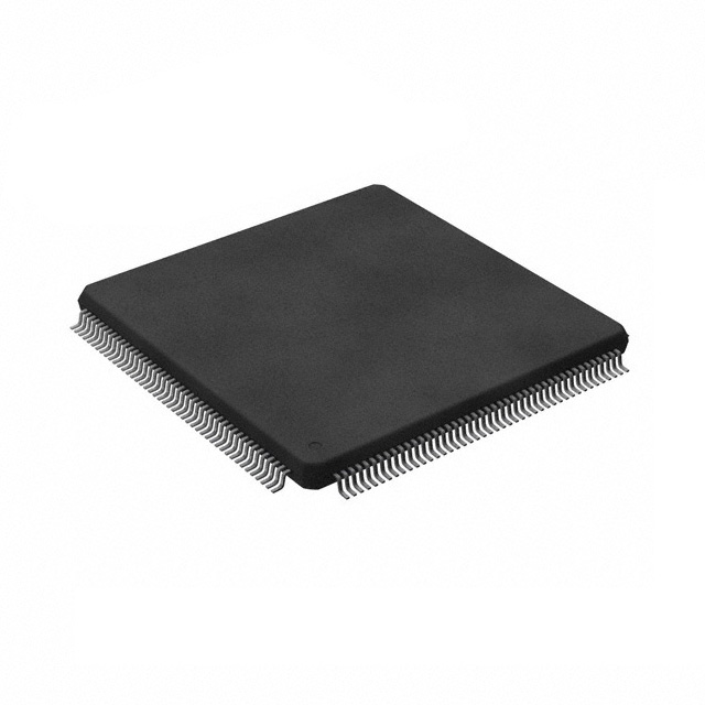


 工商网监
湘ICP备2023018690号
工商网监
湘ICP备2023018690号
