XRT86L30
SINGLE T1/E1/J1 FRAMER/LIU COMBO
JANUARY 2008
REV. 1.0.1
GENERAL DESCRIPTION
The XRT86L30 is a single channel 1.544 Mbit/s or
2.048 Mbit/s DS1/E1/J1 framer and LIU integrated
solution featuring R3 technology (Relayless,
Reconfigurable, Redundancy).
The physical
interface is optimized with internal impedance, and
with the patented pad structure, the XRT86L30
provides protection from power failures and hot
swapping.
The XRT86L30 contains an integrated DS1/E1/J1
framer and LIU which provide DS1/E1/J1 framing and
error accumulation in accordance with ANSI/ITU_T
specifications. The framer has a framing synchronizer
and transmit-receive slip buffers. The slip buffers can
be independently enabled or disabled as required
and can be configured to frame to the common DS1/
E1/J1 signal formats.
The Framer block contains a Transmit and Receive
T1/E1/J1 Framing function. There are 3 Transmit
HDLC controllers which encapsulate contents of the
Transmit HDLC buffers into LAPD Message frames.
There are 3 Receive HDLC controllers which extract
the payload content of Receive LAPD Message
frames from the incoming T1/E1/J1 data stream and
write the contents into the Receive HDLC buffers.
The framer also contains a Transmit and Overhead
Data Input port, which permits Data Link Terminal
Equipment direct access to the outbound T1/E1/J1
frames. Likewise, a Receive Overhead output data
port permits Data Link Terminal Equipment direct
access to the Data Link bits of the inbound T1/E1/J1
frames.
The XRT86L30 fully meets all of the latest T1/E1/J1
specifications:
ANSI T1/E1.107-1988, ANSI T1/
E1.403-1999, ANSI T1/E1.231-1993, ANSI T1/
E1.408-1990, AT&T TR 62411 (12-90) TR54016, and
ITU G-703, G.704, G706 and G.733, AT&T Pub.
43801, and ETS 300 011, 300 233, JT G.703, JT
G.704, JT G706, I.431. Extensive test and diagnostic
functions include Loop-backs, Boundary scan,
Pseudo Random bit sequence (PRBS) test pattern
generation, Performance Monitor, Bit Error Rate
(BER) meter, forced error insertion, and LAPD
unchannelized data payload processing according to
ITU-T standard Q.921.
Applications and Features (next page)
FIGURE 1. XRT86L30 1-CHANNEL DS1 (T1/E1/J1) FRAMER/LIU COMBO
Local PCM
Highway
External Data
Link Controller
XRT86L30
Tx Overhead In
Rx Overhead Out
1:2 Turns Ratio
Tx Serial
Data In
TTIP
2-Frame
Slip Buffer
Elastic Store
Tx Framer
ST-BUS
Tx Serial
Clock
Rx Serial
Clock
Tx LIU
Interface
LLB
TRING
LB
RTIP
Rx Serial
Data Out
2-Frame
Slip Buffer
Elastic Store
Rx Framer
Rx LIU
Interface
PRBS
Generator &
Analyser
Performance
Monitor
HDLC/LAPD
Controllers
LIU &
Loopback
Control
RRING
RxLOS
Line Side
8kHz sync
OSC
Back Plane
1.544-16.384 Mbit/s
1:1 Turns Ratio
Signaling &
Alarms
DMA
Interface
JTAG
Microprocessor
Interface
3
System (Terminal) Side
INT
TxON
Memory
D[7:0]
µP
A[11:0]
Select
4 WR
ALE_AS
RD
RDY_DTACK
Intel/Motorola µP
Configuration, Control &
Status Monitor
Exar Corporation 48720 Kato Road, Fremont CA, 94538 • (510) 668-7000 • FAX (510) 668-7017 • www.exar.com
�XRT86L30
SINGLE T1/E1/J1 FRAMER/LIU COMBO
REV. 1.0.1
APPLICATIONS
• High-Density T1/E1/J1 interfaces for Multiplexers, Switches, LAN Routers and Digital Modems
• SONET/SDH terminal or Add/Drop multiplexers (ADMs)
• T1/E1/J1 add/drop multiplexers (MUX)
• Channel Service Units (CSUs): T1/E1/J1 and Fractional T1/E1/J1
• Digital Access Cross-connect System (DACs)
• Digital Cross-connect Systems (DCS)
• Frame Relay Switches and Access Devices (FRADS)
• ISDN Primary Rate Interfaces (PRA)
• PBXs and PCM channel bank
• T3 channelized access concentrators and M13 MUX
• Wireless base stations
• ATM equipment with integrated DS1 interfaces
• Multichannel DS1 Test Equipment
• T1/E1/J1 Performance Monitoring
• Voice over packet gateways
• Routers
FEATURES
• Full duplex DS1 Tx and Rx Framer/LIU
• Two 512-bit (two-frame) elastic store, PCM frame slip buffers (FIFO) on TX and Rx provide up to 8.192 MHz
asynchronous back plane connections with jitter and wander attenuation
• Supports input PCM and signaling data at 1.544, 2.048, 4.096 and 8.192 Mbits. Also supports 4-channel
multiplexed 12.352/16.384 (HMVIP/H.100) Mbit/s on the back plane bus (with stuffed don’t care bits for the
other 3 channels)
• Programmable output clocks for Fractional T1/E1/J1
• Supports Channel Associated Signaling (CAS)
• Supports Common Channel Signalling (CCS)
• Supports ISDN Primary Rate Interface (ISDN PRI) signaling
• Extracts and inserts robbed bit signaling (RBS)
• 3 Integrated HDLC controllers for transmit and receive, each controller having two 96-byte buffers (buffer 0 /
buffer 1)
• HDLC Controllers Support SS7
• Timeslot assignable HDLC
• V5.1 or V5.2 Interface
• Automatic Performance Report Generation (PMON Status) can be inserted into the transmit LAPD interface
every 1 second or for a single transmission
• Alarm Indication Signal with Customer Installation signature (AIS-CI)
• Remote Alarm Indication with Customer Installation (RAI-CI)
• Gapped Clock interface mode for Transmit and Receive.
• Intel/Motorola and Power PC interfaces for configuration, control and status monitoring
• Parallel search algorithm for fast frame synchronization
• Wide choice of T1 framing structures: SF/D4, ESF, SLC®96, T1DM and N-Frame (non-signaling)
2
�XRT86L30
SINGLE T1/E1/J1 FRAMER/LIU COMBO
REV. 1.0.1
• Direct access to D and E channels for fast transmission of data link information
• PRBS, QRSS, and Network Loop Code generation and detection
• Programmable Interrupt output pin
• Supports programmed I/O and DMA modes of Read-Write access
• Each framer block encodes and decodes the T1/E1/J1 Frame serial data
• Detects and forces Red (SAI), Yellow (RAI) and Blue (AIS) Alarms
• Detects OOF, LOF, LOS errors and COFA conditions
• Loopbacks: Local (LLB) and Line remote (LB)
• Facilitates Inverse Multiplexing for ATM
• Performance monitor with one second polling
• Boundary scan (IEEE 1149.1) JTAG test port
• Accepts external 8kHz Sync reference
• 3.3V CMOS operation with 5V tolerant inputs
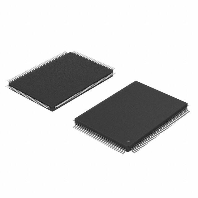
• 128-pin LQFP package with -40°C to +85°C operation
ORDERING INFORMATION
PART NUMBER
PACKAGE
OPERATING TEMPERATURE RANGE
XRT86L30IV
128 LQFP
-40°C to +85°C
3
�XRT86L30
SINGLE T1/E1/J1 FRAMER/LIU COMBO
REV. 1.0.1
LIST OF PARAGRAPHS
1.0 PIN LIST ...................................................................................................................................................4
2.0 PIN DESCRIPTIONS ................................................................................................................................8
3.0 MICROPROCESSOR INTERFACE BLOCK ..........................................................................................21
3.0.1 THE MICROPROCESSOR INTERFACE BLOCK SIGNALS ....................................................................................... 21
3.1 INTEL MODE PROGRAMMED I/O ACCESS (ASYNCHRONOUS) .................................................................. 24
3.2 MOTOROLA MODE PROGRAMMED I/O ACCESS (SYNCHRONOUS) .......................................................... 26
3.2.1 DMA READ/WRITE OPERATIONS .............................................................................................................................. 28
3.3 MEMORY MAPPED I/O ADDRESSING ............................................................................................................ 30
3.4 DESCRIPTION OF THE CONTROL REGISTERS ............................................................................................ 31
3.4.1 REGISTER DESCRIPTIONS ......................................................................................................................................... 37
3.5 PROGRAMMING THE LINE INTERFACE UNIT (LIU SECTION) ................................................................... 118
3.6 THE INTERRUPT STRUCTURE WITHIN THE FRAMER ............................................................................... 138
3.6.1 CONFIGURING THE INTERRUPT SYSTEM, AT THE FRAMER LEVEL .................................................................. 141
4.0 GENERAL DESCRIPTION AND INTERFACE .....................................................................................144
4.1 PHYSICAL INTERFACE .................................................................................................................................. 144
4.2 R3 TECHNOLOGY (RELAYLESS / RECONFIGURABLE / REDUNDANCY) ................................................ 145
4.2.1 LINE CARD REDUNDANCY ....................................................................................................................................... 145
4.2.2 TYPICAL REDUNDANCY SCHEMES ........................................................................................................................ 145
4.2.3 1:1 AND 1+1 REDUNDANCY WITHOUT RELAYS .................................................................................................... 145
4.2.4 TRANSMIT INTERFACE WITH 1:1 AND 1+1 REDUNDANCY .................................................................................. 145
4.2.5 RECEIVE INTERFACE WITH 1:1 AND 1+1 REDUNDANCY ..................................................................................... 146
4.3 POWER FAILURE PROTECTION ................................................................................................................... 147
4.4 OVERVOLTAGE AND OVERCURRENT PROTECTION ................................................................................ 147
4.5 NON-INTRUSIVE MONITORING ..................................................................................................................... 147
4.6 T1/E1 SERIAL PCM INTERFACE ................................................................................................................... 148
4.7 T1/E1 FRACTIONAL INTERFACE .................................................................................................................. 149
4.8 T1/E1 TIME SLOT SUBSTITUTION AND CONTROL ..................................................................................... 150
4.9 ROBBED BIT SIGNALING/CAS SIGNALING ................................................................................................. 151
4.10 OVERHEAD INTERFACE .............................................................................................................................. 153
4.11 FRAMER BYPASS MODE ............................................................................................................................. 154
4.12 HIGH-SPEED NON-MULTIPLEXED INTERFACE ........................................................................................ 155
4.13 HIGH-SPEED MULTIPLEXED INTERFACE ................................................................................................. 156
5.0 LOOPBACK MODES OF OPERATION ...............................................................................................157
5.1 LIU PHYSICAL INTERFACE LOOPBACK DIAGNOSTICS ............................................................................ 157
5.1.1 LOCAL ANALOG LOOPBACK .................................................................................................................................. 157
5.1.2 REMOTE LOOPBACK ................................................................................................................................................ 157
5.1.3 DIGITAL LOOPBACK ................................................................................................................................................. 158
5.1.4 DUAL LOOPBACK ..................................................................................................................................................... 158
5.1.5 FRAMER REMOTE LINE LOOPBACK ...................................................................................................................... 158
5.1.6 FRAMER PAYLOAD LOOPBACK ............................................................................................................................. 159
5.1.7 FRAMER LOCAL LOOPBACK ................................................................................................................................... 159
6.0 HDLC CONTROLLERS AND LAPD MESSAGES ...............................................................................160
6.1 PROGRAMMING SEQUENCE FOR SENDING LESS THAN 96-BYTE MESSAGES .................................... 160
6.2 PROGRAMMING SEQUENCE FOR SENDING LARGE MESSAGES ........................................................... 160
6.3 PROGRAMMING SEQUENCE FOR RECEIVING LAPD MESSAGES ........................................................... 161
6.4 SS7 (SIGNALING SYSTEM NUMBER 7) FOR ESF IN DS1 ONLY ................................................................ 161
6.5 DS1/E1 DATALINK TRANSMISSION USING THE HDLC CONTROLLERS ................................................. 162
6.6 TRANSMIT BOS (BIT ORIENTED SIGNALING) PROCESSOR ..................................................................... 162
6.6.1 DESCRIPTION OF BOS .............................................................................................................................................. 162
6.6.2 PRIORITY CODEWORD MESSAGE .......................................................................................................................... 162
6.6.3 COMMAND AND RESPONSE INFORMATION .......................................................................................................... 162
6.7 TRANSMIT MOS (MESSAGE ORIENTED SIGNALING) PROCESSOR ........................................................ 163
6.7.1 DISCUSSION OF MOS ............................................................................................................................................... 163
6.7.2 PERIODIC PERFORMANCE REPORT ...................................................................................................................... 163
6.7.3 TRANSMISSION-ERROR EVENT .............................................................................................................................. 164
6.7.4 PATH AND TEST SIGNAL IDENTIFICATION MESSAGE ......................................................................................... 164
6.7.5 FRAME STRUCTURE ................................................................................................................................................. 164
6.7.6 FLAG SEQUENCE ...................................................................................................................................................... 164
6.7.7 ADDRESS FIELD ........................................................................................................................................................ 165
6.7.8 ADDRESS FIELD EXTENSION BIT (EA) ................................................................................................................... 165
I
�XRT86L30
REV. 1.0.1
SINGLE T1/E1/J1 FRAMER/LIU COMBO
6.7.9 COMMAND OR RESPONSE BIT (C/R) ...................................................................................................................... 165
6.7.10 SERVICE ACCESS POINT IDENTIFIER (SAPI) ...................................................................................................... 165
6.7.11 TERMINAL ENDPOINT IDENTIFIER (TEI) ............................................................................................................... 165
6.7.12 CONTROL FIELD ...................................................................................................................................................... 165
6.7.13 FRAME CHECK SEQUENCE (FCS) FIELD ............................................................................................................. 165
6.7.14 TRANSPARENCY (ZERO STUFFING) ..................................................................................................................... 166
6.8 TRANSMIT SLC®96 DATA LINK CONTROLLER .......................................................................................... 167
6.9 D/E TIME SLOT TRANSMIT HDLC CONTROLLER BLOCK V5.1 OR V5.2 INTERFACE ............................ 168
6.10 AUTOMATIC PERFORMANCE REPORT (APR) .......................................................................................... 168
6.10.1 BIT VALUE INTERPRETATION ............................................................................................................................... 168
7.0 OVERHEAD INTERFACE BLOCK ...................................................................................................... 170
7.1 DS1 TRANSMIT OVERHEAD INPUT INTERFACE BLOCK .......................................................................... 170
7.1.1 DESCRIPTION OF THE DS1 TRANSMIT OVERHEAD INPUT INTERFACE BLOCK .............................................. 170
7.1.2 CONFIGURE THE DS1 TRANSMIT OVERHEAD INPUT INTERFACE MODULE AS SOURCE OF THE FACILITY DATA
LINK (FDL) BITS IN ESF FRAMING FORMAT MODE ............................................................................................... 170
7.1.3 CONFIGURE THE DS1 TRANSMIT OVERHEAD INPUT INTERFACE MODULE AS SOURCE OF THE SIGNALING
FRAMING (FS) BITS IN N OR SLC®96 FRAMING FORMAT MODE ........................................................................ 172
7.1.4 CONFIGURE THE DS1 TRANSMIT OVERHEAD INPUT INTERFACE MODULE AS SOURCE OF THE REMOTE SIGNALING (R) BITS IN T1DM FRAMING FORMAT MODE ........................................................................................... 173
7.2 DS1 RECEIVE OVERHEAD OUTPUT INTERFACE BLOCK ......................................................................... 173
7.2.1 DESCRIPTION OF THE DS1 RECEIVE OVERHEAD OUTPUT INTERFACE BLOCK ............................................. 174
7.2.2 CONFIGURE THE DS1 RECEIVE OVERHEAD OUTPUT INTERFACE MODULE AS DESTINATION OF THE FACILITY
DATA LINK (FDL) BITS IN ESF FRAMING FORMAT MODE .................................................................................... 174
7.2.3 CONFIGURE THE DS1 RECEIVE OVERHEAD OUTPUT INTERFACE MODULE AS DESTINATION OF THE SIGNALING
FRAMING (FS) BITS IN N OR SLC®96 FRAMING FORMAT MODE ........................................................................ 175
7.2.4 CONFIGURE THE DS1 RECEIVE OVERHEAD OUTPUT INTERFACE MODULE AS DESTINATION OF THE REMOTE
SIGNALING (R) BITS IN T1DM FRAMING FORMAT MODE ..................................................................................... 176
7.3 E1 OVERHEAD INTERFACE BLOCK ............................................................................................................ 177
7.4 E1 TRANSMIT OVERHEAD INPUT INTERFACE BLOCK ............................................................................. 177
7.4.1 DESCRIPTION OF THE E1 TRANSMIT OVERHEAD INPUT INTERFACE BLOCK ................................................. 177
7.4.2 CONFIGURE THE E1 TRANSMIT OVERHEAD INPUT INTERFACE MODULE AS SOURCE OF THE NATIONAL BIT SEQUENCE IN E1 FRAMING FORMAT MODE .............................................................................................................. 178
7.5 E1 RECEIVE OVERHEAD INTERFACE ......................................................................................................... 180
7.5.1 DESCRIPTION OF THE E1 RECEIVE OVERHEAD OUTPUT INTERFACE BLOCK ............................................... 180
7.5.2 CONFIGURE THE E1 RECEIVE OVERHEAD OUTPUT INTERFACE MODULE AS SOURCE OF THE NATIONAL BIT
SEQUENCE IN E1 FRAMING FORMAT MODE .......................................................................................................... 181
8.0 LIU TRANSMIT PATH ......................................................................................................................... 183
8.1 TRANSMIT DIAGNOSTIC FEATURES ........................................................................................................... 183
8.1.1 TAOS (TRANSMIT ALL ONES) .................................................................................................................................. 183
8.1.2 ATAOS (AUTOMATIC TRANSMIT ALL ONES) ......................................................................................................... 184
8.1.3 NETWORK LOOP UP CODE ...................................................................................................................................... 184
8.1.4 NETWORK LOOP DOWN CODE ............................................................................................................................... 184
8.1.5 QRSS GENERATION .................................................................................................................................................. 185
8.2 T1 LONG HAUL LINE BUILD OUT (LBO) ...................................................................................................... 185
8.3 T1 SHORT HAUL LINE BUILD OUT (LBO) .................................................................................................... 186
8.3.1 ARBITRARY PULSE GENERATOR ........................................................................................................................... 186
8.3.2 DMO (DIGITAL MONITOR OUTPUT) ......................................................................................................................... 187
8.3.3 TRANSMIT JITTER ATTENUATOR ........................................................................................................................... 187
8.4 LINE TERMINATION (TTIP/TRING) ................................................................................................................ 188
9.0 LIU RECEIVE PATH ............................................................................................................................ 189
9.1 LINE TERMINATION (RTIP/RRING) ............................................................................................................... 189
9.1.1 CASE 1: INTERNAL TERMINATION .......................................................................................................................... 189
9.1.2 CASE 2: INTERNAL TERMINATION WITH ONE EXTERNAL FIXED RESISTOR FOR ALL MODES .................... 189
9.1.3 EQUALIZER CONTROL ............................................................................................................................................. 190
9.1.4 CABLE LOSS INDICATOR ......................................................................................................................................... 190
9.2 RECEIVE SENSITIVITY ................................................................................................................................... 191
9.2.1 AIS (ALARM INDICATION SIGNAL) .......................................................................................................................... 191
9.2.2 NLCD (NETWORK LOOP CODE DETECTION) ......................................................................................................... 191
9.2.3 FLSD (FIFO LIMIT STATUS DETECTION) ................................................................................................................ 192
9.2.4 RECEIVE JITTER ATTENUATOR .............................................................................................................................. 192
9.2.5 RXMUTE (RECEIVER LOS WITH DATA MUTING) ................................................................................................... 192
10.0 THE E1 TRANSMIT/RECEIVE FRAMER .......................................................................................... 194
10.1 DESCRIPTION OF THE TRANSMIT/RECEIVE PAYLOAD DATA INPUT INTERFACE BLOCK ................ 194
10.1.1 BRIEF DISCUSSION OF THE TRANSMIT/RECEIVE PAYLOAD DATA INPUT INTERFACE BLOCK OPERATING AT
II
�XRT86L30
SINGLE T1/E1/J1 FRAMER/LIU COMBO
REV. 1.0.1
XRT84V24 COMPATIBLE 2.048MBIT/S MODE .......................................................................................................... 194
10.2 TRANSMIT/RECEIVE HIGH-SPEED BACK-PLANE INTERFACE ............................................................... 197
10.2.1 NON-MULTIPLEXED HIGH-SPEED MODE ............................................................................................................. 197
10.2.2 MULTIPLEXED HIGH-SPEED MODE ...................................................................................................................... 200
10.3 BRIEF DISCUSSION OF COMMON CHANNEL SIGNALING IN E1 FRAMING FORMAT .......................... 206
10.4 BRIEF DISCUSSION OF CHANNEL ASSOCIATED SIGNALING IN E1 FRAMING FORMAT ................... 206
10.5 INSERT/EXTRACT SIGNALING BITS FROM TSCR REGISTER ................................................................. 206
10.6 INSERT/EXTRACT SIGNALING BITS FROM TXCHN[0]_N/TXSIG PIN ...................................................... 206
10.7 ENABLE CHANNEL ASSOCIATED SIGNALING AND SIGNALING DATA SOURCE CONTROL ............. 207
11.0 THE DS1 TRANSMIT/RECEIVE FRAMER ........................................................................................208
11.1 DESCRIPTION OF THE TRANSMIT/RECEIVE PAYLOAD DATA INPUT INTERFACE BLOCK ................ 208
11.1.1 BRIEF DISCUSSION OF THE TRANSMIT/RECEIVE PAYLOAD DATA INPUT INTERFACE BLOCK OPERATING AT
1.544MBIT/S MODE ..................................................................................................................................................... 208
11.2 TRANSMIT/RECEIVE HIGH-SPEED BACK-PLANE INTERFACE ............................................................... 211
11.2.1 T1 TRANSMIT/RECEIVE INTERFACE - MVIP 2.048 MHZ ...................................................................................... 211
11.2.2 NON-MULTIPLEXED HIGH-SPEED MODE ............................................................................................................. 212
11.2.3 MULTIPLEXED HIGH-SPEED MODE ...................................................................................................................... 214
11.3 BRIEF DISCUSSION OF ROBBED-BIT SIGNALING IN DS1 FRAMING FORMAT .................................... 220
11.3.1 CONFIGURE THE FRAMER TO TRANSMIT ROBBED-BIT SIGNALING ............................................................... 220
11.3.2 INSERT SIGNALING BITS FROM TSCR REGISTER .............................................................................................. 221
11.3.3 INSERT SIGNALING BITS FROM TXSIG_N PIN ..................................................................................................... 221
12.0 ALARMS AND ERROR CONDITIONS ..............................................................................................223
12.1 AIS ALARM .................................................................................................................................................... 223
12.2 RED ALARM .................................................................................................................................................. 225
12.3 YELLOW ALARM .......................................................................................................................................... 226
12.4 BIPOLAR VIOLATION ................................................................................................................................... 228
12.5 E1 BRIEF DISCUSSION OF ALARMS AND ERROR CONDITIONS ........................................................... 231
12.5.1 HOW TO CONFIGURE THE FRAMER TO TRANSMIT AIS .................................................................................... 236
12.5.2 HOW TO CONFIGURE THE FRAMER TO GENERATE RED ALARM ................................................................... 237
12.5.3 HOW TO CONFIGURE THE FRAMER TO TRANSMIT YELLOW ALARM ............................................................. 237
12.5.4 TRANSMIT YELLOW ALARM .................................................................................................................................. 238
12.5.5 TRANSMIT CAS MULTI-FRAME YELLOW ALARM ............................................................................................... 238
12.6 T1 BRIEF DISCUSSION OF ALARMS AND ERROR CONDITIONS ............................................................ 239
12.6.1 HOW TO CONFIGURE THE FRAMER TO TRANSMIT AIS .................................................................................... 242
12.6.2 HOW TO CONFIGURE THE FRAMER TO GENERATE RED ALARM ................................................................... 243
12.6.3 HOW TO CONFIGURE THE FRAMER TO TRANSMIT YELLOW ALARM ............................................................. 243
12.6.4 TRANSMIT YELLOW ALARM IN SF MODE ............................................................................................................ 244
12.6.5 TRANSMIT YELLOW ALARM IN ESF MODE .......................................................................................................... 244
12.6.6 TRANSMIT YELLOW ALARM IN N MODE .............................................................................................................. 244
12.6.7 TRANSMIT YELLOW ALARM IN T1DM MODE ....................................................................................................... 244
13.0 PERFORMANCE MONITORING (PMON) .........................................................................................247
13.1 RECEIVE LINE CODE VIOLATION COUNTER (16-BIT) .............................................................................. 247
13.2 16-BIT RECEIVE FRAME ALIGNMENT ERROR COUNTER (16-BIT) ......................................................... 247
13.3 RECEIVE SEVERELY ERRORED FRAME COUNTER (8-BIT) .................................................................... 247
13.4 RECEIVE CRC-6/4 BLOCK ERROR COUNTER (16-BIT) ............................................................................ 247
13.5 RECEIVE FAR-END BLOCK ERROR COUNTER (16-BIT) .......................................................................... 247
13.6 RECEIVE SLIP COUNTER (8-BIT) ................................................................................................................ 247
13.7 RECEIVE LOSS OF FRAME COUNTER (8-BIT) .......................................................................................... 247
13.8 RECEIVE CHANGE OF FRAME ALIGNMENT COUNTER (8-BIT) .............................................................. 247
13.9 FRAME CHECK SEQUENCE ERROR COUNTERS 1, 2, AND 3 (8-BIT EACH) ......................................... 247
13.10 PRBS ERROR COUNTER (16-BIT) ............................................................................................................. 247
13.11 TRANSMIT SLIP COUNTER (8-BIT) ........................................................................................................... 247
13.12 EXCESSIVE ZERO VIOLATION COUNTER (16-BIT) ................................................................................. 248
14.0 APPENDIX A: DS-1/E1 FRAMING FORMATS ..................................................................................249
14.1 THE E1 FRAMING STRUCTURE .................................................................................................................. 249
14.1.1 FAS FRAME .............................................................................................................................................................. 249
14.1.2 NON-FAS FRAME ..................................................................................................................................................... 250
14.2 THE E1 MULTI-FRAME STRUCTURE .......................................................................................................... 251
14.2.1 THE CRC MULTI-FRAME STRUCTURE .................................................................................................................. 251
14.2.2 CAS MULTI-FRAMES AND CHANNEL ASSOCIATED SIGNALING ...................................................................... 253
14.3 THE DS1 FRAMING STRUCTURE ................................................................................................................ 255
14.4 T1 SUPER FRAME FORMAT (SF) ................................................................................................................ 256
III
�XRT86L30
REV. 1.0.1
SINGLE T1/E1/J1 FRAMER/LIU COMBO
14.5 T1 EXTENDED SUPERFRAME FORMAT (ESF) .......................................................................................... 258
14.6 T1 NON-SIGNALING FRAME FORMAT ....................................................................................................... 260
14.7 T1 DATA MULTIPLEXED FRAMING FORMAT (T1DM) ............................................................................... 260
14.8 SLC-96 FORMAT (SLC-96) ........................................................................................................................... 261
IV
�XRT86L30
SINGLE T1/E1/J1 FRAMER/LIU COMBO
REV. 1.0.1
LIST OF FIGURES
Figure 1.: XRT86L30 1-channel DS1 (T1/E1/J1) Framer/LIU Combo ............................................................................... 1
Figure 2.: Simplified Block Diagram of the Microprocessor Interface Block .................................................................... 21
Figure 3.: Intel µP Interface Signals During Programmed I/O Read and Write Operations ............................................. 25
Figure 4.: Motorola µP Interface Signals During Programmed I/O Read and Write Operations ...................................... 27
Figure 5.: Motorola 68K µP Interface Signals During Programmed I/O Read and Write Operations .............................. 28
Figure 6.: DMA Mode for the XRT86L30 and a Microprocessor ...................................................................................... 29
Figure 7.: LIU Transmit Connection Diagram Using Internal Termination ..................................................................... 144
Figure 8.: LIU Receive Connection Diagram Using Internal Termination ..................................................................... 144
Figure 9.: Simplified Block Diagram of the Transmit Interface for 1:1 and 1+1 Redundancy ........................................ 145
Figure 10.: Simplified Block Diagram of the Receive Interface for 1:1 and 1+1 Redundancy ....................................... 146
Figure 11.: Simplified Block Diagram of a Non-Intrusive Monitoring Application ........................................................... 147
Figure 12.: Transmit T1/E1 Serial PCM Interface .......................................................................................................... 148
Figure 13.: Receive T1/E1 Serial PCM Interface ........................................................................................................... 148
Figure 14.: T1 Fractional Interface ................................................................................................................................. 149
Figure 15.: T1/E1 Time Slot Substitution and Control .................................................................................................... 150
Figure 16.: Robbed Bit Signaling / CAS Signaling ......................................................................................................... 151
Figure 17.: ESF / CAS External Signaling Bus .............................................................................................................. 151
Figure 18.: SF / SLC-96 or 4-code Signaling in ESF / CAS External Signaling Bus ...................................................... 152
Figure 19.: T1/E1 Overhead Interface ........................................................................................................................... 153
Figure 20.: T1 External Overhead Datalink Bus ............................................................................................................ 153
Figure 21.: E1 Overhead External Datalink Bus ............................................................................................................ 154
Figure 22.: Simplified Block Diagram of the Framer Bypass Mode ............................................................................... 154
Figure 23.: T1 High-Speed Non-Multiplexed Interface ................................................................................................... 155
Figure 24.: E1 High-Speed Non-Multiplexed Interface .................................................................................................. 155
Figure 25.: Transmit High-Speed Bit Multiplexed Block Diagram .................................................................................. 156
Figure 26.: Receive High-Speed Bit Multiplexed Block Diagram ................................................................................... 156
Figure 27.: Simplified Block Diagram of Local Analog Loopback .................................................................................. 157
Figure 28.: Simplified Block Diagram of Remote Loopback ........................................................................................... 157
Figure 29.: Simplified Block Diagram of Digital Loopback ............................................................................................. 158
Figure 30.: Simplified Block Diagram of Dual Loopback ................................................................................................ 158
Figure 31.: Simplified Block Diagram of the Framer Remote Line Loopback ................................................................ 158
Figure 32.: Simplified Block Diagram of the Framer Local Loopback ............................................................................ 159
Figure 33.: Simplified Block Diagram of the Framer Local Loopback ............................................................................ 159
Figure 34.: HDLC Controllers ......................................................................................................................................... 160
Figure 35.: LAPD Frame Structure ................................................................................................................................ 163
Figure 36.: Block Diagram of the DS1 Transmit Overhead Input Interface of the XRT86L30 ....................................... 170
Figure 37.: DS1 Transmit Overhead Input Interface Timing in ESF Framing Format mode .......................................... 172
Figure 38.: DS1 Transmit Overhead Input Timing in N or SLC®96 Framing Format Mode .......................................... 173
Figure 39.: DS1 Transmit Overhead Input Interface module in T1DM Framing Format mode ...................................... 173
Figure 40.: Block Diagram of the DS1 Receive Overhead Output Interface of XRT86L30 ............................................ 174
Figure 41.: DS1 Receive Overhead Output Interface module in ESF framing format mode ......................................... 175
Figure 42.: DS1 Receive Overhead Output Interface Timing in N or SLC®96 Framing Format mode .......................... 176
Figure 43.: DS1 Receive Overhead Output Interface Timing in T1DM Framing Format mode ..................................... 177
Figure 44.: Block Diagram of the E1 Transmit Overhead Input Interface of XRT86L30 ................................................ 178
Figure 45.: E1 Transmit Overhead Input Interface Timing ............................................................................................. 180
Figure 46.: Block Diagram of the E1 Receive Overhead Output Interface of XRT86L30 .............................................. 180
Figure 47.: E1 Receive Overhead Output Interface Timing ........................................................................................... 182
Figure 48.: TAOS (Transmit All Ones) ........................................................................................................................... 183
Figure 49.: Simplified Block Diagram of the ATAOS Function ....................................................................................... 184
Figure 50.: Network Loop Up Code Generation ............................................................................................................. 184
Figure 51.: Network Loop Down Code Generation ........................................................................................................ 184
Figure 52.: Long Haul Line Build Out with -7.5dB Attenuation ....................................................................................... 185
Figure 53.: Long Haul Line Build Out with -15dB Attenuation ........................................................................................ 185
Figure 54.: Long Haul Line Build Out with -22.5dB Attenuation ..................................................................................... 186
Figure 55.: Arbitrary Pulse Segment Assignment .......................................................................................................... 187
Figure 56.: Typical Connection Diagram Using Internal Termination ............................................................................ 188
Figure 57.: Typical Connection Diagram Using Internal Termination ........................................................................... 189
Figure 58.: Typical Connection Diagram Using One External Fixed Resistor ............................................................... 190
V
�XRT86L30
REV. 1.0.1
SINGLE T1/E1/J1 FRAMER/LIU COMBO
Figure 59.: Simplified Block Diagram of the Equalizer and Peak Detector .................................................................... 190
Figure 60.: Simplified Block Diagram of the Cable Loss Indicator ................................................................................. 190
Figure 61.: Test Configuration for Measuring Receive Sensitivity ................................................................................. 191
Figure 62.: Process Block for Automatic Loop Code Detection ..................................................................................... 192
Figure 63.: Simplified Block Diagram of the RxMUTE Function .................................................................................... 193
Figure 64.: Interfacing the Transmit Path to local terminal equipment .......................................................................... 194
Figure 66.: Waveforms for connecting the Transmit Payload Data Input Interface Block to local Terminal Equipment 195
Figure 65.: Interfacing the Receive Path to local terminal equipment ........................................................................... 195
Figure 67.: Waveforms for connecting the Receive Payload Data Input Interface Block to local Terminal Equipment . 196
Figure 68.: Transmit Non-Multiplexed High-Speed Connection to local terminal equipment using MVIP 2.048Mbit/s,
4.096Mbit/s, or 8.192Mbit/s ............................................................................................................................. 197
Figure 70.: Waveforms for Connecting the Transmit Non-Multiplexed High-Speed Input Interface at MVIP 2.048Mbit/s,
4.096Mbit/s, and 8.192Mbit/s .......................................................................................................................... 198
Figure 69.: Receive Non-Multiplexed High-Speed Connection to local terminal equipment using MVIP 2.048Mbit/s,
4.096Mbit/s, or 8.192Mbit/s ............................................................................................................................. 198
Figure 71.: Waveforms for Connecting the Receive Non-Multiplexed High-Speed Input Interface at MVIP 2.048Mbit/s,
4.096Mbit/s, and 8.192Mbit/s .......................................................................................................................... 199
Figure 72.: Interfacing XRT86L30 Transmit to local terminal equipment using 16.384Mbit/s, HMVIP 16.384Mbit/s, and H.100
16.384Mbit/s .................................................................................................................................................... 202
Figure 73.: Interfacing XRT86L30 Receive to local terminal equipment using 16.384Mbit/s, HMVIP 16.384Mbit/s, and H.100
16.384Mbit/s .................................................................................................................................................... 203
Figure 74.: Waveforms for Connecting the Transmit Multiplexed High-Speed Input Interface at HMVIP And H.100
16.384Mbit/s mode .......................................................................................................................................... 204
Figure 75.: Waveforms for Connecting the Receive Multiplexed High-Speed Input Interface at HMVIP 16.384Mbit/s mode
204
Figure 76.: Waveforms for Connecting the Receive Multiplexed High-Speed Input Interface at H.100 16.384Mbit/s mode
205
Figure 77.: Timing Diagram of the TxSIG Input ............................................................................................................. 206
Figure 78.: Timing Diagram of the RxSIG Output .......................................................................................................... 207
Figure 79.: Interfacing the Transmit Path to local terminal equipment .......................................................................... 208
Figure 81.: Waveforms for connecting the Transmit Payload Data Input Interface Block to local Terminal Equipment 209
Figure 80.: Interfacing the Receive Path to local terminal equipment ........................................................................... 209
Figure 82.: Waveforms for connecting the Receive Payload Data Input Interface Block to local Terminal Equipment . 210
Figure 83.: Transmit Non-Multiplexed High-Speed Connection to local terminal equipment using MVIP 2.048Mbit/s,
4.096Mbit/s, or 8.192Mbit/s ............................................................................................................................. 212
Figure 84.: Receive Non-Multiplexed High-Speed Connection to local terminal equipment using MVIP 2.048Mbit/s,
4.096Mbit/s, or 8.192Mbit/s ............................................................................................................................. 212
Figure 85.: Waveforms for Connecting the Transmit Non-Multiplexed High-Speed Input Interface at MVIP 2.048Mbit/s,
4.096Mbit/s, and 8.192Mbit/s .......................................................................................................................... 213
Figure 86.: Waveforms for Connecting the Receive Non-Multiplexed High-Speed Input Interface at MVIP 2.048Mbit/s,
4.096Mbit/s, and 8.192Mbit/s .......................................................................................................................... 213
Figure 87.: Interfacing XRT86L30 Transmit to local terminal equipment using 16.384Mbit/s, HMVIP 16.384Mbit/s, and H.100
16.384Mbit/s .................................................................................................................................................... 216
Figure 88.: Interfacing XRT86L30 Receive to local terminal equipment using 16.384Mbit/s, HMVIP 16.384Mbit/s, and H.100
16.384Mbit/s .................................................................................................................................................... 217
Figure 89.: Waveforms for Connecting the Transmit Multiplexed High-Speed Input Interface at 12.352Mbit/s mode .. 217
Figure 91.: Waveforms for Connecting the Transmit Multiplexed High-Speed Input Interface at HMVIP and H.100
16.384Mbit/s mode .......................................................................................................................................... 218
Figure 92.: Waveforms for Connecting the Receive Multiplexed High-Speed Input Interface at 12.352Mbit/s mode ... 218
Figure 90.: Waveforms for Connecting the Transmit Multiplexed High-Speed Input Interface at 16.384Mbit/s mode .. 218
Figure 95.: Waveforms for Connecting the Receive Multiplexed High-Speed Input Interface at H.100 16.384Mbit/s mode
219
Figure 93.: Waveforms for Connecting the Receive Multiplexed High-Speed Input Interface at 16.384Mbit/s mode ... 219
Figure 94.: Waveforms for Connecting the Receive Multiplexed High-Speed Input Interface at HMVIP 16.384Mbit/s mode
219
Figure 96.: Timing Diagram of the TxSig_n Input .......................................................................................................... 222
Figure 97.: Simple Diagram of E1 system model .......................................................................................................... 231
Figure 98.: Generation of Yellow Alarm by the Repeater upon detection of line failure ................................................ 232
Figure 99.: Generation of AIS by the Repeater upon detection of line failure ............................................................... 233
Figure 100.: Generation of Yellow Alarm by the CPE upon detection of AIS originated by the Repeater ..................... 234
VI
�XRT86L30
SINGLE T1/E1/J1 FRAMER/LIU COMBO
REV. 1.0.1
Figure 101.: Generation of CAS Multi-frame Yellow Alarm and AIS16 by the Repeater ............................................... 235
Figure 102.: Generation of CAS Multi-frame Yellow Alarm by the CPE upon detection of “AIS16” pattern sent by the Repeater
236
Figure 103.: Simple Diagram of DS1 System Model ..................................................................................................... 239
Figure 104.: Generation of Yellow Alarm by the CPE upon detection of line failure ...................................................... 240
Figure 105.: Generation of AIS by the Repeater upon detection of Yellow Alarm originated by the CPE ..................... 241
Figure 106.: Generation of Yellow Alarm by the CPE upon detection of AIS originated by the Repeater ..................... 242
Figure 107.: Single E1 Frame Diagram ......................................................................................................................... 249
Figure 108.: Frame/Byte Format of the CAS Multi-Frame Structure .............................................................................. 253
Figure 109.: E1 Frame Format ....................................................................................................................................... 254
Figure 110.: T1 Frame Format ....................................................................................................................................... 255
Figure 111.: T1 Superframe PCM Format ..................................................................................................................... 256
Figure 112.: T1 Extended Superframe Format .............................................................................................................. 258
Figure 113.: T1DM Frame Format ................................................................................................................................. 260
Figure 114.: Framer System Transmit Timing Diagram ................................................................................................. 263
Figure 115.: Framer System Receive Timing Diagram (RxSERCLK as an Output) ...................................................... 264
Figure 116.: Framer System Receive Timing Diagram (RxSERCLK as an Input) ......................................................... 265
Figure 117.: Framer System Transmit Overhead Timing Diagram ................................................................................ 265
Figure 118.: Framer System Receive Overhead Timing Diagram (RxSERCLK as an Output) ..................................... 266
Figure 119.: Framer System Receive Overhead Timing Diagram (RxSERCLK as an Input) ........................................ 266
Figure 120.: ITU G.703 Pulse Template ........................................................................................................................ 270
Figure 121.: DSX-1 Pulse Template (normalized amplitude) ......................................................................................... 271
VII
�XRT86L30
REV. 1.0.1
SINGLE T1/E1/J1 FRAMER/LIU COMBO
LIST OF TABLES
Table 1:: List by Pin Number ............................................................................................................................................. 4
Table 2:: Selecting the Microprocessor Interface Mode .................................................................................................. 21
Table 3:: XRT86L30 Microprocessor Interface Signals that exhibit constant roles in both Intel and Motorola Modes .... 22
Table 4:: Intel mode: Microprocessor Interface Signals ................................................................................................... 22
Table 5:: Motorola Mode: Microprocessor Interface Signals ........................................................................................... 23
Table 6:: Intel Microprocessor Interface Timing Specifications ....................................................................................... 25
Table 7:: Intel Microprocessor Interface Timing Specifications ....................................................................................... 27
Table 8:: Motorola 68K Microprocessor Interface Timing Specifications ......................................................................... 28
Table 9:: XRT86L30 Framer/LIU Register Map ............................................................................................................... 30
Table 10:: Register Summary .......................................................................................................................................... 31
Table 11:: Clock Select Register E1 Mode ...................................................................................................................... 37
Table 12:: Line Interface Control Register T1 Mode ........................................................................................................ 38
Table 13:: General Purpose Input/Output 0 Control Register .......................................................................................... 38
Table 14:: Framing Select Register-E1 Mode .................................................................................................................. 39
Table 15:: Framing Select Register-T1 Mode .................................................................................................................. 40
Table 16:: Alarm Generation Register - E1 Mode ............................................................................................................ 41
Table 17:: Alarm Generation Register -T1 Mode ............................................................................................................. 42
Table 18:: Synchronization MUX Register - E1 Mode ..................................................................................................... 44
Table 19:: Synchronization MUX Register - T1 Mode ..................................................................................................... 45
Table 20:: Transmit Signaling and Data Link Select Register - E1 Mode ........................................................................ 46
Table 21:: Transmit Signaling and Data Link Select Register - T1 Mode ........................................................................ 47
Table 22:: Framing Control Register E1 Mode ................................................................................................................ 48
Table 23:: Framing Control Register T1 Mode ................................................................................................................ 49
Table 24:: Receive Signaling & Data Link Select Register - E1 Mode ............................................................................ 50
Table 25:: Receive Signaling & Data Link Select Register (RS&DLSR) T1 Mode .......................................................... 51
Table 26:: Signaling Change Register 0 - T1 Mode ......................................................................................................... 52
Table 27:: Signaling Change Register 1 .......................................................................................................................... 52
Table 28:: Signaling Change Register 2 .......................................................................................................................... 53
Table 29:: Signaling Change Register 3 .......................................................................................................................... 53
Table 30:: Receive National Bits Register ....................................................................................................................... 53
Table 31:: Receive Extra Bits Register ............................................................................................................................ 54
Table 32:: Data Link Control Register .............................................................................................................................. 55
Table 33:: Transmit Data Link Byte Count Register ........................................................................................................ 56
Table 34:: Receive Data Link Byte Count Register ......................................................................................................... 57
Table 35:: Slip Buffer Control Register ............................................................................................................................ 57
Table 36:: FIFO Latency Register .................................................................................................................................... 58
Table 37:: DMA 0 (Write) Configuration Register ............................................................................................................ 58
Table 38:: DMA 1 (Read) Configuration Register ............................................................................................................ 59
Table 39:: Interrupt Control Register ............................................................................................................................... 60
Table 40:: LAPD Select Register ..................................................................................................................................... 60
Table 41:: Customer Installation Alarm Generation Register .......................................................................................... 61
Table 42:: Performance Report Control Register ............................................................................................................ 61
Table 43:: Gapped Clock Control Register ...................................................................................................................... 62
Table 44:: Gapped Clock Control Register ...................................................................................................................... 62
Table 45:: Transmit Interface Control Register - E1 Mode .............................................................................................. 63
Table 46:: Transmit Interface Control Register - T1 Mode .............................................................................................. 64
Table 47:: Receive Interface Control Register (RICR) - E1 Mode ................................................................................... 66
Table 48:: Receive Interface Control Register (RICR) - T1 Mode ................................................................................... 67
Table 49:: DS1 Test Register .......................................................................................................................................... 68
Table 50:: Loopback Code Control Register .................................................................................................................... 69
Table 51:: Transmit Loopback Coder Register ................................................................................................................ 70
Table 52:: Receive Loopback Activation Code Register .................................................................................................. 70
Table 53:: Receive Loopback Deactivation Code Register ............................................................................................. 70
Table 54:: Transmit Sa Select Register ........................................................................................................................... 71
Table 55:: Transmit Sa Auto Control Register 1 .............................................................................................................. 71
Table 56:: Conditions on Receive side When TSACR1 bits Are enabled ........................................................................ 72
Table 57:: Transmit Sa Auto Control Register 2 .............................................................................................................. 72
Table 58:: Conditions on Receive side When TSACR1 bits enabled .............................................................................. 73
VIII
�XRT86L30
SINGLE T1/E1/J1 FRAMER/LIU COMBO
REV. 1.0.1
Table 59:: Transmit Sa4 Register .................................................................................................................................... 73
Table 60:: Transmit Sa5 Register .................................................................................................................................... 74
Table 61:: Transmit Sa6 Register .................................................................................................................................... 74
Table 62:: Transmit Sa7 Register .................................................................................................................................... 74
Table 63:: Transmit Sa8 Register .................................................................................................................................... 74
Table 64:: Receive Sa4 Register ..................................................................................................................................... 75
Table 65:: Receive Sa5 Register ..................................................................................................................................... 75
Table 66:: Receive Sa6 Register ..................................................................................................................................... 75
Table 67:: Receive Sa7 Register ..................................................................................................................................... 75
Table 68:: Receive Sa8 Register ..................................................................................................................................... 76
Table 69:: Data Link Control Register .............................................................................................................................. 76
Table 70:: Transmit Data Link Byte Count Register ......................................................................................................... 77
Table 71:: Receive Data Link Byte Count Register .......................................................................................................... 78
Table 72:: Data Link Control Register .............................................................................................................................. 79
Table 73:: Transmit Data Link Byte Count Register ......................................................................................................... 80
Table 74:: Receive Data Link Byte Count Register .......................................................................................................... 81
Table 75:: Device ID Register .......................................................................................................................................... 81
Table 76:: Revision ID Register ....................................................................................................................................... 81
Table 77:: Transmit Channel Control Register 0 to 31 E1 Mode ..................................................................................... 81
Table 78:: Transmit Channel Control Register 0 to 31 T1 Mode ..................................................................................... 82
Table 79:: Transmit User Code Register 0 to 31 ............................................................................................................. 82
Table 80:: Transmit Signaling Control Register x - E1 Mode ........................................................................................... 82
Table 81:: Transmit Signaling Control Register x - T1 Mode ........................................................................................... 83
Table 82:: Receive Channel Control Register x (RCCR 0-31) - E1 Mode ....................................................................... 83
Table 83:: Receive Channel Control Register x (RCCR 0-23) - T1 Mode ....................................................................... 84
Table 84:: Receive User Code Register x (RUCR 0-31) .................................................................................................. 85
Table 85:: Receive Signaling Control Register x (RSCR) (0-31) ..................................................................................... 86
Table 86:: Receive Substitution Signaling Register (RSSR) E1 Mode ............................................................................ 86
Table 87:: Receive Substitution Signaling Register (RSSR) T1 Mode ............................................................................ 87
Table 88:: Receive Signaling Array Register 0 to 31 ....................................................................................................... 87
Table 89:: LAPD Buffer 0 Control Register ...................................................................................................................... 87
Table 91:: PMON T1/E1 Receive Line Code (bipolar) Violation Counter ........................................................................ 88
Table 92:: PMON T1/E1 Receive Line Code (bipolar) Violation Counter ........................................................................ 88
Table 90:: LAPD Buffer 1 Control Register ...................................................................................................................... 88
Table 93:: PMON T1/E1 Receive Framing Alignment Bit Error Counter ......................................................................... 89
Table 94:: PMON T1/E1 Receive Framing Alignment Bit Error Counter ......................................................................... 89
Table 95:: PMON T1/E1 Receive Severely Errored Frame Counter ............................................................................... 89
Table 96:: PMON T1/E1 Receive CRC-4 Block Error Counter - MSB ............................................................................. 90
Table 97:: PMON T1/E1 Receive CRC-4 Block Error Counter - LSB .............................................................................. 90
Table 98:: PMON T1/E1 Receive Far-End BLock Error Counter - MSB .......................................................................... 91
Table 99:: PMON T1/E1 Receive Far End Block Error Counter ...................................................................................... 91
Table 100:: PMON T1/E1 Receive Slip Counter .............................................................................................................. 91
Table 101:: PMON T1/E1 Receive Loss of Frame Counter ............................................................................................. 92
Table 102:: PMON T1/E1 Receive Change of Frame Alignment Counter ....................................................................... 92
Table 103:: PMON LAPD T1/E1 Frame Check Sequence Error Counter 1 ..................................................................... 92
Table 104:: T1/E1 PRBS Bit Error Counter MSB ............................................................................................................. 93
Table 105:: T1/E1 PRBS Bit Error Counter LSB .............................................................................................................. 93
Table 106:: T1/E1 Transmit Slip Counter ......................................................................................................................... 93
Table 107:: T1/E1 Excessive Zero Violation Counter MSB ............................................................................................. 94
Table 108:: T1/E1 Excessive Zero Violation Counter LSB .............................................................................................. 94
Table 109:: T1/E1 Frame Check Sequence Error Counter 2 ........................................................................................... 94
Table 110:: T1/E1 Frame Check Sequence Error Counter 3 ........................................................................................... 95
Table 111:: Block Interrupt Status Register ..................................................................................................................... 95
Table 112:: Block Interrupt Enable Register .................................................................................................................... 96
Table 113:: Alarm & Error Interrupt Status Register ........................................................................................................ 97
Table 114:: Alarm & Error Interrupt Enable Register - E1 Mode ...................................................................................... 98
Table 115:: Alarm & Error Interrupt Enable Register -T1 Mode ....................................................................................... 99
Table 116:: Framer Interrupt Status Register E1 Mode ................................................................................................. 100
Table 117:: Framer Interrupt Status Register T1 Mode ................................................................................................. 101
Table 118:: Framer Interrupt Enable Register E1 Mode ................................................................................................ 102
IX
�XRT86L30
REV. 1.0.1
SINGLE T1/E1/J1 FRAMER/LIU COMBO
Table 119:: Framer Interrupt Enable Register T1 Mode ................................................................................................ 103
Table 120:: Data Link Status Register 1 ........................................................................................................................ 104
Table 121:: Data Link Interrupt Enable Register 1 ......................................................................................................... 105
Table 122:: Slip Buffer Interrupt Status Register (SBISR) ............................................................................................. 106
Table 123:: Slip Buffer Interrupt Enable Register (SBIER) ............................................................................................ 107
Table 124:: Receive Loopback Code Interrupt and Status Register (RLCISR) ............................................................. 107
Table 125:: Receive Loopback Code Interrupt Enable Register (RLCIER) ................................................................... 108
Table 126:: Receive SA Interrupt Register (RSAIR) ...................................................................................................... 108
Table 127:: Receive SA Interrupt Enable Register (RSAIER) ....................................................................................... 109
Table 128:: Excessive Zero Status Register .................................................................................................................. 109
Table 129:: Excessive Zero Enable Register ................................................................................................................. 110
Table 130:: SS7 Status Register for LAPD1 .................................................................................................................. 110
Table 131:: SS7 Enable Register for LAPD1 ................................................................................................................. 110
Table 132:: Data Link Status Register 2 ........................................................................................................................ 110
Table 133:: Data Link Interrupt Enable Register 2 ......................................................................................................... 112
Table 134:: SS7 Status Register for LAPD2 .................................................................................................................. 113
Table 135:: SS7 Enable Register for LAPD2 ................................................................................................................. 113
Table 136:: Data Link Status Register 3 ........................................................................................................................ 113
Table 137:: Data Link Interrupt Enable Register 3 ......................................................................................................... 115
Table 138:: SS7 Status Register for LAPD3 .................................................................................................................. 116
Table 139:: SS7 Enable Register for LAPD3 ................................................................................................................. 116
Table 140:: Customer Installation Alarm Status Register .............................................................................................. 116
Table 141:: Customer Installation Alarm Status Register .............................................................................................. 117
Table 142:: Microprocessor Register #556 Bit Description ............................................................................................ 118
Table 143:: Equalizer Control and Transmit Line Build Out ........................................................................................... 118
Table 144:: Microprocessor Register #557 Bit Description ............................................................................................ 121
Table 145:: Microprocessor Register #558 Bit Description ............................................................................................ 124
Table 146:: Microprocessor Register #559 Bit Description ............................................................................................ 126
Table 147:: Microprocessor Register #560 Bit Description ............................................................................................ 127
Table 148:: Microprocessor Register #561 Bit Description ............................................................................................ 128
Table 149:: Microprocessor Register #562 Bit Description ............................................................................................ 130
Table 150:: Microprocessor Register #563 Bit Description ............................................................................................ 130
Table 151:: Microprocessor Register #564 Bit Description ............................................................................................ 131
Table 152:: Microprocessor Register #565 Bit Description ............................................................................................ 131
Table 153:: Microprocessor Register #566 Bit Description ............................................................................................ 132
Table 154:: Microprocessor Register #567 Bit Description ............................................................................................ 132
Table 155:: Microprocessor Register #568 Bit Description ............................................................................................ 133
Table 156:: Microprocessor Register #569 Bit Description ............................................................................................ 133
Table 157:: Microprocessor Register #570 Bit Description ............................................................................................ 134
Table 158:: Microprocessor Register #571 Bit Description ............................................................................................ 134
Table 159:: Microprocessor Register #700 Bit Description - Global Register 0 ............................................................. 135
Table 160:: Microprocessor Register #701, Bit Description - Global Register 1 ............................................................ 135
Table 161:: Microprocessor Register #702, Bit Description - Global Register 2 ............................................................ 136
Table 162:: Microprocessor Register #703, Bit Description - Global Register 3 ............................................................ 136
Table 163:: Microprocessor Register #704, Bit Description - Global Register 4 ............................................................ 137
Table 164:: List of the Possible Conditions that can Generate Interrupts, in each Framer ........................................... 138
Table 165:: Address of the Block Interrupt Status Registers ......................................................................................... 139
Table 166:: Block Interrupt Status Register ................................................................................................................... 139
Table 167:: Block Interrupt Enable Register .................................................................................................................. 141
Table 168:: Interrupt Control Register ........................................................................................................................... 142
Table 169:: Framing Format for PMON Status Inserted within LAPD by Initiating APR ................................................ 168
Table 170:: Random Bit Sequence Polynomials ........................................................................................................... 185
Table 171:: Short Haul Line Build Out ........................................................................................................................... 186
Table 172:: Selecting the Internal Impedance ............................................................................................................... 189
Table 173:: Selecting the Value of the External Fixed Resistor ..................................................................................... 189
Table 174:: The mapping of T1 frame into E1 framing format ....................................................................................... 211
Table 175:: Bit Format of Timeslot 0 octet within a FAS E1 Frame ............................................................................... 249
Table 176:: Bit Format of Timeslot 0 octet within a Non-FAS E1 Frame ....................................................................... 250
Table 177:: Bit Format of all Timeslot 0 octets within a CRC Multi-frame ..................................................................... 251
Table 178:: Superframe Format ..................................................................................................................................... 257
X
�XRT86L30
SINGLE T1/E1/J1 FRAMER/LIU COMBO
REV. 1.0.1
Table 179:: Extended Superframe Format ..................................................................................................................... 259
Table 180:: Non-Signaling Framing Format ................................................................................................................... 260
Table 181:: SLC®96 Fs Bit Contents ............................................................................................................................. 261
Table 182:: XRT86L30 Power Consumption ................................................................................................................. 262
Table 183:: E1 Receiver Electrical Characteristics ........................................................................................................ 267
Table 184:: T1 Receiver Electrical Characteristics ........................................................................................................ 268
Table 185:: E1 Transmit Return Loss Requirement ....................................................................................................... 268
Table 186:: E1 Transmitter Electrical Characteristics .................................................................................................... 269
Table 187:: T1 Transmitter Electrical Characteristics .................................................................................................... 269
Table 188:: Transmit Pulse Mask Specification ............................................................................................................. 270
Table 189:: DSX1 Interface Isolated pulse mask and corner points .............................................................................. 271
Table 190:: AC Electrical Characteristics ....................................................................................................................... 271
XI
�XRT86L30
SINGLE T1/E1/J1 FRAMER/LIU COMBO
REV. 1.0.1
1.0 PIN LIST
TABLE 1: LIST BY PIN NUMBER
PIN
PIN NAME
1
LOP
2
NC
3
NC
4
DVDD
5
DGND
6
TRING
7
TVDD
8
TTIP
9
TGND
10
JTAG_RING
11
JTAG_TIP
12
RGND
13
RRING
14
RTIP
15
RVDD
16
AVDD
17
AGND
18
SENSE
19
ANALOG
20
VDDPLL
21
VDDPLL
22
PLLGND
23
PLLGND
24
MCLKIN
25
MCLKnOUT
26
RxOH
27
RxCHN_4
28
RxCHN_3
29
DGND
30
RxCASYNC
31
RxOHCLK
32
RxCHN_2
4
�XRT86L30
SINGLE T1/E1/J1 FRAMER/LIU COMBO
PIN
PIN NAME
33
RxSYNC
34
NC
35
NC
36
RxCHN_1
37
DVDD
38
RxCHCLK
39
RxCRCSYNC
40
RxCHN_0
41
DVDD
42
RxSERCLK
43
RxLOS
44
RxSER
45
TxCHN_4
46
TxCHN_3
47
TxCHN_2
48
DGND
49
TxCHCLK
50
TxCHN_1
51
TxOH
52
DVDD
53
TxCHN_0
54
TxSERCLK
55
TxSER
56
DVDD
57
TxOHCLK
58
TxMSYNC
59
TxSYNC
60
DGND
61
REQ1
62
ACK0
63
DVDD
64
REQ0
65
ACK1
66
NC
REV. 1.0.1
5
�XRT86L30
SINGLE T1/E1/J1 FRAMER/LIU COMBO
REV. 1.0.1
PIN
PIN NAME
67
NC
68
PCLK
69
DATA0
70
DATA1
71
RD
72
DGND
73
DBEN
74
RDY
75
ADDR0
76
ADDR1
77
ADDR2
78
DVDD
79
ADDR3
80
ADDR4
81
ADDR5
82
ADDR6
83
DGND
84
ADDR7
85
RESET
86
OSCCLK
87
DGND
88
8KSYNC
89
ADDR8
90
DATA2
91
DATA3
92
DVDD
93
ALE
94
ADDR9
95
ADDR10
96
INT
97
ADDR11
98
NC
99
NC
100
BLAST
6
�XRT86L30
SINGLE T1/E1/J1 FRAMER/LIU COMBO
PIN
PIN NAME
101
DATA4
102
DGND
103
DATA5
104
DATA6
105
DVDD
106
DATA7
107
WR
108
CS
109
DGND
110
DGND
111
TCK
112
TRST
113
TDI
114
TMS
115
TDO
116
GPIO1
117
GPIO0
118
GPIO2
119
GPIO3
120
aTEST
121
TEST
122
8KEXTOSC
123
fADDR
124
iADDR
125
PTYPE2
126
PTYPE1
127
PTYPE0
128
TxON
REV. 1.0.1
7
�XRT86L30
SINGLE T1/E1/J1 FRAMER/LIU COMBO
REV. 1.0.1
2.0 PIN DESCRIPTIONS
TRANSMIT SERIAL DATA INPUT
SIGNAL NAME
PIN #
TYPE
DESCRIPTION
TxSER
55
I
Transmit Serial Data Input
This input pin along with TxSERCLK functions as the Transmit Serial input port to
the framer block.
DS1 Mode
Any payload data applied to this pin will be inserted into a DS1 frame and output
onto the T1 line. If the framer is configured accordingly, the framing alignment bits,
facility data link bits, and the CRC-6 bits can be inserted to this input pin. The signal applied to this input pin can be latched to the Transmit Payload Data Input Interface on either the rising edge or the falling edge of TxSERCLK.
E1 Mode
Any payload data applied to this pin will be inserted into an E1 frame and output
onto the E1 line. All data intended to be transported via Time Slots 1 through 15
and Time slots 17 through 31 must be applied to this input pin. If the framer is configured accordingly, data intended for Time Slots 0 and 16 can also be applied to
this input pin.
Framer Bypass Mode
In framer bypass mode, TxSER is used for the positive digital input pin to the LIU.
TxSERCLK
54
I/O
Transmit Serial Clock Input/Output
This clock signal is used by the Transmit payload data Input Interface to latch the
contents of the TxSER signal into the framer. Data that is applied at the TxSER
input can be latched on either the rising edge or the falling edge of TxSERCLK.
DS1/E1 Standard Rate Mode (1.544Mhz/2.048MHz)
If the Transmit Section of the framer has been configured to use TxSERCLK as the
timing source, then this signal will be an input. If the recovered line clock or the
MCLKIN input pin is used as the timing source for the transmitter, then TxSERCLK
will be an output.
DS1/E1 High-Speed Backplane Interface
In High-Speed backplane applications, TxSERCLK is used as the timing source for
the transmit line rate.
Framer Bypass Mode
In framer bypass mode, TxSERCLK is used for the transmit clock to the LIU.
TxSYNC
59
I/O
Transmit Single Frame Sync Pulse Input/Output
This pin is configured to be an input if TxSERCLK is used as the timing reference
for the transmitter. This pin is configured as an output if the recovered line clock or
the MCLKIN input pin is used as the timing reference for the transmitter.
DS1/E1 (TxSYNC as an Input)
TxSYNC must pulse "High" for one period of TxSERCLK when the transmit payload
data Input Interface is processing the first bit of an outbound DS1/E1 frame.
NOTE: It is imperative that the TxSYNC input signal be synchronized with the
TxSERCLK input signal.
DS1/E1 (TxSYNC as an output)
TxSYNC will pulse "High" for one period of TxSERCLK when the transmit payload
data Input Interface is processing the first bit of an outbound DS1/E1 frame.
Framer Bypass Mode
In framer bypass mode, TxSYNC is used for the negative digital input pin to the LIU.
8
�XRT86L30
SINGLE T1/E1/J1 FRAMER/LIU COMBO
REV. 1.0.1
TRANSMIT SERIAL DATA INPUT
SIGNAL NAME
PIN #
TYPE
TxMSYNC/
TxINCLK
58
I/O
DESCRIPTION
Multiframe Sync Pulse/Transmit Input Clock
This pin is a multiplexed I/O pin. When the device is configured to be in standard
rate mode, this signal indicates the boundary of an outbound multi-frame. When
the device is configured to be in High-Speed mode, this pin functions as an input
clock signal for the high-speed Transmit back-plane interface.
DS1/E1 Standard Rate Mode (TxMSYNC as an Input)
This pin is configured to be an input if TxSERCLK is used as the timing reference
for the transmitter. TxMSYNC must pulse "High" for one period of TxSERCLK
when the transmit payload data Input Interface is processing the first bit of an outbound DS1/E1 multi frame.
NOTE: It is imperative that the TxMSYNC input signal be synchronized with the
TxSERCLK input signal.
DS1/E1 Standard Rate Mode (TxMSYNC as an output)
This pin is configured as an output if the recovered line clock or the MCLKIN input
pin is used as the timing reference for the transmitter. TxMSYNC will pulse "High"
for one period of TxSERCLK when the transmit payload data Input Interface is processing the first bit of an outbound DS1/E1 frame.
DS1/E1 Non-Multiplexed High-Speed Backplane Interface
In the non-multiplexed high-speed interface mode, this pin is used as the timing
source for the high-speed data applied to TxSER. The non-multiplexed modes supported are MVIP 2.048MHz, 4.096MHz, and 8.192MHz.
NOTE: For DS1 mode, the DS-0 data is mapped into an E1 frame by ignoring every
fourth time slot (don’t care).
DS1/E1 Multiplexed High-Speed Backplane Interface
In the multiplexed high-speed interface mode, this pin is used as the timing source
for the high-speed data applied to TxSER. The multiplexed modes supported are
12.352MHz (DS1 only), 16.384MHz, 16.384MHz HMVIP, and 16.384MHz H.100.
For DS1 mode in 16.384MHz rate, the DS-0 data is mapped into an E1
frame by ignoring every fourth time slot (don’t care).
TxCHCLK
49
O
Transmit Channel Clock Output Signal
This pin indicates the boundary of each time slot of an outbound DS1/E1 frame.
DS1/E1 Mode
Each of these output pins is 192kHz/256kHz clock for DS1/E1 respectively which
pulses "High" whenever the Transmit Payload Data Input Interface block accepts
the LSB of each of the 24/32 time slots. The Terminal Equipment can use this clock
signal to sample the TxCHN0 through TxCHN4 time slot identifier pins.
DS1/E1 Fractional Interface Clock
In the fractional interface mode, TxCHCLK can be configured to function as one of
the following: The pin will output a gapped fractional clock that can be used by terminal equipment input fractional payload data using the falling edge of the clock.
Otherwise the fractional payload data is clocked into the chip using the un-gapped
TxSERCLK pin.
9
�XRT86L30
SINGLE T1/E1/J1 FRAMER/LIU COMBO
REV. 1.0.1
TRANSMIT SERIAL DATA INPUT
SIGNAL NAME
PIN #
TYPE
DESCRIPTION
TxCHN_0/
TxSig
53
O
Transmit Time Slot Octet Identifier Output-Bit 0
These output signals (TxCHN4_n through TxCHN0_n) reflect the five-bit binary
value of the number of the current time slot being accepted and processed by the
transmit payload data input Interface block. Terminal Equipment can use TxCHCLK
to sample the five output pins of each channel in order to identify the time slot being
processed.
Transmit Serial Signaling Bus Input
These pins can be used to input robbed-bit signaling data within an outbound DS1
frame or to input Channel Associated Signaling (CAS) bits within an outbound E1
frame.
I
TxCHN_1/
TxFrTD
50
I/O
Transmit Time Slot Octet Identifier Output-Bit 1
These output signals (TxCHN4_n through TxCHN0_n) reflect the five-bit binary
value of the number of Time Slot being accepted and processed by the transmit
payload data input Interface. Terminal Equipment can use TxCHCLK to sample the
five output pins of each channel in order to identify the time slot being processed.
Transmit Serial Fractional DS1/E1 Input
These pins can be used to input fractional DS1/E1 payload data within an outbound
DS1/E1 frame. In this mode, terminal equipment will use either TxCHCLK or
TxSERCLK to sample fractional DS1/E1 payload data.
TxCHN_2/
Tx12MHz
47
O
Transmit Time Slot Octet Identifier Output-Bit 2
These output signals (TxCHN4_n through TxCHN0_n) reflect the five-bit binary
value of the number of Time Slot being accepted and processed by the transmit
payload data input Interface block. Terminal Equipment can use TxCHCLK to sample the five output pins of each channel in order to identify the time slot being processed. If TxCHN1_n is configured as TxFrTD_n to input fractional DS1/E1
payload data, the TxCHN2_n pin will serially output the five-bit binary value of the
number of the Time Slot being accepted and processed.
Transmit 12.352MHz Clock Output
These pins can be used to output 12.352MHz/16.384MHz clock derived from the
MCLKIN input pin.
TxCHN_3/
TxOHSync
46
O
Transmit Time Slot Octet Identifier Output-Bit 3:
These output signals (TxCHN4_n through TxCHN0_n) reflect the five-bit binary
value of the number of Time Slot being accepted and processed by the transmit
payload data input Interface block. Terminal Equipment can use TxCHCLK to sample the five output pins of each channel in order to identify the time slot being processed.
Transmit Overhead Synchronization Pulse
These pins can be used to output an Overhead Synchronization Pulse that indicates the first bit of each multi-frame.
TxCHN_4
45
O
Transmit Time Slot Octet Identifier Output-Bit 4:
These output signals (TxCHN4_n through TxCHN0_n) reflect the five-bit binary
value of the number of Time Slot being accepted and processed by the transmit
payload data input Interface block. Terminal Equipment can use TxCHCLK to sample the five output pins of each channel in order to identify the time slot being processed.
10
�XRT86L30
SINGLE T1/E1/J1 FRAMER/LIU COMBO
REV. 1.0.1
OVERHEAD INTERFACE
SIGNAL NAME
PIN #
TYPE
DESCRIPTION
TxOH
51
I
Transmit Overhead Input
This input pin, along with TxOHCLK functions as the Transmit Overhead input
port.
DS1 Mode
This input pin will become active if the Transmit Section has been configured to
use this input as the source for the Facility Data Link bits in ESF framing mode,
Fs bits in the SLC96 and N framing mode, and R bit in T1DM mode. The data
that is input into this pin will be inserted into the Data Link Bits within the outbound DS1 frames at the falling edge of TxSERCLK.
NOTE: This input pin will be disabled if the framer is using the Transmit HDLC
Controller, or the TxSER input as the source for the Data Link Bits.
E1 Mode
This input pin will become active if the Transmit Section has been configured to
use this input as the source for the Data Link bits. The data that is input into this
pin will be inserted into the Sa4 through Sa8 bits (the National Bits) within the
outbound non-FAS E1 frames.
NOTE: This input pin will be disabled if the framer is using the Transmit HDLC
Controller, or the TxSER input as the source for the Data Link Bits.
TxOHCLK
57
O
Transmit OH Serial Clock Output Signal
This output clock signal functions as a demand clock signal for the transmit
overhead data input interface block.
DS1/E1 Mode
If the TxOH pins have been configured to be the source for the Facility Data Link
bits, then the framer will provide a clock edge for each Data Link Bit. The Data
Link Equipment can provide data to TxOH on the rising edge of TxOHCLK. The
framer will latch the data on the falling edge of this clock signal.
RxOH
26
O
Receive Overhead Output
This pin, along with RxOHCLK functions as the Receive Overhead Output Interface.
DS1 Mode
This pin unconditionally outputs the contents of the Facility Data Link Bit in ESF
framing mode, Fs bit in the SLC96 and N framing mode, and R bit in T1DM
framing mode.
NOTE: This output pin is active even if the Receive HDLC Controller is active.
E1 mode
This pin unconditionally outputs the contents of the National Bits (Sa4 through
Sa8). If the framer has been configured to interpret the National bits of the
incoming E1 frames as carrying Data Link information, then the Receive Overhead Output Interface will provide a clock pulse on RxOHCLK for each Sa bit
carrying Data Link information.
NOTE: This output pin is active even if the Receive HDLC Controller is active.
RxOHCLK
31
O
Receive OH Serial Clock Output Signal
This pin, along with RxOH functions as the Receive Overhead Output Interface.
DS1/E1 Mode
This pin outputs a clock edge corresponding to each Facility Data Link Bit which
carries Data Link information. The Data Link Equipment can sample data from
RxOH on the rising edge of RxOHCLK. The framer will update the data on the
falling edge of this clock signal.
11
�XRT86L30
SINGLE T1/E1/J1 FRAMER/LIU COMBO
REV. 1.0.1
RECEIVE SERIAL DATA OUTPUT
SIGNAL NAME
PIN #
TYPE
RxSYNC
33
I/O
DESCRIPTION
Receive Single Frame Sync Pulse Input/Output
This pin is configured to be an input if the slip buffer is enabled in the receive
path. Otherwise, this pin is an output signal.
DS1/E1 (RxSYNC as an Input)
RxSYNC must pulse "High" for one period of RxSERCLK and repeat every
125µS. The framer will output the first bit of an inbound DS1/E1 frame during
the provided RxSYNC pulse.
NOTE: It is imperative that the RxSYNC input signal be synchronized with
RxSERCLK.
DS1/E1 (TxSYNC as an output)
RxSYNC will pulse "High" for one period of RxSERCLK when the receive payload data Input Interface is processing the first bit of an inbound DS1/E1 frame.
Framer Bypass Mode
In framer bypass mode, RxSYNC is used for the negative digital output pin to
the LIU.
RxCRCSYNC
39
O
Multiframe Sync Pulse Output
This DS1 only signal will pulse "High" for one period of RxSERCLK the instant
that the Receive payload data Interface is processing the first bit of a DS1 Multiframe.
RxCASYNC
30
O
Receive CAS Multiframe Sync Output Signal
This E1 only signal will pulse "High" for one period of RxSERCLK the instant
that the Receive payload data Interface is processing the first bit of an E1 CAS
Multi-frame.
RxSERCLK
42
I/O
Receive Serial Clock Signal
This clock signal is used by the Receive payload data Output Interface to latch/
update the contents of RxSER. The output data on RxSER can be updated on
either the rising edge or the falling edge of RxSERCLK. This pin is configured to
be an input if the slip buffer is enabled in the receive path. Otherwise, this pin is
an output signal.
DS1/E1 Non-Multiplexed High-Speed Backplane Interface (Input Only)
In the non-multiplexed high-speed interface mode, this pin is used as the timing
source for the high-speed output data to RxSER. The non-multiplexed modes
supported are MVIP 2.048MHz, 4.096MHz, and 8.192MHz.
NOTE: For DS1 mode, the DS-0 data is mapped into an E1 frame by ignoring
every fourth time slot (don’t care).
DS1/E1 Multiplexed High-Speed Backplane Interface (Input Only)
In the multiplexed high-speed interface mode, this pin is used as the timing
source for the high-speed output data to RxSER. The multiplexed modes supported are 12.352MHz (DS1 only), 16.384MHz, 16.384MHz HMVIP, and
16.384MHz H.100.
For DS1 mode in 16.384MHz rate, the DS-0 data is mapped into an E1
frame by ignoring every fourth time slot (don’t care).
Framer Bypass Mode:
In framer bypass mode, RxSERCLK is used for the receive clock to the LIU.
12
�XRT86L30
SINGLE T1/E1/J1 FRAMER/LIU COMBO
REV. 1.0.1
RECEIVE SERIAL DATA OUTPUT
SIGNAL NAME
PIN #
TYPE
DESCRIPTION
RxSER
44
O
Receive Serial Data Output
This output pin along with RxSERCLK functions as the Receive Serial Output.
DS1/E1 mode
Any incoming T1/E1 line data that is received from the line will be decoded and
output via this pin. The framer can use either the rising edge or the falling edge
of RxSERCLK to update the received T1/E1 payload data.
Framer Bypass Mode:
In framer bypass mode, RxSER is used for the positive digital output pin to the
LIU.
RxCHN_0/
RxSig
40
O
Receive Time Slot Octet Identifier Output-Bit 0
These output signals (RxCHN4_n through RxCHN0_n) reflect the five-bit binary
value of the number of Time Slot being received and output to the Terminal
Equipment via the Receive Payload Data Output Interface. The Terminal Equipment can use RxCHCLK to sample these five output pins in order to identify the
time slot being processed.
Receive Serial Signaling Output
These pins can be used to output robbed-bit signaling (DS1) or CAS signaling
(E1) extracted from an incoming DS1/E1 frame.
RxCHN_1/
RxFrTD
36
O
Receive Time Slot Octet Identifier Output-Bit 1
These output signals (RxCHN4_n through RxCHN0_n) reflect the five-bit binary
value of the number of Time Slot being received and output to the Terminal
Equipment via the Receive Payload Data Output Interface. The Terminal Equipment can use RxCHCLK to sample these five output pins in order to identify the
time slot being processed.
Receive Serial Fractional DS1/E1 Output
These pins can be used to output fractional DS1/E1 payload data within an
inbound DS1/E1 frame. In this mode, terminal equipment will use either RxCHCLK or RxSERCLK to clock out fractional DS1/E1 payload data.
RxCHN_2/
RxCHN
32
O
Receive Time Slot Octet Identifier Output-Bit 2
These output signals (RxCHN4_n through RxCHN0_n) reflect the five-bit binary
value of the number of Time Slot being received and output to the Terminal
Equipment via the Receive Payload Data Output Interface. The Terminal Equipment can use RxCHCLK to sample these five output pins in order to identify the
time slot being processed.
Receive Time Slot Identifier Serial Output
If RxCHN1 is configured as RxFrTD to output fractional DS1/E1 payload data,
then these pins serially output the five-bit binary value of the number of the Time
Slot being accepted and processed by the Transmit Payload Data Input Interface.
RxCHN_3/
Rx8KHZ
28
O
Receive Time Slot Octet Identifier Output-Bit 3
These output signals (RxCHN4_n through RxCHN0_n) reflect the five-bit binary
value of the number of Time Slot being received and output to the Terminal
Equipment via the Receive Payload Data Output Interface. The Terminal Equipment can use RxCHCLK to sample these five output pins in order to identify the
time slot being processed.
Receive 8KHz Clock Output
These pins can output a reference 8KHz clock signal if configured accordingly.
13
�XRT86L30
SINGLE T1/E1/J1 FRAMER/LIU COMBO
REV. 1.0.1
RECEIVE SERIAL DATA OUTPUT
SIGNAL NAME
PIN #
TYPE
DESCRIPTION
RxCHN_4/
RxSCLK
27
O
Receive Time Slot Octet Identifier Output-Bit 4
These output signals (RxCHN4_n through RxCHN0_n) reflect the five-bit binary
value of the number of Time Slot being received and output to the Terminal
Equipment via the Receive Payload Data Output Interface. The Terminal Equipment can use RxCHCLK to sample these five output pins in order to identify the
time slot being processed.
Receive Recovered Line Clock Output
These pins output the recovered T1/E1 line clock (1.544MHz and 2.048MHz) for
each channel in the High-Speed modes of operation.
RxCHCLK
38
O
Receive Channel Clock Output
This pin indicates the boundary of each time slot of an outbound DS1/E1 frame.
DS1/E1 Mode
Each of these output pins is 192kHz/256kHz clock for DS1/E1 respectively
which pulses "High" whenever the Receive Payload Data Input Interface block
outputs the LSB of each of the 24/32 time slots. The Terminal Equipment can
use this clock signal to sample the RxCHN0 through RxCHN4 time slot identifier
pins.
DS1/E1 Fractional Interface Clock
In the fractional interface mode, RxCHCLK can be configured to function as one
of the following: The pin will output a gapped fractional clock that can be used
by terminal equipment to output fractional payload data using the rising edge of
the clock. Otherwise, the fractional payload data is clocked out of the chip using
the un-gapped RxSERCLK pin.
DESCRIPTION
RECEIVE LINE INTERFACE
SIGNAL NAME
PIN #
TYPE
RTIP
14
I
Receive Positive Analog Input
RTIP is the positive differential input from the line interface. Along with the
RRING signal, these pins should be coupled to a 1:1 transformer for proper
operation. The center tap of the receive transformer should have a bypass
capacitor of 0.1µF to ground (Chip Side).
RRING
13
I
Receive Negative Analog Input
RRING is the negative differential input from the line interface. Along with the
RTIP signal, these pins should be coupled to a 1:1 transformer for proper operation. The center tap of the receive transformer should have a bypass capacitor
of 0.1µF to ground (Chip Side).
14
�XRT86L30
SINGLE T1/E1/J1 FRAMER/LIU COMBO
REV. 1.0.1
RECEIVE LINE INTERFACE
SIGNAL NAME
PIN #
TYPE
DESCRIPTION
RxLOS
43
O
Receive Loss of Signal Output Indicator
This output pin will toggle “High” (declare LOS) if the Receive block associated
with Channel N determines that an RLOS condition occurs according to G.775
Conversely, the XRT86L30 will "TRI-State" this pin anytime (and for the duration
that) the Receive DS1/E1 Framer or LIU block is NOT declaring the LOS defect
condition.
NOTE: Since the XRT86L30 tri-states this output pin (anytime the channel is
not declaring the LOS defect condition), the user MUST connect a "pulldown" resistor (ranging from 1K to 10K) to each RxLOS output pin, to
pull this output pin to the logic "LOW" condition, whenever the Channel
is NOT declaring the LOS defect condition.
This pin is OR-ed with the LIU RLOS and the Framer RLOS bit. If either the LIU
RLOS or the Framer RLOS bit pulses high, these RLOS pins will be set to
“High”.
TRANSMIT LINE INTERFACE
SIGNAL NAME
PIN #
TYPE
DESCRIPTION
TTIP
8
O
Transmit Positive Analog Output
TTIP is the positive differential output to the line interface. Along with the
TRING signal, these pins should be coupled to a 1:2 step up transformer for
proper operation. This pin should have a series line capacitor of 0.68µF.
TRING
6
O
Transmit Negative Analog Output
TRING is the negative differential output to the line interface. Along with the
TTIP signal, these pins should be coupled to a 1:2 step up transformer for
proper operation.
TxON
128
I
Transmitter On
Upon power up, the transmit output (TTIP/TRING) is tri-stated. Turning the
transmitter On or Off is selected by programming the appropriate register if this
pin is pulled “High”. If the TxON pin is pulled “Low”, the transmitter is tri-stated.
NOTE: Internally pulled “Low” with a 50kΩ resistor.
TIMING INTERFACE
SIGNAL NAME
PIN #
TYPE
DESCRIPTION
MCLKIN
24
I
Master Clock Input:
This pin is used to provide the timing reference for the internal master clock of
the device. The frequency of this clock is programmable from 8kHz to
16.384MHz in register 0x0FE9.
MCLKnOUT
25
O
LIU T1/E1 Output Clock Reference
This output clock depends on the mode of operation. In T1 mode, this output
pin is defaulted to 1.544MHz, but can be programmed to output 3.088MHz,
6.176MHz, or 12.352MHz in register 0x0FE4. In E1 mode, this output pin is
defaulted to 2.048MHz, but can be programmed to 4.096MHz, 8.192MHz, or
16.384MHz in register 0x0FE4.
15
�XRT86L30
SINGLE T1/E1/J1 FRAMER/LIU COMBO
REV. 1.0.1
TIMING INTERFACE
SIGNAL NAME
PIN #
TYPE
DESCRIPTION
OSCCLK
86
O
Framer T1/E1 Output Clock Reference
This output clock depends on the mode of operation. In T1 mode, this output
pin is defaulted to 1.544MHz, but can be programmed to output 49.408MHz in
register 0x011E. In E1 mode, this output pin is defaulted to 2.048MHz, but can
be programmed to 65.536MHz in register 0x011E.
8KSYNC
88
O
8kHz Clock Output Reference
This pin is an output reference of 8kHz based on the MCLKIN input. Therefore,
the duty cycle of this output is determined by the time period of the input clock
reference.
8KEXTOSC
122
I
External Oscillator Select
For normal operation, this pin should not be used, or pulled “Low”.
NOTE: This pin is internally pulled “Low” with a 50kΩ resistor.
ANALOG
19
O
Factory Test Mode Pin
Note: For Internal Use Only
LOP
1
I
Loss of Power for E1 Only / Input Pin for Messaging
SIGNAL NAME
PIN #
TYPE
GPIO_3
GPIO_2
GPIO_1
GPIO_0
119
118
116
117
I/O
SIGNAL NAME
PIN #
TYPE
TCK
111
I
Test clock: Boundary Scan clock input.
Note: This input pin should be pulled “Low” for normal operation
TMS
114
I
Test Mode Select: Boundary Scan Mode Select input.
Note: This input pin should be pulled “Low” for normal operation
TDI
113
I
Test Data In: Boundary Scan Test data input
Note: This input pin should be pulled “Low” for normal operation
TDO
115
O
Test Data Out: Boundary Scan Test data output
TRST
112
I
JTAG Test Reset Input
TEST
121
I
Factory Test Mode Pin
Note: User should tie this pin to ground
aTEST
120
I
Factory Test Mode Pin
Note: User should tie this pin to ground
SENSE
18
I
Factory Test Mode Pin
Note: User should tie this pin to ground
GPIO CONTROL
DESCRIPTION
General Purpose Input/Output Pins
The GPIO pins can be used as either inputs or outputs selected by register
0x0102. By default, these pins are inputs. To configure a GPIO pin to be an
output, the register bit must be set to “1”.
JTAG
DESCRIPTION
16
�XRT86L30
SINGLE T1/E1/J1 FRAMER/LIU COMBO
REV. 1.0.1
JTAG
SIGNAL NAME
PIN #
TYPE
DESCRIPTION
JTAG_Ring
10
I
JTAG_Ring Test Pin
JTAG_Tip
11
I
JTAG_Tip Test Pin
MICROPROCESSOR INTERFACE
(Framer Channel Number indicated by )
SIGNAL NAME
PIN #
TYPE
DESCRIPTION
DATA0
DATA1
DATA2
DATA3
DATA4
DATA5
DATA6
DATA7
69
70
90
91
101
103
104
106
I/O
REQ0
64
O
REQ1
61
DMA Cycle Request Output—DMA Controller 0 (Write):
The Framer asserts this output pin (toggles it "Low") when at least one of the
Transmit HDLC buffers are empty and can receive one more HDLC message.
The Framer negates this output pin (toggles it “High”) when the HDLC buffer
can no longer receive another HDLC message.
DMA Cycle Request Output—DMA Controller 1 (Read):
The Framer asserts this output pin (toggles it "Low") when one of the Receive
HDLC buffer contains a complete HDLC message that needs to be read by the
µC/µP.
The Framer negates this output pin (toggles it High) when the Receive HDLC
buffers are depleted.
INT
96
O
Interrupt Request Output:
The Framer will assert this active "Low" output (toggles it "Low"), to the local µP,
anytime it requires interrupt service.
PCLK
68
I
Microprocessor Clock Input:
This clock signal is the Microprocessor Interface System clock. This clock signal
is used for synchronous/DMA data transfer. The maximum frequency of this
clock signal is 33MHz.
iADDR
124
I
This Pin Must be Tied “Low” for Normal Operation.
fADDR
123
I
This Pin Must be Tied “High” for Normal Operation.
Bidirectional Microprocessor Data Bus
Data[7:0] is a bi-directional data bus used for read and write operations.
NOTE: This bus is used as the bi-directional data port for storing and retrieving
information through the DMA interface if enabled.
17
�XRT86L30
SINGLE T1/E1/J1 FRAMER/LIU COMBO
REV. 1.0.1
MICROPROCESSOR INTERFACE
(Framer Channel Number indicated by )
DESCRIPTION
PTYPE0
PTYPE1
PTYPE2
127
126
125
I
Microprocessor Type Input:
These input pins permit the user to specify which type of Microprocessor/Microcontroller to be interfaced the Framer.
µPType0
TYPE
µPType1
PIN #
µPType2
SIGNAL NAME
MICROPROCESSOR
TYPE
0
0
0
68HC11, 8051, 80C188
0
0
1
MOTOROLA 68K
1
0
1
IBM POWER PC 403
RDY
74
O
Ready/Data Transfer Acknowledge Output:
The exact behavior of this pin depends upon which Microprocessor the Framer
is configured to interface to:
Intel Type Microprocessors
This output pin toggles "Low" when the Framer is ready to respond to the current PIO (Programmed I/O) or Burst Transaction.
Motorola Type Microprocessors
This output pin toggles "Low" when the Framer has completed the current bus
cycle.
ADDR0
ADDR1
ADDR2
ADDR3
ADDR4
ADDR5
ADDR6
ADDR7
ADDR8
ADDR9
ADDR10
ADDR11
75
76
77
79
80
81
82
84
89
94
95
97
I
Microprocessor Interface Address Bus Input
ADDR[11:0] is a direct address bus for permitting access to internal registers for
read and write operations.
DBEN
73
I
Data Bus Enable Input pin.
This Active-Low pin is used to enable the bi-directional databus. To disable the
databus, this pin must be pulled “High”.
ALE
93
I
Address Latch Enable Input_Address Strobe
18
�XRT86L30
SINGLE T1/E1/J1 FRAMER/LIU COMBO
REV. 1.0.1
MICROPROCESSOR INTERFACE
(Framer Channel Number indicated by )
SIGNAL NAME
PIN #
TYPE
DESCRIPTION
CS
108
I
Microprocessor Interface—Chip Select Input:
The Microprocessor/Microcontroller must assert this input pin (toggle it "Low") in
order to exchange data with the Framer.
Note: For the 68K MPU, this signal is generated by address decode and
address strobe.
RD
71
I
Microprocessor Interface—Read Strobe Input:
The exact behavior of this pin depends upon the type of Microprocessor/Microcontroller the Framer has been configured to interface to, as defined by the
µPTYPE[2:0] pins.
WR
107
I
Microprocessor Interface—Write Strobe Input
The exact behavior of this pin depends upon the type of Microprocessor/Microcontroller the Framer has been configured to interface to, as defined by the
µPTYPE[2:0] pins.
ACK0
62
I
ACK1
65
DMA Cycle Acknowledge Input—DMA Controller 0 (Write):
The external DMA Controller will assert this input pin “Low” when the following
two conditions are met:
a. After the DMA Controller, within the Framer has asserted (toggled “Low”), the
Req_0 output signal.
b. When the external DMA Controller is ready to transfer data from external
memory to the selected Transmit HDLC buffer.
At this point, the DMA transfer between the external memory and the selected
Transmit HDLC buffer may begin.
After completion of the DMA cycle, the external DMA Controller will negate this
input pin after the DMA Controller within the Framer has negated the Req_0 output pin. The external DMA Controller must do this in order to acknowledge the
end of the DMA cycle.
DMA Cycle Acknowledge Input—DMA Controller 1 (Read):
The external DMA Controller asserts this input pin “Low” when the following two
conditions are met:
a. After the DMA Controller, within the Framer has asserted (toggled "Low"), the
Req_1 output signal.
b. When the external DMA Controller is ready to transfer data from the selected
Receive HDLC buffer to external memory.
At this point, the DMA transfer between the selected Receive HDLC buffer and
the external memory may begin.
After completion of the DMA cycle, the external DMA Controller will negate this
input pin after the DMA Controller within the Framer has negated the Req_1 output pin. The external DMA Controller will do this in order to acknowledge the
end of the DMA cycle.
BLAST
100
I
Last Cycle of Burst Indicator Input:
The Microprocessor asserts this pin “Low”when it is performing its last read or
write cycle, within a burst operation.
RESET
85
I
Hardware Reset Input
Reset is an active low input. If this pin is pulled “Low” for more than 10µS, the
device will be reset, and the internal registers will be reset to their default values.
19
�XRT86L30
SINGLE T1/E1/J1 FRAMER/LIU COMBO
REV. 1.0.1
POWER SUPPLY PINS
SIGNAL NAME
TYPE
DESCRIPTION
DVDD
PWR
Framer Block Power Supply
4, 37, 41, 52, 56, 63, 78, 92, 105
AVDD
PWR
Analog Power Supply for LIU Section
16
RVDD
PWR
Receiver Analog Power Supply for LIU Section
15
TVDD
PWR
Transmitter Analog Power Supply for LIU Section
7
VDDPLL
PWR
Analog Power Supply for PLL
20, 21
GROUND PINS
SIGNAL NAME
TYPE
DESCRIPTION
DGND
GND
Framer Block Ground
5, 29, 48, 60, 72, 83, 87, 102, 109, 110
AGND
GND
Analog Ground for LIU Section
17
RGND
GND
Receiver Analog Ground for LIU Section
12
TGND
GND
Transmitter Analog Ground for LIU Section
9
PLLGND
GND
Analog Ground for PLL
22, 23
NO CONNECT PINS
SIGNAL NAME
TYPE
NC
NC
DESCRIPTION
Not Connected
2, 3, 34, 35, 66, 67, 98, 99
20
�XRT86L30
SINGLE T1/E1/J1 FRAMER/LIU COMBO
REV. 1.0.1
3.0 MICROPROCESSOR INTERFACE BLOCK
The Microprocessor Interface section supports communication between the local microprocessor (µP) and the
Framer/LIU combo. The XRT86L30 supports an Intel asynchronous interface, Motorola 68K asynchronous,
and a Motorola Power PC interface. The microprocessor interface is selected by the state of the PTYPE[2:0]
input pins. Selecting the microprocessor interface is shown in Table 2.
TABLE 2: SELECTING THE MICROPROCESSOR INTERFACE MODE
PTYPE[2:0]
MICROPROCESSOR MODE
0h (000)
Intel 68HC11, 8051, 80C188
(Asynchronous)
1h (001)
Motorola 68K (Asynchronous)
7h (111)
Motorola MPC8260, MPC860
Power PC (Synchronous)
The XRT86L30 uses multipurpose pins to configure the device appropriately. The local µP configures the
Framer/LIU by writing data into specific addressable, on-chip Read/Write registers. The microprocessor
interface provides the signals which are required for a general purpose microprocessor to read or write data
into these registers. The microprocessor interface also supports polled and interrupt driven environments. A
simplified block diagram of the microprocessor is shown in Figure 2.
FIGURE 2. SIMPLIFIED BLOCK DIAGRAM OF THE MICROPROCESSOR INTERFACE BLOCK
CS
WR
RD
ALE
ADDR[11:0]
DATA[7:0]
PCLK
µProcessor
Interface
PTYPE [2:0]
Reset
DBEN
RDY
INT
REQ[1:0]
BLAST
ACK[1:0]
3.0.1
The Microprocessor Interface Block Signals
The XRT86L30 may be configured into different operating modes and have its performance monitored by
software through a standard microprocessor using data, address and control signals. These interface signals
are described below in Table 3, Table 4, and Table 5. The microprocessor interface can be configured to
operate in Intel mode or Motorola mode. When the microprocessor interface is operating in Intel mode, some
of the control signals function in a manner required by the Intel 80xx family of microprocessors. Likewise, when
the microprocessor interface is operating in Motorola mode, then these control signals function in a manner as
required by the Motorola Power PC family of microprocessors. (For using a Motorola 68K asynchronous
processor, see Figure 5 and Table 8) Table 3 lists and describes those microprocessor interface signals
whose role is constant across the two modes. Table 4 describes the role of some of these signals when the
microprocessor interface is operating in the Intel mode. Likewise, Table 5 describes the role of these signals
when the microprocessor interface is operating in the Motorola mode.
21
�XRT86L30
SINGLE T1/E1/J1 FRAMER/LIU COMBO
REV. 1.0.1
TABLE 3: XRT86L30 MICROPROCESSOR INTERFACE SIGNALS THAT EXHIBIT CONSTANT ROLES IN BOTH INTEL AND
MOTOROLA MODES
PIN NAME
TYPE
DESCRIPTION
PTYPE[2:0]
I
DATA[7:0]
I/O
ADDR[11:0]
I
15-Bit Address Bus Inputs
The XRT86L30 microprocessor interface uses a direct address bus. This address bus is provided to permit the user to select an on-chip register for Read/Write access.
CS
I
Chip Select Input
This active low signal selects the microprocessor interface of the XRT86L30 and enables
Read/Write operations with the on-chip register locations.
Microprocessor Interface Mode Select Input pins
These three pins are used to specify the microprocessor interface mode. The relationship
between the state of these three input pins, and the corresponding microprocessor mode is
presented in Table 2.
Bi-Directional Data Bus for register "Read" or "Write" Operations.
TABLE 4: INTEL MODE: MICROPROCESSOR INTERFACE SIGNALS
XRT86L30
PIN NAME
INTEL
EQUIVALENT
PIN
TYPE
DESCRIPTION
ALE
ALE
I
Address-Latch Enable: This active high signal is used to latch the contents on
the address bus ADDR[11:0]. The contents of the address bus are latched into
the ADDR[11:0] inputs on the falling edge of ALE.
RD
RD
I
Read Signal: This active low input functions as the read signal from the local µP.
When this pin is pulled “Low” (if CS is “Low”) the XRT86L30 is informed that a
read operation has been requested and begins the process of the read cycle.
WR
WR
I
Write Signal: This active low input functions as the write signal from the local µP.
When this pin is pulled “Low” (if CS is “Low”) the XRT86L30 is informed that a
write operation has been requested and begins the process of the write cycle.
RDY
RDY
O
Ready Output: This active low signal is provided by the XRT86L30 device. It
indicates that the current read or write cycle is complete, and the XRT86L30 is
waiting for the next command.
22
�XRT86L30
SINGLE T1/E1/J1 FRAMER/LIU COMBO
REV. 1.0.1
TABLE 5: MOTOROLA MODE: MICROPROCESSOR INTERFACE SIGNALS
XRT86L30
PIN NAME
MOTOROLA
EQUIVALENT
PIN
TYPE
ALE
TS
I
Transfer Start: This active high signal is used to latch the contents on the
address bus ADDR[11:0]. The contents of the address bus are latched into the
ADDR[11:0] inputs on the falling edge of TS.
WR
R/W
I
Read/Write: This input pin from the local µP is used to inform the XRT86L30
DESCRIPTION
whether a Read or Write operation has been requested. When this pin is
pulled “High”, WE will initiate a read operation. When this pin is pulled
“Low”, WE will initiate a write operation.
RD
WE
I
Write Enable: This active low input functions as the read or write signal from the
local µP dependent on the state of R/W. When WE is pulled “Low” (If CS
is “Low”) the XRT86L30 begins the read or write operation.
No Pin
OE
I
Output Enable: This signal is not necessary for the XRT86L30 to interface to the
MPC8260 or MPC860 Power PCs.
PCLK
CLKOUT
I
Synchronous Processor Clock: This signal is used as the timing reference for
the Power PC synchronous mode.
RDY
TA
O
Transfer Acknowledge: This active low signal is provided by the XRT86L30
device. It indicates that the current read or write cycle is complete, and the
XRT86L30 is waiting for the next command.
23
�XRT86L30
REV. 1.0.1
3.1
SINGLE T1/E1/J1 FRAMER/LIU COMBO
Intel Mode Programmed I/O Access (Asynchronous)
If the XRT86L30 is interfaced to an Intel type µP, then it should be configured to operate in the Intel mode. Intel
type Read and Write operations are described below.
Intel Mode Read Cycle
Whenever an Intel-type µP wishes to read the contents of a register, it should do the following.
1. Place the address of the target register on the address bus input pins ADDR[11:0].
2. While the µP is placing this address value on the address bus, the address decoding circuitry should
assert the CS pin of the XRT86L30, by toggling it "Low". This action enables further communication
between the µP and the XRT86L30 microprocessor interface block.
3. Toggle the ALE input pin "High". This step enables the address bus input drivers, within the microprocessor interface block of the XRT86L30.
4. The µP should then toggle the ALE pin "Low". This step causes the XRT86L30 to latch the contents of the
address bus into its internal circuitry. At this point, the address of the register has now been selected.
5. Next, the µP should indicate that this current bus cycle is a Read operation by toggling the RD input pin
"Low". This action also enables the bi-directional data bus output drivers of the XRT86L30.
6. After the µP toggles the Read signal "Low", the XRT86L30 will toggle the RDY output pin "Low". The
XRT86L30 does this in order to inform the µP that the data is available to be read by the µP, and that it is
ready for the next command.
7. After the µP detects the RDY signal and has read the data, it can terminate the Read Cycle by toggling the
RD input pin "High".
NOTE: ALE can be tied “High” if this signal is not available.
The Intel Mode Write Cycle
Whenever an Intel type µP wishes to write a byte or word of data into a register within the XRT86L30, it should
do the following.
1. Place the address of the target register on the address bus input pins ADDR[11:0].
2. While the µP is placing this address value on the address bus, the address decoding circuitry should
assert the CS pin of the XRT86L30, by toggling it "Low". This action enables further communication
between the µP and the XRT86L30 microprocessor interface block.
3. Toggle the ALE input pin "High". This step enables the address bus input drivers, within the microprocessor interface block of the XRT86L30.
4. The µP should then toggle the ALE pin "Low". This step causes the XRT86L30 to latch the contents of the
address bus into its internal circuitry. At this point, the address of the register has now been selected.
5. The µP should then place the byte or word that it intends to write into the target register, on the bi-directional data bus DATA[7:0].
6. Next, the µP should indicate that this current bus cycle is a Write operation by toggling the WR input pin
"Low". This action also enables the bi-directional data bus input drivers of the XRT86L30.
7. After the µP toggles the Write signal "Low", the XRT86L30 will toggle the RDY output pin "Low". The
XRT86L30 does this in order to inform the µP that the data has been written into the internal register location, and that it is ready for the next command.
NOTE: ALE can be tied “High” if this signal is not available.
The Intel Read and Write timing diagram is shown in Figure 3. The timing specifications are shown in Table 6.
24
�XRT86L30
SINGLE T1/E1/J1 FRAMER/LIU COMBO
REV. 1.0.1
FIGURE 3. INTEL µP INTERFACE SIGNALS DURING PROGRAMMED I/O READ AND WRITE OPERATIONS
READ OPERATION
ALE = 1
WRITE OPERATION
t0
t0
ADDR[11:0]
Valid Address
Valid Address
CS
Valid Data for Readback
DATA[7:0]
Data Available to Write Into the LIU
t1
RD
t3
WR
t2
t4
RDY
TABLE 6: INTEL MICROPROCESSOR INTERFACE TIMING SPECIFICATIONS
SYMBOL
PARAMETER
MIN
t0
Valid Address to CS Falling Edge
0
-
ns
t1
CS Falling Edge to RD Assert
65
-
ns
t2
RD Assert to RDY Assert
-
90
ns
NA
RD Pulse Width (t2)
90
-
ns
t3
CS Falling Edge to WR Assert
65
-
ns
t4
WR Assert to RDY Assert
-
90
ns
NA
WR Pulse Width (t4)
90
-
ns
25
MAX
UNITS
�XRT86L30
REV. 1.0.1
3.2
SINGLE T1/E1/J1 FRAMER/LIU COMBO
Motorola Mode Programmed I/O Access (Synchronous)
If the XRT86L30 is interfaced to a Motorola type µP, it should be configured to operate in the Motorola mode.
Motorola type programmed I/O Read and Write operations are described below.
Motorola Mode Read Cycle
Whenever a Motorola type µP wishes to read the contents of a register, it should do the following.
1. Place the address of the target register on the address bus input pins ADDR[11:0].
2. While the µP is placing this address value on the address bus, the address decoding circuitry should
assert the CS pin of the XRT86L30, by toggling it "Low". This action enables further communication
between the µP and the XRT86L30 microprocessor interface block.
3. The µP should then toggle the TS pin "Low". This step causes the XRT86L30 to latch the contents of the
address bus into its internal circuitry. At this point, the address of the register has now been selected.
4. Next, the µP should indicate that this current bus cycle is a Read operation by pulling the R/W input pin
"High".
5. Toggle the WE input pin "Low". This action enables the bi-directional data bus output drivers of the
XRT86L30.
6. After the µP toggles the WE signal "Low", the XRT86L30 will toggle the TA output pin "Low". The
XRT86L30 does this in order to inform the µP that the data is available to be read by the µP, and that it is
ready for the next command.
7. After the µP detects the TA signal and has read the data, it can terminate the Read Cycle by toggling the
WE input pin "High".
Motorola Mode Write Cycle
Whenever a motorola type µP wishes to write a byte or word of data into a register within the XRT86L30, it
should do the following.
1. Place the address of the target register on the address bus input pins ADDR[11:0].
2. While the µP is placing this address value on the address bus, the address decoding circuitry should
assert the CS pin of the XRT86L30, by toggling it "Low". This action enables further communication
between the µP and the XRT86L30 microprocessor interface block.
3. The µP should then toggle the TS pin "Low". This step causes the XRT86L30 to latch the contents of the
address bus into its internal circuitry. At this point, the address of the register has now been selected.
4. Next, the µP should indicate that this current bus cycle is a Write operation by pulling the R/W input pin
"Low".
5. Toggle the WE input pin "Low". This action enables the bi-directional data bus output drivers of the
XRT86L30.
6. After the µP toggles the WE signal "Low", the XRT86L30 will toggle the TA output pin "Low". The
XRT86L30 does this in order to inform the µP that the data has been written into the internal register location, and that it is ready for the next command.
7. After the µP detects the TA signal and has read the data, it can terminate the Read Cycle by toggling the
WE input pin "High".
The Motorola Read and Write timing diagram is shown in Figure 4. The timing specifications are shown in
Table 7.
26
�XRT86L30
SINGLE T1/E1/J1 FRAMER/LIU COMBO
REV. 1.0.1
FIGURE 4. MOTOROLA µP INTERFACE SIGNALS DURING PROGRAMMED I/O READ AND WRITE OPERATIONS
READ OPERATION
WRITE OPERATION
TS
tdc
uPCLK
tcp
t0
t0
Valid Address
ADDR[11:0]
Valid Address
t3
t3
CS
Valid Data for Readback
DATA[7:0]
Data Available to Write Into the LIU
t1
t1
WE
R/W
t2
TA
t2
TABLE 7: INTEL MICROPROCESSOR INTERFACE TIMING SPECIFICATIONS
SYMBOL
PARAMETER
MIN
t0
Valid Address to CS Falling Edge
0
-
ns
t1
CS Falling Edge to WE Assert
0
-
ns
t2
WE Assert to TA Assert
-
90
ns
NA
WE Pulse Width (t2)
90
-
ns
t3
CS Falling Edge to TS Falling Edge
0
-
tdc
µPCLK Duty Cycle
40
60
%
tcp
µPCLK Clock Period
20
-
ns
27
MAX
UNITS
�XRT86L30
SINGLE T1/E1/J1 FRAMER/LIU COMBO
REV. 1.0.1
FIGURE 5. MOTOROLA 68K µP INTERFACE SIGNALS DURING PROGRAMMED I/O READ AND WRITE OPERATIONS
MOTOROLA ASYCHRONOUS MODE
READ OPERATION
ALE_TS
WRITE OPERATION
t0
t0
Valid Address
ADDR[11:0]
Valid Address
t3
t3
CS
Valid Data for Readback
DATA[7:0]
Data Available to Write Into the LIU
t1
t1
RD_WE
WR_R/W
t2
RDY_DTACK
t2
TABLE 8: MOTOROLA 68K MICROPROCESSOR INTERFACE TIMING SPECIFICATIONS
SYMBOL
PARAMETER
t0
Valid Address to CS Falling Edge
0
-
ns
t1
CS Falling Edge to DS (Pin RD_WE) Assert
65
-
ns
t2
DS Assert to DTACK Assert
-
90
ns
NA
DS Pulse Width (t2)
90
-
ns
t3
CS Falling Edge to AS (Pin ALE_TS) Falling Edge
0
-
ns
3.2.1
MIN
MAX
UNITS
DMA Read/Write Operations
The XRT86L30 Framer contains two DMA Controller Interfaces which provide support for all four framers within
the chip. The purpose of the two DMA Controllers is to facilitate the rapid block transfer of data between an
external memory location and the on-chip HDLC buffers via the Microprocessor Interface.
DMA-0 Write DMA Interface
DMA 0 Controller Interface handles data transfer between external memory and the selected Transmit HDLC
Buffer.
The DMA cycle starts when the XRT86L30 asserts the REQ0 output pin. The external DMA Controller then
responds by asserting the ACK0 input pin. The contents of the Microprocessor Interface bi-directional data bus
are latched into the XRT86L30 each time the WR (Write Strobe) input pin is strobed “Low”.
The XRT86L30 ends the DMA cycle by negating the DMA request input (REQ0) while WR is still active. The
external DMA Controller acknowledges the end of DMA Transfer by driving the ACK0 input pin “High”.
28
�XRT86L30
SINGLE T1/E1/J1 FRAMER/LIU COMBO
REV. 1.0.1
FIGURE 6. DMA MODE FOR THE XRT86L30 AND A MICROPROCESSOR
REQ[1:0]
ACK[1:0]
WR
RD
µPCLK
DATA[7:0]
Microprocessor
XRT86L30
29
�XRT86L30
SINGLE T1/E1/J1 FRAMER/LIU COMBO
REV. 1.0.1
3.3
Memory Mapped I/O Addressing
TABLE 9: XRT86L30 FRAMER/LIU REGISTER MAP
ADDRESS [11:0]
CONTENTS
0100h - 01FFh
Control Register (Framer Block)
0300h - 03FFh
Time Slot (Payload) Control (Framer Block)
0500h - 05FFh
Receive Signaling Array (Framer Block)
0600h - 06FFh
LAPDn Buffer 0 (Framer Block)
0700h - 07FFh
LAPDn Buffer 1 (Framer Block)
0900h - 09FFh
Performance Monitor (Framer Block)
0B00h - 0BFFh
Interrupt Generation/Enable (Framer Block)
0C00h - 0DFFh
Reserved
0F00h - 0FFFh
Line Interface Control (LIU Block)
30
�XRT86L30
SINGLE T1/E1/J1 FRAMER/LIU COMBO
3.4
REV. 1.0.1
Description of the Control Registers
TABLE 10: REGISTER SUMMARY
REG #
FUNCTION
SYMBOL
HEX
MODE
Control Registers (0x0100 - 0x01FF)
0
Clock and Select Register
CSR
0x0100
T1/E1
1
Line Interface Control Register
LICR
0x0101
T1/E1
2
General Purpose Input/Output Control
GPIOCR
0x0102
T1/E1
3
Reserved
-
0x0103
-
4
Reserved
-
0x0104
-
5
Reserved
-
0x0105
-
6
Reserved
-
0x0106
-
7
Framing Select Register
FSR
0x0107
E1
0x0107
T1
0x0108
E1
0x0108
T1
0x0109
E1
0x0109
T1
0x010A
E1
0x010A
T1
0x010B
E1
0x010B
T1
0x010C
E1
0x010C
T1
Framing Select Register
8
Alarm Generation Register
AGR
Alarm Generation Register
9
Synchronization MUX Register
SMR
Synchronization MUX Register
10
Transmit Signaling and Data Link Select Register
TSDLSR
Transmit Signaling and Data Link Select Register
11
Framing Control Register
FCR
Framing Control Register
12
Receive Signaling & Data Link Select Register
RS&DLSR
Receive Signaling & Data Link Select Register
13
Signaling Change Register 0
SCR0
0x010D
T1/E1
14
Signaling Change Register 1
SCR1
0x010E
T1/E1
15
Signaling Change Register 2
SCR2
0x010F
T1/E1
16
Signaling Change Register 3
SCR3
0x0110
E1
17
Receive National Bits Register
RNBR
0x0111
E1
18
Receive Extra Bits Register
REBR
0x0112
E1
Receive Interface Control
RICR
0x0112
T1
DLCR1
0x0113
T1/E1
19
Data Link Control Register 1
20
Transmit Data Link Byte Count Register 1
TDLBCR1
0x0114
T1/E1
21
Receive Data Link Byte Count Register 1
RDLBCR1
0x0115
T1/E1
22
Slip Buffer Control Register
SBCR
0x0116
T1/E1
31
�XRT86L30
SINGLE T1/E1/J1 FRAMER/LIU COMBO
REV. 1.0.1
TABLE 10: REGISTER SUMMARY
REG #
FUNCTION
SYMBOL
HEX
MODE
23
FIFO Latency Register
FIFOLR
0x0117
T1/E1
24
DMA 0 (Write) Configuration Register
D0WCR
0x0118
T1/E1
25
DMA 1 (Read) Configuration Register
D1CR
0x0119
T1/E1
26
Interrupt Control Register
ICR
0x011A
T1/E1
27
LAPD Select Register
LAPDSR
0x011B
T1/E1
28
Customer Installation Alarm Generation Register
CIAGR
0x011C
T1
29
Performance Report Control Register
PRCR
0x011D
T1
30
Gapped Clock Control Register
GCCR
0x011E
T1/E1
31
Multiplexed High-Speed Channel Control Register
MHSCCR
0x011F
T1/E1
32
Transmit Interface Control Register
TICR
0x0120
E1
0x0120
T1
0x0122
E1
0x0122
T1
Transmit Interface Control Register
33
Receive Interface Control Register
RICR
Receive Interface Control Register
34
DS1 Test Register: PRBS Control & Status
DS1TR
0x0123
T1
35
Loopback Code Control Register
LCCR
0x0124
T1/E1
36
Transmit Loopback Code Register
TLCR
0x0125
T1/E1
37
Receive Loopback Activation Code Register
RLACR
0x0126
T1/E1
38
Receive Loopback Deactivation Code Register
RLDCR
0x0127
T1/E1
39
Transmit Sa Select Register
TSASR
0x0130
T1/E1
40
Transmit Sa Auto Control Register 1
TSACR1
0x0131
T1/E1
41
Transmit Sa Auto Control Register 2
TSACR2
0x0132
T1/E1
42
Transmit Sa4 Register
TSA4R
0x0133
T1/E1
43
Transmit Sa5 Register
TSA5R
0x0134
T1/E1
44
Transmit Sa6 Register
TSA6R
0x0135
T1/E1
45
Transmit Sa7 Register
TSA7R
0x0136
T1/E1
46
Transmit Sa8 Register
TSA8R
0x0137
T1/E1
47
Receive Sa4 Register
RSA4R
0x013B
T1/E1
48
Receive Sa5 Register
RSA5R
0x013C
T1/E1
49
Receive Sa6 Register
RSA6R
0x013D
T1/E1
50
Receive Sa7 Register
RSA7R
0x013E
T1/E1
51
Receive Sa8 Register
RSA8R
0x013F
T1/E1
52
Data Link Control Register 2
DLCR2
0x0143
T1/E1
53
Transmit Data Link Byte Count Register 2
TDLBCR2
0x0144
T1/E1
32
�XRT86L30
SINGLE T1/E1/J1 FRAMER/LIU COMBO
REV. 1.0.1
TABLE 10: REGISTER SUMMARY
REG #
FUNCTION
SYMBOL
HEX
MODE
RDLBCR2
0x0145
T1/E1
DLCR3
0x0153
T1/E1
54
Receive Data Link Byte Count Register 2
55
Data Link Control Register 3
56
Transmit Data Link Byte Count Register 3
TDLBCR3
0x0154
T1/E1
57
Receive Data Link Byte Count Register 3
RDLBCR3
0x0155
T1/E1
58
Device ID Register
DEVID
0x01FE
T1/E1
59
Version Number Register
REVID
0x01FF
T1/E1
Time Slot (payload) Control (0x0300 - 0x03FF)
60-91
Transmit Channel Control Register 0-31
TCCR 0-31
Transmit Channel Control Register 0-23
TCCR 0-23
92-123 User Code Register 0-31
TUCR 0-31
User Code Register 0-23
TUCR 0-23
124155
Transmit Signaling Control Register 0 -31
TSCR 0-31
Transmit Signaling Control Register 0-23
TSCR 0-23
156187
Receive Channel Control Register 0-31
RCCR 0-31
Receive Channel Control Register 0-31
RCCR 0-23
188219
Receive User Code Register 0-31
RUCR 0-31
Receive User Code Register 0-31
RUCR 0-23
220251
Receive Signaling Control Register 0-31
RSCR 0-31
Receive Signaling Control Register 0-23
RSCR 0-23
252283
Receive Substitution Signaling Register 0-31
RSSR 0-31
Receive Substitution Signaling Register 0-23
RSSR 0-23
0x0300 to
0x031F
E1
T1
0x0320
to
0x033F
E1
0x0340
to
0x035F
E1
0x0360
to
0x037F
E1
0x0380
to
0x039F
E1
0x03A0
to
0x03BF
E1
0x03C0
to
0x03DF
E1
0x0500
to
0x051F
T1/E1
T1
T1
T1
T1
T1
T1
Receive Signaling Array (0x0500 - 0x051F)
284315
Receive Signaling Array Register 0
RSAR0-31
LAPDn Buffer 0 (0x0600 - 0x0660)
33
�XRT86L30
SINGLE T1/E1/J1 FRAMER/LIU COMBO
REV. 1.0.1
TABLE 10: REGISTER SUMMARY
REG #
316411
FUNCTION
LAPD Buffer 0 Control Register
SYMBOL
HEX
MODE
LAPDBCR0
0x0600
to
0x0660
T1/E1
LAPDBCR1
0x0700
to
0x0760
T1/E1
LAPDn Buffer 1 (0x0700 - 0x0760)
412507
LAPD Buffer 1 Control Register
Performance Monitor
508
T1/E1 Receive Line Code Violation Counter: MSB
T1/E1 RLCVCU
0x0900
T1/E1
509
T1/E1 Receive Line Code Violation Counter: LSB
T1/E1 RLCVCL
0x0901
T1/E1
510
T1/E1 Receive Frame Alignment Error Counter: MSB
T1/E1 RFBECU
0x0902
T1/E1
511
T1/E1 Receive Frame Alignment Error Counter: LSB
T1/E1 RFAECL
0x0903
T1/E1
512
T1/E1 Receive Severely Errored Frame Counter
T1/E1RSEFC
0x0904
T1/E1
513
T1/E1 Receive Synchronization Bit (CRC-6 (T1) CRC-4
(E1) Block) Error Counter: MSB
T1/E1 RSBBECU
0x0905
T1/E1
514
T1/E1 Receive Synchronization Bit (CRC-6 (T1) CRC-4
(E1) Block) Error Counter: LSB
T1/E1 RSBBECL
0x0906
T1/E1
515
T1/E1 Receive Far-End Block Error Counter: MSB
T1/E1 RFEBECU
0x0907
T1/E1
516
T1/E1 Receive Far-End Block Error Counter: LSB
T1/E1 RFEBECL
0x0908
E1
517
T1/E1 Receive Slip Counter
T1/E1RSC
0x0909
T1/E1
518
T1/E1 Receive Loss of Frame Counter
T1/E1 RLFC
0x090A
T1/E1
519
T1/E1 Receive Change of Frame Alignment Counter
T1/E1 RCOAC
0x090B
T1/E1
520
LAPD Frame Check Sequence Error counter 1
LFCSEC1
0x090C
T1/E1
521
T1/E1 PRBS bit Error Counter: MSB
T1/E1 PBECU
0x090D
T1/E1
522
T1/E1 PRBS bit Error Counter: LSB
T1/E1 PBECL
0x090E
T1/E1
523
T1/E1 Transmit Slip Counter
T1/E1TSC
0x090F
T1/E1
524
T1/E1 Excessive Zero Violation Counter: MSB
T1/E1 EZVCU
0x910
T1/E1
525
T1/E1 Excessive Zero Violation Counter: LSB
T1/E1 EZVCL
0x911
T1/E1
526
LAPD Frame Check Sequence Error counter 2
LFCSEC2
0x91C
T1/E1
527
LAPD Frame Check Sequence Error counter 3
LFCSEC3
0x92C
T1/E1
Interrupt Generation/Enable Register Address Map (0x0B00 - 0x0B41)
528
Block Interrupt Status Register
BISR
0x0B00
T1/E1
529
Block Interrupt Enable Register
BIER
0x0B01
T1/E1
530
Alarm & Error Interrupt Status Register
AEISR
0x0B02
T1/E1
34
�XRT86L30
SINGLE T1/E1/J1 FRAMER/LIU COMBO
REV. 1.0.1
TABLE 10: REGISTER SUMMARY
REG #
531
FUNCTION
Alarm & Error Interrupt Enable Register
SYMBOL
HEX
AEIER
0x0B03
E1
0x0B03
T1
0x0B04
E1
0x0B04
T1
0x0B05
E1
0x0B05
T1
Alarm & Error Interrupt Enable Register
532
Framer Interrupt Status Register
FISR
Framer Interrupt Status Register
533
Framer Interrupt Enable Register
FIER
Framer Interrupt Enable Register
MODE
534
Data Link Status Register 1
DLSR1
0x0B06
T1/E1
535
Data Link Interrupt Enable Register 1
DLIER1
0x0B07
T1/E1
536
Slip Buffer Interrupt Status Register
SBISR
0x0B08
T1/E1
537
Slip Buffer Interrupt Enable Register
SBIER
0x0B09
T1/E1
538
Receive Loopback code Interrupt and Status Register
RLCISR
0x0B0A
T1/E1
539
Receive Loopback code Interrupt Enable Register
RLCIER
0x0B0B
T1/E1
540
Receive SA (Sa6) Interrupt Status Register
RSAISR
0x0B0C
T1/E1
541
Receive SA (Sa6) Interrupt Enable Register
RSAIER
0x0B0D
T1/E1
542
Excessive Zero Status Register
EXZSR
0x0B0E
T1/E1
543
Excessive Zero Enable Register
EXZER
0x0B0F
T1/E1
544
SS7 Status Register for LAPD 1
SS7SR1
0x0B10
T1
545
SS7 Enable Register for LAPD 1
SS7ER1
0x0B11
T1
546
Data Link Status Register 2
DLSR2
0x0B16
T1/E1
547
Data Link Interrupt Enable Register 2
DLIER2
0x0B17
T1/E1
548
SS7 Status Register for LAPD 2
SS7SR2
0x0B18
T1
549
SS7 Enable Register for LAPD 2
SS7ER2
0x0B19
T1
550
Data Link Status Register 3
DLSR3
0x0B26
T1/E1
551
Data Link Interrupt Enable Register 3
DLIER3
0x0B27
T1/E1
552
SS7 Status Register for LAPD 3
SS7SR3
0x0B28
T1
553
SS7 Enable Register for LAPD 3
SS7ER3
0x0B29
T1
554
Customer Installation Alarm Status Register
CIASR
0x0B40
T1
555
Customer Installation Alarm Interrupt Enable Register
CIAIER
0x0B41
T1
35
�XRT86L30
SINGLE T1/E1/J1 FRAMER/LIU COMBO
REV. 1.0.1
TABLE 10: REGISTER SUMMARY
REG #
FUNCTION
SYMBOL
HEX
MODE
LIU Register Summary - Channel Control Registers
556
to
571
Channel 0 LIU Control Register
C0LIUCR
572 to Reserved
699
-
0x0F00
to
0x0F0F
T1/E1
0x0F10
to
0x0FDF
LIU Register Summary - Global Control Registers
700
LIU Global Control Register 0
LIUGCR0
0x0FE0
T1/E1
701
LIU Global Control Register 1
LIUGCR1
0x0FE1
T1/E1
702
LIU Global Control Register 2
LIUGCR2
0x0FE2
T1/E1
703
LIU Global Control Register 3
LIUGCR3
0x0FE4
T1/E1
704
LIU Global Control Register 4
LIUGCR4
0x0FE9
T1/E1
-
0x0FEA
to
0x0FFF
-
705 to Reserved
731
36
�XRT86L30
SINGLE T1/E1/J1 FRAMER/LIU COMBO
3.4.1
REV. 1.0.1
Register Descriptions
TABLE 11: CLOCK SELECT REGISTER E1 MODE
REGISTER 0 - T1/E1 MODE
BIT
FUNCTION
CLOCK SELECT REGISTER (CSR)
TYPE
DEFAULT
HEX ADDRESS: 0X0100
DESCRIPTION-OPERATION
7
BPVI
R/W
0
Bipolar Violation Insertion
This bit is used to force a single BPV on the transmit output of Ttip/
Tring upon the transition from “0” to “1”.
0 = Disabled
1 = Insert BPV
6
IST1
R/W
1
T1/E1 Mode select
This bit is used to program the chip to either T1 or E1 mode.
1 = T1 mode
0 = E1 mode.
5
8kHz
R/W
0
8kHZ Sync Enable
This bit allows the user to configure the transmit sectionof the framer
block to synchronize their frame alignment with the 8kHz signal derived
from the MCLKIN input pin.
NOTE: This bit-field is ignored if TxSERCLK or the recovered line clock
is used as the timing reference for the transmit section.
4
CLDET
R/W
0
Clock Loss Detect Enable/Disable Select
This bit enables a protection feature for the Framer whenever the
recovered line clock is used as the timing source for the transmit section. If the LIU loses clock recovery, the Clock Distribution Block will
detect this occurrence and automatically begin to use the LIUCLK
derived from MCLKIN as the Transmit source, until the LIU is able to
regain clock recovery.
0 = Disabled
1 = Enabled
3:2
Reserved
R/W
0
Reserved
1:0
CSS[1:0]
R/W
00
Clock Source Select
These bits specify the timing source for the Transmit Framer block.
00 = RxLineClk - The recovered line clock is chosen as the timing reference for the transmit section of the framer (Loop Timing).
01 = TxSERCLK - The Transmit Serial Input Clock is chosen as the timing reference for the timing source for the transmit section of the
framer.
10 = LIUCLK - (derived from MCLKIN) is chosen as the timing reference for the transmit section of the framer.
11 = RxLineClk - The recovered line clock is chosen as the timing reference for the transmit section of the framer (Loop Timing).
37
�XRT86L30
SINGLE T1/E1/J1 FRAMER/LIU COMBO
REV. 1.0.1
TABLE 12: LINE INTERFACE CONTROL REGISTER T1 MODE
REGISTER 1 - T1/E1 MODE
BIT
FUNCTION
LINE INTERFACE CONTROL REGISTER (LICR)
TYPE
DEFAULT
HEX ADDRESS: 0X0101
DESCRIPTION-OPERATION
7
FORCE_LOS
R/W
0
Force Transmit LOS
This bit is used to force LOS to the transmit output.
0 = Disabled
1 = LOS Enabled
6
Reserved
R/W
0
Reserved
5:4
LB[1:0]
R/W
0
Framer Loopback Selection (For LIU Loopback Modes, see the LIU
Configuration Registers)
These two bits are used to select any of the following loop-back modes.
00 = No loopback
01 = Local loopback
10 = Remote Line Loopback
11 = Payload Loopback
3:2
Reserved
R/W
0
Reserved
1
Encode AMI/B8ZS
R/W
0
Encode AMI or B8ZS/HDB3 Line Code Select
Configures the Transmit LIU Interface block to transmit data via the
AMI or B8ZS/HDB3 line codes.
0 = B8ZS for DS1/HDB3 for E1
1 = AMI line code.
0
Decode AMI/B8ZS
R/W
0
Decode AMI or B8ZS/HDB3 Line Code Select
Enables or disables the HDB3 decoder with in the Receive LIU interface block.
0 = Enables the B8ZS/HDB3 decoder
1 = Disables the B8ZS/HDB3 decoder
TABLE 13: GENERAL PURPOSE INPUT/OUTPUT 0 CONTROL REGISTER
REGISTER 2
BIT
GENERAL PURPOSE INPUT/OUTPUT 0 CONTROL REGISTER (GPIOCR)
FUNCTION
TYPE
DEFAULT
HEX ADDRESS: 0X0102
DESCRIPTION-OPERATION
7
GPIO0_3DIR
R/W
0
GPIO0_3 Direction
This bit is used to select pin GPIO0_3 as an input or output.
0 = Input
1 = Output
6
GPIO0_2DIR
R/W
0
GPIO0_2 Direction
This bit is used to select pin GPIO0_2 as an input or output.
0 = Input
1 = Output
5
GPIO0_1DIR
R/W
0
GPIO0_1 Direction
This bit is used to select pin GPIO0_1 as an input or output.
0 = Input
1 = Output
38
�XRT86L30
SINGLE T1/E1/J1 FRAMER/LIU COMBO
REV. 1.0.1
TABLE 13: GENERAL PURPOSE INPUT/OUTPUT 0 CONTROL REGISTER
REGISTER 2
BIT
GENERAL PURPOSE INPUT/OUTPUT 0 CONTROL REGISTER (GPIOCR)
FUNCTION
TYPE
DEFAULT
HEX ADDRESS: 0X0102
DESCRIPTION-OPERATION
4
GPIO0_0DIR
R/W
0
GPIO0_0 Direction
This bit is used to select pin GPIO0_0 as an input or output.
0 = Input
1 = Output
3
GPIO0_3
R/W
0
GPIO0_3 Control
If GPIO0_3DIR is set to “0”, this bit is a read only register which is used
to report the state of the GPIO0_3 input pin. If GPIO0_3DIR is set to
“1”, this bit is a write only register which is used to determine the output
voltage of the GPIO0_3 pin.
2
GPIO0_2
R/W
0
GPIO0_2 Control
If GPIO0_2DIR is set to “0”, this bit is a read only register which is used
to report the state of the GPIO0_2 input pin. If GPIO0_2DIR is set to
“1”, this bit is a write only register which is used to determine the output
voltage of the GPIO0_2 pin.
1
GPIO0_1
R/W
0
GPIO0_1 Control
If GPIO0_1DIR is set to “0”, this bit is a read only register which is used
to report the state of the GPIO0_1 input pin. If GPIO0_1DIR is set to
“1”, this bit is a write only register which is used to determine the output
voltage of the GPIO0_1 pin.
0
GPIO0_0
R/W
0
GPIO0_0 Control
If GPIO0_0DIR is set to “0”, this bit is a read only register which is used
to report the state of the GPIO0_0 input pin. If GPIO0_0DIR is set to
“1”, this bit is a write only register which is used to determine the output
voltage of the GPIO0_0 pin.
TABLE 14: FRAMING SELECT REGISTER-E1 MODE
REGISTER 7- E1 MODE
BIT
FUNCTION
FRAMING SELECT REGISTER (FSR)
TYPE
DEFAULT
HEX ADDRESS: 0X0107
DESCRIPTION-OPERATION
7
E1
MODENB
R/W
0
Annex B Enable
This bit forces the framing synchronizer to be compliant with ITU-T
G.706 Annex B for CRC-to-non-CRC interworking detection.
0 = Normal operation.
1 = Annex B is enabled.
6
E1
CRCDIAG
R/W
0
CRC Diagnostics Select Enable/Disable
This Read/Write bit-field is used to force an errored CRC pattern in
the outbound CRC multiframe to be sent on the transmission line.
The transmit section will implement this error by inverting the value
of CRC bit (C1)
0 = Transmit E1 Framer functions normally (no errors)
1 = Transmits errored CRC bit
NOTE: This bit-field is ignored if CRC multi-Framing is disabled.
39
�XRT86L30
SINGLE T1/E1/J1 FRAMER/LIU COMBO
REV. 1.0.1
TABLE 14: FRAMING SELECT REGISTER-E1 MODE
REGISTER 7- E1 MODE
BIT
FUNCTION
FRAMING SELECT REGISTER (FSR)
HEX ADDRESS: 0X0107
TYPE
DEFAULT
DESCRIPTION-OPERATION
CAS Multiframe Alignment Algorithm Select
Allows the user to select which CAS Multiframe Alignment algorithm
to employ.
00 = CAS Multiframe Alignment disabled
01 = CAS Multiframe Alignment Algorithm 1 enabled
10 = CAS Multiframe Alignment Algorithm 2 (G.732) enabled
11 = CAS Multiframe Alignment disabled
5
E1
CASSEL(1)
R/W
0
4
E1
CASSEL(0)
R/W
0
3
E1
CRCSEL(1)
R/W
0
2
E1
CRCSEL(0)
R/W
0
1
E1
CKSEQ_ENB
R/W
0
Check Sequence Enable-FAS Alignment
Enable/Disable frame check sequence in FAS alignment process.
0 = Disables Frame Check Sequence
1 = Enables Frame Check Sequence‘
0
E1
FASSEL
R/W
0
FAS Alignment Algorithm Select
Specifies which algorithm the Receive E1 Framer block uses in its
search for FAS Alignment.
0 = Algorithm 1
1 = Algorithm 2
CRC Multiframe Alignment Criteria Select
Allows the user to select which CRC-Multiframe Alignment to
employ.
00 = CRC Multiframe Alignment disabled
01 = CRC Multiframe Alignment enabled. Alignment is declared if at
least one valid CRC multiframe alignment signal (0,0,1,0,1,1,E1,E2)
is observed within 8ms.
10 = CRC Multiframe Alignment enabled. Alignment is declared if at
least two valid CRC multiframe alignment signals (0,0,1,0,1,1,E1,E2)
are observed within 8ms with the time separating the two alignment
signals being multiples of 2ms.
11:CRC Multiframe Alignment enabled. Alignment is declared if at
least 3 valid CRC multiframe alignment signals (0,0,1,0,1,1,E1,E2)
are observed within 8ms with the time separating the two alignment
signals being multiples of 2ms.
TABLE 15: FRAMING SELECT REGISTER-T1 MODE
REGISTER 7- T1 MODE
BIT
FUNCTION
FRAMING SELECT REGISTER (FSR)
HEX ADDRESS: 0X0107
TYPE
DEFAULT
DESCRIPTION-OPERATION
7
SIGFRAME
R/W
0
Enable Signaling Update
Setting this bit to 1 will enable signaling update (transmit and
receive) on the superframe boundary. Otherwise, signaling data will
be updated once it is received.
6
CRCDIAG
R/W
0
Force CRC Errors
Setting this bit to 1 will force CRC error on transmit stream.
40
�XRT86L30
SINGLE T1/E1/J1 FRAMER/LIU COMBO
REV. 1.0.1
TABLE 15: FRAMING SELECT REGISTER-T1 MODE
REGISTER 7- T1 MODE
BIT
FUNCTION
FRAMING SELECT REGISTER (FSR)
HEX ADDRESS: 0X0107
TYPE
DEFAULT
DESCRIPTION-OPERATION
5
J1_CRC
R/W
0
CRC Calculation in J1 Mode
Setting this bit to 1 will force CRC calculation for J1 format. The J1
CRC6 calculation is based on the actual values of all 4632 bits in a
DS1 multiframe including Fe bits instead of assuming all Fe bits to be
a one in T1 format.
4
ONEONLY
R/W
0
Allow Only One Sync Candidate
Setting this bit to 1 will enable framing search engine to declare sync
while there is one and only one candidate left.
3
FASTSYNC
R/W
1
Faster Sync Algorithm
Setting this bit to 1 will enable framing search engine to declare
SYNC condition earlier.
2
1
0
FS[2]
FS[1]
FS[0]
R/W
R/W
R/W
0
0
0
Framing Select bit 2
Framing Select bit 1
Framing Select bit 0
These three bits select the DS1 framing mode. Bit 2 is MSB and Bit
0 is LSB.
NOTE:
Changing framing format will cause a RESYNC to be
generated automatically.
Framing
FS[2]
FS[1]
FS[0]
ESF
0
X
X
SF
1
0
1
N
1
1
0
T1DM
1
1
1
SLC
96
1
0
0
TABLE 16: ALARM GENERATION REGISTER - E1 MODE
REGISTER 8 -E1 MODE
BIT
FUNCTION
ALARM GENERATION REGISTER (AGR)
HEX ADDRESS: 0X0108
TYPE
DEFAULT
DESCRIPTION-OPERATION
7
AUXPG
RO
0
AUXP Generation
Enables the generation of AUXP pattern which is an unframed 1010….
pattern.
0 = AUXP is disabled.
1 = AUXP is enabled.
6
LOF
R/W
0
Loss of Frame Declaration Criteria
This Read/Write bit-field is used to select the LOF or Red Alarm generation criteria the Receive E1 Framer block will employ.
0 = Receive E1 Framer declares Red Alarm unless both FAS and multiframe alignment are achieved.
1 = Prevents Receive E1 Framer from declaring Red Alarm condition;
FAS Alignment is maintained.
41
�XRT86L30
SINGLE T1/E1/J1 FRAMER/LIU COMBO
REV. 1.0.1
TABLE 16: ALARM GENERATION REGISTER - E1 MODE
REGISTER 8 -E1 MODE
BIT
FUNCTION
ALARM GENERATION REGISTER (AGR)
HEX ADDRESS: 0X0108
TYPE
DEFAULT
DESCRIPTION-OPERATION
Yellow Alarm and Multiframe Yellow Alarm Generation
These bits activate and deactivate the transmission of a yellow alarm.
The Yellow alarm and multiframe Yellow alarm data pattern can be
injected either automatically upon detection of the loss of alignment or
controlled by YEL bits. Setting these bits to b01 will enable automatic
yellow alarm transmission in response to a loss of frame alignment
(FAS red alarm) and multiframe yellow alarm is transmitted in response
to a loss of multiframe alignment (CAS red alarm). The decoding of
these bits are explained as follows:
5
YEL(1)
R/W
0
4
YEL(0)
R/W
0
00 = Disable the transmission of yellow alarm.
01 = Enable automatic yellow alarm generation.
1. The yellow alarm bits (bit 3 of non-FAS frames in TS0) is transmitted
by echoing the receive FAS alignment status. Logic one is transmitted
if loss of FAS alignment occurred.
2. The multiframe yellow alarm bits (bit 6 of frame 0 in TS16) is transmitted by echoing the receive CAS multiframe alignment status. Logic
one is transmitted if loss of CAS multiframe alignment occurred.
10 = Yellow and multiframe yellow alarms are transmitted as 0.
11 = Yellow and multiframe yellow alarms are transmitted as 1.
3
AISG(1)
R/W
0
2
AISG(0)
R/W
0
1
AISD(1)
R/W
0
0
AISD(0)
R/W
0
AIS Generation Select
These Read/Write bit-fields are used to configure the channel to generate and transmit an AIS pattern, as described below.
00 = No AIS Alarm generated
01 = Enable unframed AIS alarm generation
10 = Enable AIS16 generation
11 = Enable framed AIS alarm generation
AIS Pattern Detection Select
These Read/Write bit-fields are used to specify the type of AIS pattern
that the receive E1 framer block will detect as described below.
00 = AIS alarm detection is disabled.
01 = Enable unframed AIS alarm detection.
10 = Enable AIS 16 detection.
11 = Enable framed AIS alarm detection.
TABLE 17: ALARM GENERATION REGISTER -T1 MODE
REGISTER 8 - T1 MODE
BIT
FUNCTION
7
Reserved
6
LOF
ALARM GENERATION REGISTER (AGR)
HEX ADDRESS: 0X0108
TYPE
DEFAULT
DESCRIPTION-OPERATION
-
-
Reserved
R/W
0
Loss of Frame Declaration Criteria
A Red Alarm is generated by the receiver to indicate the loss of frame
(LOF) alignment. A Yellow Alarm is then returned to the remote transmitter to report that the receiver detects LOF. Setting this bit will set the
criteria for preventing red alarm from generation as long as the frame is
aligned. Otherwise, the frame and multiframe must be both aligned in
order to keep red alarm from happening.
42
�XRT86L30
SINGLE T1/E1/J1 FRAMER/LIU COMBO
REV. 1.0.1
TABLE 17: ALARM GENERATION REGISTER -T1 MODE
REGISTER 8 - T1 MODE
BIT
FUNCTION
ALARM GENERATION REGISTER (AGR)
HEX ADDRESS: 0X0108
TYPE
DEFAULT
DESCRIPTION-OPERATION
Yellow Alarm and Multiframe Yellow Alarm Generation
These bits activate and deactivate the transmission of a yellow alarm.
The decoding of these bits are explained as follows:
00, = Disable the transmission of yellow alarm.
01 = In SF mode (or N mode), yellow alarm is transmitted as bit 2 = 0
(second
MSB) in all DS0 data channel. In T1DM mode, yellow is transmitted
to the
remote terminal by setting the outgoing Y-bit to zero. In ESF mode,
follow
the following scenario:
1. If YEL[0] forms a pulse width shorter or equal to the time required to
transmit
255 pattern of 1111_1111_0000_0000 (eight ones followed by eight
zeros) on
the 4-kbit/s data link (M1-M12), the alarm is transmitted for 255 patterns.
2. If YEL[0] is a pulse width longer than the time required to transmit
255
patterns, the alarm continues until TYEL[0] goes low.
3. A second YEL[0] pulse during an alarm transmission resets the pattern
counter and extends the alarm duration for another 255 patterns.
10 = In SF mode, yellow alarm is transmitted as a "1" for the Fs bit of
frame 12,
this is yellow alarm for J1 standard. In T1DM mode, yellow is
transmitted to
the remote terminal by setting the outgoing Y-bit to zero. In ESF
mode,
yellow alarm is controlled by the duration of YEL[1]. This allows
continuous
alarms of any length.
11 = Disable the transmission of yellow alarm.
5
YEL(1)
R/W
0
4
YEL(0)
R/W
0
3
AISG(1)
R/W
0
2
AISG(0)
R/W
0
1
AISD(1)
R/W
0
0
AISD(0)
R/W
0
AIS Generation Select
These Read/Write bit-fields are used to configure the channel to generate and transmit an AIS pattern, as described below.
00 = No AIS Alarm generated
01 = Enable unframed AIS alarm generation
10 = No AIS Alarm generated
11 = Enable framed AIS alarm generation
AIS Pattern Detection Select
These Read/Write bit-fields are used to specify the type of AIS pattern
that the receive E1 framer block will detect as described below.
00 = Disabled
01 = Unframed AIS alarm detection
10 = AIS16 detection
11 = Unframed AIS alarm detection
43
�XRT86L30
SINGLE T1/E1/J1 FRAMER/LIU COMBO
REV. 1.0.1
TABLE 18: SYNCHRONIZATION MUX REGISTER - E1 MODE
REGISTER 9 - E1 MODE
BIT
FUNCTION
SYNCHRONIZATION MUX REGISTER (SMR)
TYPE
DEFAULT
HEX ADDRESS: 0X0109
DESCRIPTION-OPERATION
7-6
ESRC[1:0]
R/W
0
Source for E bits
These bits determine where the E bits should be inserted from.
00 = Transparent, inserted from the status of receiver.
01 = 0.
10 = 1.
11 = Data link.
5
Reserved
-
-
Reserved
4
SYNC INV
R/W
0
Sync Inversion Select
Selects the direction of the transmit sync and multisync signals.
0 = Syncs are input if the CSS(1:0) bits of CSR equal 01 (TxSerClk
input is
selected as the timing reference for the Transmit section of the
framer);
otherwise syncs are outputs
1 = Syncs are output if CSS(1:0) bits of CSR equal 01 (TxSerClk
input is
selected as the timing reference for the Transmit section of the
framer);
otherwise syncs are inputs
3
DLSRC(1)
R/W
0
2
DLSRC(0)
R/W
0
Data Link Source Select
Specifies the source of the Data Link bits that will be inserted in the
outbound E1 frames.
00 = TxSER Input: Transmit Payload data Input port will be source of
Data Link bits.
01 = TX HDLC Controller: Transmit HDLC Controller will generate
either BOS
(Bit Oriented Signaling) or MOS (Message Oriented Signaling)
messages
which will be inserted into the Data Link bit-fields in the outbound
E1
frames.
10 = TxOH_n Input: Transmit Overhead data Input Port will be the
source of
the Data Link bits.
11 = TxSer_n Input: Transmit Payload data Input port will be the
source of the
Data Link Bits.
44
�XRT86L30
SINGLE T1/E1/J1 FRAMER/LIU COMBO
REV. 1.0.1
TABLE 18: SYNCHRONIZATION MUX REGISTER - E1 MODE
REGISTER 9 - E1 MODE
BIT
1
FUNCTION
CRCSRC
SYNCHRONIZATION MUX REGISTER (SMR)
TYPE
DEFAULT
DESCRIPTION-OPERATION
R/W
0
CRC-4 Bits Source Select
This Read/Write bit-field is used to configure the transmit section of
the channel to use either internal generation or the TxSER_n input
pin as the source of the CRC-4 bits inserted into the outbound
frames.
0 = Internally Generated and inserted into E1 data stream internally.
1 = Tx_SER Input: Transmit Payload data Input port will be source of
CRC-4 bits.
NOTE:
0
FSRC
HEX ADDRESS: 0X0109
R/W
0
This bit-field is ignored if CRC Multiframe Alignment is
disabled
Framing Alignment Bits Source Select
Specifies source of the Framing Alignment bits, which include FAS
alignment bits, multiframe alignment bits, E and A bits.
0 = Internally generated and inserted into the outbound E1 frames.
1 = TxSer_n Input: Transmit Serial Input port will be source of the
FAS bits, CRC Multiframe Alignments and the E and A bits.
TABLE 19: SYNCHRONIZATION MUX REGISTER - T1 MODE
REGISTER 9 - T1 MODE
BIT
FUNCTION
SYNCHRONIZATION MUX REGISTER (SMR)
TYPE
DEFAULT
-
-
Reserved
HEX ADDRESS: 0X0109
DESCRIPTION-OPERATION
7
Reserved
6
MFRAMEALIGN
R/W
0
Multiframe Alignment
This bit forces transmit frame counter aligns with the backplane multiframe sync.
0 = The multiframe alignment is not enforced from backplane interface.
1 = The transmit multiframe is aligned with the incoming backplane
multiframe timing.
5
MSYNC
R/W
O
Tx Super Frame Sync
This bit selects the transmit input sync signal from either the frame
sync or superframe sync signals.
0 = Sync input (TxSync) is a frame sync. In 1.544MHz clock mode,
TxMSync is used, in other clock mode, TxMsync is an input
transmit
clock.
1 = Sync input is a superframe sync.
4
SYNC INV
R/W
0
Sync Inversion Select
This bit changes the direction of transmit sync and multi-sync signals.
0 = The syncs are inputs if CSS bits of CSR equal to 1, otherwise,
syncs are
outputs.
1 = The syncs are outputs if CSS bits of CSR equal to 1, otherwise,
syncs are
inputs.
45
�XRT86L30
SINGLE T1/E1/J1 FRAMER/LIU COMBO
REV. 1.0.1
TABLE 19: SYNCHRONIZATION MUX REGISTER - T1 MODE
REGISTER 9 - T1 MODE
BIT
FUNCTION
3 - 2 Reserved
1
CRCSRC
SYNCHRONIZATION MUX REGISTER (SMR)
TYPE
DEFAULT
DESCRIPTION-OPERATION
-
-
Reserved
R/W
0
CRC-6 Bits Source Select
This bit determines where the CRC-6 bits should be inserted from.
0 = The CRC-6 bits are generated and inserted internally.
1 = The CRC-6 bits are passed through from the input serial data
only when IOMUX=0 and CSS < 3.
NOTE:
0
FSRC
HEX ADDRESS: 0X0109
R/W
0
This bit-field is ignored if CRC Multiframe Alignment is
disabled
Framing Alignment Bits Source Select
Determines where the framing alignment bits should be inserted
from.
0 = The framing alignment bits are inserted internally.
1 = The framing alignment bits are passed through from the input
serial data only when IOMUX=0 and CSS < 3.
TABLE 20: TRANSMIT SIGNALING AND DATA LINK SELECT REGISTER - E1 MODE
REGISTER 10 - E1 MODE TRANSMIT SIGNALING AND DATA LINK SELECT REGISTER (TSDLSR)
BIT
7
FUNCTION
TxSa8ENB
HEX ADDRESS:0X010A
TYPE
DEFAULT
DESCRIPTION-OPERATION
R/W
0
Specifies if the Sa8 bit-field (bit 7 within timeslot 0 of non-FAS
frames) will be involved in the transport of Data Link Information
0 = Data Link Interface does not use Sa8 bit-field. Sa8 bit-field within
each outbound non-FAS frame will be set to 1.
1 = Data Link Interface uses Sa8 bit-field.
NOTE: This bit-field is only active when the TxSIGDL[2:0] bits within
this register are set to 00x. This bit-field is ignored in all other
case.
6
TxSa7ENB
R/W
0
Specifies if the Sa7 bit-field (bit 6 within timeslot 0 of non-FAS
frames) will be involved in the transport of Data Link Information
0 = Data Link Interface does not use Sa7 bit-field. Sa7 bit-field within
each outbound non-FAS frame will be set to 1.
1 = Data Link Interface uses Sa7 bit-field.
NOTE: This bit-field is only active when the TxSIGDL[2:0] bits within
this register are set to 00x. This bit-field is ignored in all other
cases.
5
TxSa6ENB
R/W
0
Specifies if the Sa6 bit-field (bit 5 within timeslot 0 of non-FAS
frames) will be involved in the transport of Data Link Information
0 = Data Link Interface does not use Sa6 bit-field. Sa6 bit-field within
each outbound non-FAS frame will be set to 1.
1 = Data Link Interface uses Sa6 bit-field.
NOTE: This bit-field is only active when the TxSIGDL[2:0] bits within
this register are set to 00x. This bit-field is ignored in all other
case.
46
�XRT86L30
SINGLE T1/E1/J1 FRAMER/LIU COMBO
REV. 1.0.1
TABLE 20: TRANSMIT SIGNALING AND DATA LINK SELECT REGISTER - E1 MODE
REGISTER 10 - E1 MODE TRANSMIT SIGNALING AND DATA LINK SELECT REGISTER (TSDLSR)
BIT
4
FUNCTION
TxSa5ENB
HEX ADDRESS:0X010A
TYPE
DEFAULT
DESCRIPTION-OPERATION
R/W
0
Specifies if the Sa5 bit-field (bit 4 within timeslot 0 of non-FAS
frames) will be involved in the transport of Data Link Information
0 = Data Link Interface does not use Sa5 bit-field. Sa5 bit-field within
each outbound non-FAS frame will be set to 1.
1 = Data Link Interface uses Sa5 bit-field.
NOTE: This bit-field is only active when the TxSIGDL[2:0] bits within
this register are set to 00x. This bit-field is ignored in all other
case.
3
TxSa4ENB
R/W
0
Specifies if the Sa4 bit-field (bit 3 within timeslot 0 of non-FAS
frames) will be involved in the transport of Data Link Information
0 = Data Link Interface does not use Sa4 bit-field. Sa4 bit-field within
each outbound non-FAS frame will be set to 1.
1 = Data Link Interface uses Sa4 bit-field.
NOTE: This bit-field is only active when the TxSIGDL[2:0] bits within
this register are set to 00x. This bit-field is ignored in all other
case.
2
TxSIGDL(2)
R/W
0
1
TxSIGDL(1)
R/W
0
0
TxSIGDL(0)
R/W
0
These three Read/Write bits are used to specify the type of data that
is to be transported via D/E channel, National Bits in timeslot 0 of the
non-FAS frames, and Timeslot 16 in the outbound frames.
D/E Channel
0xx = Fractional Input
1xx = Serial Signaling Input
National Bits (Sa4-8)
000 = Data Link Data inserted into National bits
001 = Data Link Data inserted into National bits
010 = National bits forced to 1, not used to carry data link data
011 = None (forced to 1)
1xx = Data Link Data inserted into National bits
Timeslot 16
000 = Timeslot 16 is taken directly from PCM
001 = CAS Signaling bits A,B,C,D (per time slot)
010 = CCS Signaling bits A,B,C,D
011 = CAS Signaling bits A,B,C,D (per time slot)
1xx = Timeslot 16 is taken directly from PCM
TABLE 21: TRANSMIT SIGNALING AND DATA LINK SELECT REGISTER - T1 MODE
REGISTER 10 - T1 MODE
BIT
FUNCTION
TRANSMIT SIGNALING AND DATA LINK SELECT REGISTER (TSDLSR)
TYPE
DEFAULT
HEX ADDRESS:0X010A
DESCRIPTION-OPERATION
7
Reserved
-
-
Reserved
6
Reserved
-
-
Reserved
47
�XRT86L30
SINGLE T1/E1/J1 FRAMER/LIU COMBO
REV. 1.0.1
TABLE 21: TRANSMIT SIGNALING AND DATA LINK SELECT REGISTER - T1 MODE
REGISTER 10 - T1 MODE
BIT
FUNCTION
TRANSMIT SIGNALING AND DATA LINK SELECT REGISTER (TSDLSR)
TYPE
DEFAULT
5
TxDLBW[1]
R/W
R/W
0
0
4
TxDLBW[0]
R/W
0
3
TxDE[1]
R/W
0
2
TxDE[0]
R/W
0
1
TxDL[1]
R/W
0
0
TxDL[0]
R/W
0
HEX ADDRESS:0X010A
DESCRIPTION-OPERATION
Data Link Bandwidth
00 = FDL is a 4kHz data link channel
01 = FDL is a 2kHz data link channel carried by odd framing bits
(1,5,9....)
10 = FDL is a 2kHz data link channel carried by even framing
bits(3,7,11...)
DE Select
00 = The D/E time slots are inserted from TxSER.
01 = The D/E time slots are inserted from the LAPD controller.
10 = The D/E time slots are inserted from the serial signaling input.
11 = The D/E time slots are inserted from the fractional input.
DL Select
00 = LAPD Controller/SLC96 Buffer. The data link bits are inserted
from the LAPD controller. (LAPD1 is the only controller that can be
used to transport LAPD messages through the data link bits)
01 = Serial Input. The data link bits are inserted from serial data
input.
10 = Overhead Input. The data link bits are inserted from overhead
input.
11 = None (forced to 1). The data link bits are forced to 1.
TABLE 22: FRAMING CONTROL REGISTER E1 MODE
REGISTER 11 -- E1 MODE
BIT
FUNCTION
FRAMING CONTROL REGISTER (FCR)
TYPE
DEFAULT
HEX ADDRESS: 0X010B
DESCRIPTION-OPERATION
7
RSYNC
R/W
0
Force Re-Synchronization
A 0 to 1 transition in this bit-field forces the Receive E1 Framer to
restart the synchronization process. This bit field is automatically
cleared (set to 0) after frame synchronization is reached.
6
CASC(1)
R/W
0
5
CASC(0)
R/W
0
Loss of CAS Multiframe Alignment Criteria Select
These two Read/Write bits are used to select the Loss of CAS Multiframe Alignment Declaration criteria. The relationship between the
state of these two bit fields and the corresponding Loss of CAS MultiFrame is presented below.
00 = Two consecutive CAS Multi-Frames with Multiframe Alignment
Signal (MAS) errors
01 = Three consecutive CAS Multi-Frames with MAS errors
10 = Four consecutive CAS Multi-Frames with MAS errors
11 = Eight consecutive CAS Multi-Frames with MAS errors
NOTE: These bits are only active if Channel Associated Signaling is
used.
48
�XRT86L30
SINGLE T1/E1/J1 FRAMER/LIU COMBO
REV. 1.0.1
TABLE 22: FRAMING CONTROL REGISTER E1 MODE
REGISTER 11 -- E1 MODE
BIT
FUNCTION
FRAMING CONTROL REGISTER (FCR)
TYPE
DEFAULT
4
CRCC(1)
R/W
0
3
CRCC(0)
R/W
0
HEX ADDRESS: 0X010B
DESCRIPTION-OPERATION
Loss of CRC-4 Multiframe Alignment Criteria Select
Selects criteria for Loss of CRC-4 Multiframe Alignment.
00 = Four consecutive CRC Multiframe Alignment signals have been
received in error
01 = Two consecutive CRC Multiframe Alignment signals have been
received in error
10 = Eight consecutive CRC Multiframe Alignment signals have been
received in error
11 = 915 or more CRC-4 errors have been detected in one second.
NOTE: These bit-fields are ignored if CRC Multiframe Alignment has
been disabled.
2
FASC(2)
R/W
0
1
FASC(1)
R/W
1
0
FASC(0)
R/W
1
Loss of FAS Alignment Criteria Select
These three Read/Write bits are used to select Loss of FAS Frame
Declaration criteria. The relationship between the state of these bits
and the corresponding Loss of FAS Frame declaration is presented
below.
000 = Illegal - do not use
001 = 1 errored FAS pattern
010 = 2 consecutive errored FAS patterns
011 = 3 consecutive errored FAS patterns
100 = 4 consecutive errored FAS patterns
101 = 5 consecutive errored FAS patterns
110 = 6 consecutive errored FAS patterns
111 = 7 consecutive errored FAS patterns
TABLE 23: FRAMING CONTROL REGISTER T1 MODE
REGISTER 11 -- T1 MODE
BIT
FUNCTION
FRAMING CONTROL REGISTER (FCR)
TYPE
DEFAULT
HEX ADDRESS: 0X010B
DESCRIPTION-OPERATION
7
RSYNC
R/W
0
Force Re-Synchronization
A 0 to 1 transition in this bit-field forces the Receive DS1 Framer to
restart the synchronization process. This bit field is automatically
cleared (set to 0) after frame synchronization is reached.
6
CRCENB/
ONEONLY
R/W
0
Sync with CRC verification in ESF. (Assuming only one Ft sync candidate exists.)
0 = No CRC match test
1 = Include CRC match test as part of Synchronization criteria.
5
TOLR[2]
R/W
0
4
TOLR[1]
R/W
1
3
TOLR[0]
R/W
0
Tolerance Bits [2:0]
The Tolerance (TOLR) and Range (RANG) form the criteria for loss of
frame alignment. A loss of frame is declared if there is “TOLR out of
RANG” errors in the framing pattern. The recommended TOLR value
is 2.
NOTE: A “0” value for TOLR is internally blocked. A TOLR value must
be specified.
49
�XRT86L30
SINGLE T1/E1/J1 FRAMER/LIU COMBO
REV. 1.0.1
TABLE 23: FRAMING CONTROL REGISTER T1 MODE
REGISTER 11 -- T1 MODE
BIT
FUNCTION
FRAMING CONTROL REGISTER (FCR)
HEX ADDRESS: 0X010B
TYPE
DEFAULT
DESCRIPTION-OPERATION
Range Bits [2:0]
The Tolerance (TOLR) and Range (RANG) form the criteria for loss of
frame alignment. A loss of frame is declared if there is “TOLR out of
RANG” errors in the framing pattern. The recommended RANG value
is 5.
2
RANG[2]
R/W
1
1
RANG[1]
R/W
0
0
RANG[0]
R/W
1
NOTE: A “0” value for RANG is internally blocked. A RANG value must
be specified.
TABLE 24: RECEIVE SIGNALING & DATA LINK SELECT REGISTER - E1 MODE
REGISTER 12 - E1 MODE RECEIVE SIGNALING & DATA LINK SELECT REGISTER (RS&DLSR)
BIT
7
FUNCTION
RxSa8ENB
HEX ADDRESS: 0X010C
TYPE
DEFAULT
DESCRIPTION-OPERATION
R/W
0
This Read/Write bit is used to specify whether or not data link information will be transported via National Bit Sa8 (bit 7 within timeslot 0
of non-FAS frames)
0 = Sa8 does not carry data link information
1 = Sa8 carries data link information
NOTE: This bit-field is valid only if the RxSIGDL[2:0] = “000” or “001”.
(The National bits have been configured to carry data link
bits).
6
RxSa7ENB
R/w
0
This Read/Write bit is used to specify whether or not data link information will be transported via National Bit Sa7 (bit 6 within timeslot 0
of non-FAS frames)
0 = Sa7 does not carry data link information
1 = Sa7 carries data link information
NOTE: This bit-field is valid only if the RxSIGDL[2:0] = “000” or “001”.
(The National bits have been configured to carry data link
bits).
5
RxSa6ENB
R/W
0
This Read/Write bit is used to specify whether or not data link information will be transported via National Bit Sa6 (bit 5 within timeslot 0
of non-FAS frames)
0 = Sa6 does not carry data Link information
1 = Sa6 carries data link information
NOTE: This bit-field is valid only if the RxSIGDL[2:0] = “000” or “001”.
(The National bits have been configured to carry data link
bits).
4
RxSa5ENB
R/W
0
This Read/Write bit is used to specify whether or not data link information will be transported via National Bit Sa5 (bit 4 within timeslot 0
of non-FAS frames)
0 = Sa5 does not carry data link information
1 = Sa5 carries data link information
NOTE: This bit-field is valid only if the RxSIGDL[2:0] = “000” or “001”.
(The National bits have been configured to carry data link
bits).
50
�XRT86L30
SINGLE T1/E1/J1 FRAMER/LIU COMBO
REV. 1.0.1
TABLE 24: RECEIVE SIGNALING & DATA LINK SELECT REGISTER - E1 MODE
REGISTER 12 - E1 MODE RECEIVE SIGNALING & DATA LINK SELECT REGISTER (RS&DLSR)
BIT
3
FUNCTION
RxSa4ENB
HEX ADDRESS: 0X010C
TYPE
DEFAULT
DESCRIPTION-OPERATION
R/W
0
This Read/Write bit is used to specify whether or not data link information will be transported via National Bit Sa4 (bit 3 within timeslot 0
of non-FAS frames)
0 = Sa4 does not carry data link information
1 = Sa4 carries data link information
NOTE: This bit-field is valid only if the RxSIGDL[2:0] = “000” or “001”.
(If the National bits have been configured to carry data link
bits).
2
RxSIGDL(2)
R/W
0
1
RxSIGDL(1)
R/W
0
0
RxSIGDL(0)
R/W
0
These three Read/Write bits are used to specify the type of data that
is to be extracted via D/E channel, National Bits in timeslot 0 of the
non-FAS frames, and Timeslot 16 in the outbound frames.
D/E Channel
0xx = Fractional Output
1xx = Serial Signaling Output
National Bits (Sa4-8)
000 = Data Link Data extracted from National bits
001 = Data Link Data extracted from National bits
010 = National bits forced to 1, not used to carry data link data
011 = None (forced to 1)
1xx = Data Link Data extracted from National bits
Timeslot 16
000 = Timeslot 16 is taken directly from PCM
001 = CAS Signaling bits A,B,C,D (per time slot)
010 = CCS Signaling bits A,B,C,D
011 = CAS Signaling bits A,B,C,D (per time slot)
1xx = Timeslot 16 is taken directly from PCM
TABLE 25: RECEIVE SIGNALING & DATA LINK SELECT REGISTER (RS&DLSR) T1 MODE
REGISTER 12 - T1 MODE
BIT
FUNCTION
RECEIVE SIGNALING & DATA LINK SELECT REGISTER (RS&DLSR)
TYPE
DEFAULT
HEX ADDRESS: 0X010C
DESCRIPTION-OPERATION
7
Reserved
-
-
Reserved
6
Reserved
-
-
Reserved
5
RxDLBW[1]
R/W
0
4
RxDLBW[0]
R/w
0
Data Link Bandwidth
00 = FDL is a 4kHz data link channel.
01 = FDL is a 2kHz data link channel carried by old framing
bits(1,5,9,....).
10 = FDL is a 2kHz data link channel carried by even framing
bits(3,7,11,....).
3
RxDE[1]
R/W
0
2
RxDE[0]
R/W
0
DE Select
00 = The D/E time slots are output to RxSER.
01 = The D/E time slots are output to the LAPD controller.
10 = The D/E time slots are output to the serial signaling output.
11 = The D/E time slots are output to the fractional output.
51
�XRT86L30
SINGLE T1/E1/J1 FRAMER/LIU COMBO
REV. 1.0.1
TABLE 25: RECEIVE SIGNALING & DATA LINK SELECT REGISTER (RS&DLSR) T1 MODE
REGISTER 12 - T1 MODE
BIT
FUNCTION
RECEIVE SIGNALING & DATA LINK SELECT REGISTER (RS&DLSR)
HEX ADDRESS: 0X010C
TYPE
DEFAULT
DESCRIPTION-OPERATION
DL Select
00 = LAPD Controller/SLC96 Buffer. The data link bits are extracted
from the LAPD controller. (LAPD1 is the only controller that can be
used to extract LAPD messages through the data link bits)
01 = Serial Input. The data link bits are extracted to the serial data output.
10 = Overhead Input. The data link bits are extracted to the overhead
output.
11 = None (forced to 1). The data link bits are forced to 1.
1
RxDL[1]
R/W
0
0
RxDL[0]
R/W
0
TABLE 26: SIGNALING CHANGE REGISTER 0 - T1 MODE
REGISTER 13 - T1/E1 MODE
FUNCTION
BIT
SIGNALING CHANGE REGISTER 0 (SCR 0)
HEX ADDRESS: 0X010D
TYPE
DEFAULT
DESCRIPTION-OPERATION
These Reset Upon Read bits indicate whether the signaling data associated with Channels 0-7 has changed since the last read of this register.
0 = Signaling data has not changed since last read of register
1 = Signaling data has changed since last read of register
7
Ch. 0
RUR
0
6
Ch. 1
RUR
0
5
Ch.2
RUR
0
4
Ch.3
RUR
0
3
Ch.4
RUR
0
2
Ch.5
RUR
0
1
Ch.6
RUR
0
0
Ch.7
RUR
0
NOTE: For E1, Ch. 0 is not applicable since it carries FAS and National
Bits in alternating frames. This register is only relevant if the
Framing Channel is using Channel Associated Signaling
TABLE 27: SIGNALING CHANGE REGISTER 1
REGISTER 14 T1/E1 MODE
BIT
FUNCTION
SIGNALING CHANGE REGISTER 1 (SCR 1)
HEX ADDRESS: 0X010E
TYPE
DEFAULT
DESCRIPTION-OPERATION
These Reset Upon Read bits indicate whether the signaling data associated with Channels 8-15 has changed since the last read of this register.
0 = Signaling data has not changed since last read of register
1 = Signaling data has changed since last read of register
7
Ch.8
RUR
0
6
Ch.9
RUR
0
5
Ch.10
RUR
0
4
Ch.11
RUR
0
3
Ch.12
RUR
0
2
Ch.13
RUR
0
1
Ch.14
RUR
0
0
Ch.15
RUR
0
NOTE: This register is only relevant if the Framing Channel is using
Channel Associated Signaling
52
�XRT86L30
SINGLE T1/E1/J1 FRAMER/LIU COMBO
REV. 1.0.1
TABLE 28: SIGNALING CHANGE REGISTER 2
REGISTER 15 T1/E1 MODE
BIT
FUNCTION
SIGNALING CHANGE REGISTER 2 (SCR 2)
HEX ADDRESS: 0X010F
TYPE
DEFAULT
DESCRIPTION-OPERATION
These Reset Upon Read bits indicate whether the signaling data associated with Channels 16-23 has changed since the last read of this register.
0 = Signaling data has not changed since last read of register
1 = Signaling data has changed since last read of register
7
Ch.16
RUR
0
6
Ch.17
RUR
0
5
Ch.18
RUR
0
4
Ch.19
RUR
0
3
Ch.20
RUR
0
2
Ch.21
RUR
0
1
Ch.22
RUR
0
0
Ch.23
RUR
0
NOTE: This register is only relevant if the Framing Channel is using
Channel Associated Signaling
TABLE 29: SIGNALING CHANGE REGISTER 3
REGISTER 16 - E1 MODE
BIT
FUNCTION
SIGNALING CHANGE REGISTER 3 (SCR 3)
TYPE
DEFAULT
7
Ch.24
RUR
0
6
Ch.25
RUR
0
5
Ch.26
RUR
0
4
Ch.27
RUR
0
3
Ch.28
RUR
0
2
Ch.29
RUR
0
1
Ch.30
RUR
0
0
Ch.31
RUR
0
HEX ADDRESS: 0X0110
DESCRIPTION-OPERATION
These Reset Upon Read bits indicate whether the signaling data
associated with Channels 24-31 has changed since the last read of
this register.
0 = Signaling data has not changed since last read of register
1 = Signaling data has changed since last read of register
NOTE: This register is only relevant if the Framing Channel is using
Channel Associated Signaling
TABLE 30: RECEIVE NATIONAL BITS REGISTER
REGISTER 17
BIT
FUNCTION
RECEIVE NATIONAL BITS REGISTER (RNBR)
HEX ADDRESS: 0X0111
TYPE
DEFAULT
DESCRIPTION-OPERATION
7
Si_FAS
RO
x
Received International Bit - FAS Frame
This Read Only bit-field contains the value of the International Bit in
the most recently received FAS frame
6
Si_nonFAS
RO
x
Received International Bit - Non FAS Frame
This Read Only bit-field contains the value of the International Bit in
the most recently received non-FAS frame
5
R_ALARM
RO
x
Received FAS Yellow Alarm
This Read Only bit-field contains the value in the Remote Alarm bitfield (frame Yellow Alarm) within the non-FAS frame.
53
�XRT86L30
SINGLE T1/E1/J1 FRAMER/LIU COMBO
REV. 1.0.1
TABLE 30: RECEIVE NATIONAL BITS REGISTER
REGISTER 17
BIT
RECEIVE NATIONAL BITS REGISTER (RNBR)
FUNCTION
TYPE
DEFAULT
4
Sa4
RO
x
3
Sa5
RO
x
2
Sa6
RO
x
1
Sa7
RO
x
0
Sa8
RO
x
HEX ADDRESS: 0X0111
DESCRIPTION-OPERATION
Received National Bits
These Read Only bit-fields contain the values of the National bits
within the most recently received non-FAS frame.
TABLE 31: RECEIVE EXTRA BITS REGISTER
REGISTER 18
BIT
7
6-4
FUNCTION
IF Detection
Reserved
RECEIVE EXTRA BITS REGISTER (REBR)
HEX ADDRESS: 0X0112
TYPE
DEFAULT
DESCRIPTION-OPERATION
RO
0
In Frame Detection (DS1/E1)
This register bit is used to indicate whether the receive framer is In Frame
or out of Frame.
0 = Out of Frame
1 = In Frame
-
-
Reserved
3
EX1
RO
x
Extra Bit 1
Corresponds to value in bit 5 within timeslot 16 of frame 0 of the signaling
multiframe
2
ALARMFE
RO
x
CAS Multi-Frame Yellow Alarm
Corresponds to value in bit 6(CAS Multiframe Yellow Alarm) within
timeslot 16 of frame 0 of the signaling multiframe.
0 = Remote E1 transmitting terminal is not sending CAS Multiframe Yellow Alarm
1 = Remote E1 transmitting terminal is sending CAS Multiframe Yellow
Alarm
1
EX2
RO
x
Extra Bit 2
Corresponds to value in Bit 7 within timeslot 16 of frame 0 of the signaling
multiframe
0
EX3
RO
x
Extra Bit 3
Corresponds to value in Bit 8 within timeslot 16 of frame 0 of the signaling
multiframe
NOTE: The value of bits [3:0] within this register only have meaning if the framer is using Channel Associated Signaling.
54
�XRT86L30
SINGLE T1/E1/J1 FRAMER/LIU COMBO
REV. 1.0.1
TABLE 32: DATA LINK CONTROL REGISTER
REGISTER 19
BIT
7
DATA LINK CONTROL REGISTER 1 (DLCR1)
FUNCTION
SLC-96
TYPE
DEFAULT
R/W
0
HEX ADDRESS: 0X0113
DESCRIPTION-OPERATION
SLC®96 Enable, 6 bit for ESF
If SLC®96 framing is selected, setting this bit high will enable
SLC®96 data link transmission; Otherwise, the regular SF framing
bits are transmitted.
In ESF framing mode, setting this bit high will cause facility data link
to transmit/receive SLC®96-like message.
6
MOSA
R/W
0
MOS Abort Enable/Disable Select
This Read/Write bit-field is used to configure the transmit HDLC1
controller to automatically transmit an abort sequence anytime it
transitions from the MOS mode to the BOS mode.
0 = Transmit HDLC1 Controller inserts an MOS abort sequence if
the MOS message is interrupted
1 = Prevents Transmit HDLC1 Controller from inserting an MOS
abort sequence.
5
Rx_FCS_DIS
R/W
0
Receive FCS Verification Disable
Enables/Disables Receive HDLC1 Controller’s computation and
verification of the FCS value in the incoming LAPD message frame
0 = Verifies FCS value of each MOS frame.
1 = Does not verify FCS value of each MOS frame.
4
AutoRx
R/W
0
Auto Receive LAPD Message
Configures the Rx HDLC1 Controller to discard any incoming LAPD
Message frame that exactly match which is currently stored in the
Rx HDLC1 buffer.
0 = Disabled
1 = Enables this feature.
3
Tx_ABORT
R/W
0
Transmit ABORT
Configures the Tx HDLC1 Controller to transmit an ABORT
sequence (string of 7 or more consecutive 1’s) to the Remote terminal.
0 = Tx HDLC1 Controller operates normally
1 = Tx HDLC1 Controller inserts an ABORT sequence into the data
link channel.
2
Tx_IDLE
R/W
0
Transmit Idle (Flag Sequence Byte)
Configures the Tx HDLC1 controller to transmit a string of Flag
Sequence octets (0X7E) in the data link channel to the Remote terminal.
0 = Tx HDLC1 Controller resumes transmitting data to the Remote
terminal
1 = Tx HDLC1 Controller transmits a string of Flag Sequence bytes.
NOTE:
This bit-field is ignored if the Tx HDLC1 controller is
operating in the BOS Mode - bit-field 0(MOS/BOS) within
this register is set to 0.
55
�XRT86L30
SINGLE T1/E1/J1 FRAMER/LIU COMBO
REV. 1.0.1
TABLE 32: DATA LINK CONTROL REGISTER
REGISTER 19
BIT
1
DATA LINK CONTROL REGISTER 1 (DLCR1)
FUNCTION
Tx_FCS_EN
HEX ADDRESS: 0X0113
TYPE
DEFAULT
DESCRIPTION-OPERATION
R/W
0
Transmit LAPD Message with FCS
Configure HDLC1 Controller to include/not include FCS octets in the
outbound LAPD message frames.
0 = Does not include FCS octets into the outbound LAPD message
frame.
1 = Inserts FCS octets into the outbound LAPD message frame.
NOTE: This bit-field is ignored if the transmit HDLC1 controller has
been configured to operate in the BOS mode.
0
MOS/BOS
R/W
0
Message Oriented Signaling/Bit Oriented Signaling Select
Specifies whether the TxRx HDLC1 Controller will be transmitting
and receiving LAPD message frames (MOS) or Bit Oriented Signal
(BOS) messages.
0 = Tx/Rx HDLC1 Controller transmits and receives BOS messages.
1 = Tx/Rx HDLC1 Controller transmits and receives MOS messages.
TABLE 33: TRANSMIT DATA LINK BYTE COUNT REGISTER
REGISTER 20
BIT
7
TRANSMIT DATA LINK BYTE COUNT REGISTER 1 (TDLBCR1)
FUNCTION
BUFAVAL//BUFSEL
TYPE
DEFAULT
R/W
0
HEX ADDRESS: 0X0114
DESCRIPTION-OPERATION
Transmit HDLC1 Buffer Available/Buffer Select
Specifies which of the two Tx HDLC1 Buffers that the Tx HDLC1
controller should read from to generate the next outbound HDLC1
message.
0 = transmits message data residing in Tx HDLC1 Buffer 0.
1 = transmits message data residing in Tx HDLC1 buffer 1.
NOTE: If one of these Tx HDLC1 buffers contain a message which
has yet to be completely read-in and processed for
transmission by the Tx HDLC1 controller, then this bit-field
will automatically reflect the value corresponding to the
available buffer. Changing this bit-field to the in-use buffer is
not permitted.
6
TDLBC6
R/W
0
5
TDLBC5
R/W
0
4
TDLBC4
R/W
0
3
TDLBC3
R/W
0
2
TDLBC2
R/W
0
1
TDLBC1
R/W
0
0
TDLBC0
R/W
0
Transmit HDLC1 Message - Byte Count
Depends on whether an MOS or BOS message is being transmitted
to the Remote Terminal Equipment
If BOS message is being transmitted: These bit fields contain the
number of repetitions the BOS message must be transmitted before
the Tx HDLC1 controller generates the TxEOT interrupt and halts
transmission. If these fields are set to 00000000, then the BOS message will be transmitted for an indefinite number of times.
If MOS message is being transmitted: These bit fields contain the
length, in number of octets, of the message to be transmitted.
56
�XRT86L30
SINGLE T1/E1/J1 FRAMER/LIU COMBO
REV. 1.0.1
TABLE 34: RECEIVE DATA LINK BYTE COUNT REGISTER
REGISTER 21
BIT
RECEIVE DATA LINK BYTE COUNT REGISTER 1 (RDLBCR1)
FUNCTION
TYPE
DEFAULT
HEX ADDRESS: 0X0115
DESCRIPTION-OPERATION
7
RBUFPTR
R/W
0
Receive HDLC1 Buffer-Pointer
Identifies which RxHDLC1 buffer contains the newly received
HDLC1 message.
0 = HDLC1 message is stored in Rx HDLC1 Buffer 0.
1 = HDLC1 message is stored in Rx HDLC1 Buffer 1.
6
RDLBC6
R/W
0
5
RDLBC5
R/W
0
4
RDLBC4
R/W
0
3
RDLBC3
R/W
0
2
RDLBC2
R/W
0
Receive HDLC Message - byte count
In MOS Mode
These seven bit-fields contain the size in bytes of the HDLC1 message that has been extracted and written into the Rx HDLC1 buffer.
In BOS Mode
These bits should be set to the value of the message repetitions
before each receive interrupt. If they are set to “0”, no RxEOT interrupt will be generated.
1
RDLBC1
R/W
0
0
RDLBC0
R/W
0
TABLE 35: SLIP BUFFER CONTROL REGISTER
REGISTER 22
BIT
7
6-5
FUNCTION
TxSB_ISFIFO
Reserved
SLIP BUFFER CONTROL REGISTER (SBCR)
HEX ADDRESS: 0X0116
TYPE
DEFAULT
DESCRIPTION-OPERATION
R/W
0
Selects slip buffer as a FIFO for all clock modes while TxClk and
TxSerClk are synced.
0 = Buffer acts as slip buffer if enabled.
1 = Buffer acts as a FIFO. The data latency is dictated by FIFO
Latency.
-
-
Reserved
4
SB_FORCESF
R/W
0
Force Signaling Freeze
Setting this bit “High” stops further signal updating until this bit is
cleared.
1 = Signaling array is not updated.
0 = Signaling array is updated only if SB_ENB[1:0] = 01 or 10
3
SB_SFENB
R/W
0
Signal Freeze Enable
This bit enables signaling freeze for one multiframe after buffer slipping.
1 = Signaling freeze is enabled.
0 = Signaling freeze is disabled.
2
SB_SDIR
R/W
1
Slip Buffer (RxSync) Direction Select
Allows RxSync output pin to be an input or an output.
0 = RxSync is an output pin
1 = RxSync is an input pin
57
�XRT86L30
SINGLE T1/E1/J1 FRAMER/LIU COMBO
REV. 1.0.1
TABLE 35: SLIP BUFFER CONTROL REGISTER
REGISTER 22
BIT
FUNCTION
SLIP BUFFER CONTROL REGISTER (SBCR)
HEX ADDRESS: 0X0116
TYPE
DEFAULT
DESCRIPTION-OPERATION
Slip Buffer Mode Select
Selects mode of operation of slip buffer.
00 = Buffer is bypassed and RxSync and RxSERClk are outputs.
01 = Elastic store slip buffer enabled. RxSERClk is an input.
10 = Buffer acts as FIFO Data latency dictated by the setting within
the FIFO
Latency Register. RxSERClk is an input.
11 = Buffer is bypassed. RxSync and RxSERClk are outputs.
1
SB_ENB(1)
R/w
0
0
SB_ENB(0)
R/W
0
TABLE 36: FIFO LATENCY REGISTER
REGISTER 23
BIT
FIFO LATENCY REGISTER (FFOLR)
FUNCTION
7-5
Reserved
4-0
Latency
HEX ADDRESS: 0X0117
TYPE
DEFAULT
DESCRIPTION-OPERATION
-
-
Reserved
R/W
0
Sets the distance between slip buffer read and slip buffer write pointers in FIFO mode.
TABLE 37: DMA 0 (WRITE) CONFIGURATION REGISTER
REGISTER 24
DMA 0 WRITE CONFIGURATION REGISTER (D 0 WCR)
BIT
TYPE
DEFAULT
FUNCTION
HEX ADDRESS: 0X0118
DESCRIPTION-OPERATION
7
DMA0 RST
R/W
0
DMA_0 Reset
Resets transmit DMA 0 channel.
0 = Normal operation.
1 = A zero to one transition resets DMA channel_0.
6
DMA0 ENB
R/W
0
DMA_0 Enable
Enables DMA_0 interface.
0 = Disables DMA_0 interface
1 = Enables DMA_0 interface
5
WR TYPE
R/W
0
Write Type Select
Selects function of WR signal.
0 = WR functions as direction signal (indicates whether the current
bus
cycle is a read or write operation) and RD functions as a data
strobe
signal.
1 = WR functions as a write strobe signal and RD functions as configured in
the DMA 1 configuration register.
-
-
Reserved
4 - 3 Reserved
58
�XRT86L30
SINGLE T1/E1/J1 FRAMER/LIU COMBO
REV. 1.0.1
TABLE 37: DMA 0 (WRITE) CONFIGURATION REGISTER
REGISTER 24
DMA 0 WRITE CONFIGURATION REGISTER (D 0 WCR)
HEX ADDRESS: 0X0118
BIT
FUNCTION
TYPE
DEFAULT
DESCRIPTION-OPERATION
2
DMA0_CHAN(2)
R/W
0
1
DMA0_CHAN(1)
R/W
0
0
DMA0_CHAN(0)
R/W
0
Channel Select
Selects which channel, within the chip, is to use the DMA_0 (Write)
interface.
000 = Channel 0
001 = Channel 1
001 = Channel 2
011 = Channel 3
100 = Channel 4
101 = Channel 5
110 = Channel 6
111 = Channel 7
TABLE 38: DMA 1 (READ) CONFIGURATION REGISTER
REGISTER 25
BIT
7-6
FUNCTION
Reserved
DMA 1 (READ) CONFIGURATION REGISTER (D1CR)
TYPE
DEFAULT
-
-
Reserved
HEX ADDRESS: 0X0119
DESCRIPTION-OPERATION
7
DMA1 RST
R/W
0
DMA_1 Reset
Resets the DMA 1 Channel
0 = Normal operation.
1 = A zero to one transition resets DMA channel.
6
DMA1 ENB
R/W
0
DMA1_ENB
Enables DMA_1 interface
0 = Disables DMA_1 interface
1 = Enables DMA_1 interface
5
RD TYPE
R/W
0
Selects the function of pRD_L signal.
0 = RD functions as a Read Strobe signal
11 = RD acts as a direction signal, WR works as a data strobe.
-
-
Reserved
Channel Select
Selects which channel, within the chip, is to use the DMA_1 interface.
000 = Channel 0
001 = Channel 1
001 = Channel 2
011 = Channel 3
100 = Channel 4
101 = Channel 5
110 = Channel 6
111 = Channel 7
4 - 3 Reserved
2
DMA1_CHAN(2)
R/W
0
1
DMA1_CHAN(1)
R/W
0
0
DMA1_CHAN(0)
R/W
0
59
�XRT86L30
SINGLE T1/E1/J1 FRAMER/LIU COMBO
REV. 1.0.1
TABLE 39: INTERRUPT CONTROL REGISTER
REGISTER 26
BIT
7-3
FUNCTION
Reserved
INTERRUPT CONTROL REGISTER (ICR)
TYPE
DEFAULT
-
-
Reserved
HEX ADDRESS: 0X011A
DESCRIPTION-OPERATION
2
INT_WC_RUR
R/W
0
Interrupt Write-to-Clear or Reset-upon-Read Select
Configures Interrupt Status bits to either Reset Upon Read or Writeto-Clear
0=Interrupt Status bit RUR
1=Interrupt Status bit Write-to-Clear
1
ENBCLR
R/W
0
Interrupt Enable Auto Clear
0=Interrupt Enable bits are not cleared after status reading
1=Interrupt Enable bits are cleared after status reading
0
INTRUP_ENB
R/W
0
Interrupt Enable for Framer_n
Enables Framer n for Interrupt Generation.
0 = Disables corresponding framer block for Interrupt Generation
1 = Enables corresponding framer block for Interrupt Generation
TABLE 40: LAPD SELECT REGISTER
REGISTER 27
BIT
FUNCTION
LAPD SELECT REGISTER (LAPDSR)
HEX ADDRESS: 0X011B
TYPE
DEFAULT
DESCRIPTION-OPERATION
[7:2] Reserved
-
-
These bits are reserved
[1:0] LAPDsel
R/W
0
LAPD Select
Bits [1:0] determine which HDLC controller has access to the Read/
Write registers 0x0600 and 0x0700 for storing or extracting LAPD
messages.
00 = HDLC Controller 1
01 = HDLC Controller 2
10 = HDLC Controller 3
11 = HDLC Controller 1
60
�XRT86L30
SINGLE T1/E1/J1 FRAMER/LIU COMBO
REV. 1.0.1
TABLE 41: CUSTOMER INSTALLATION ALARM GENERATION REGISTER
REGISTER 28 - T1
BIT
CUSTOMER INSTALLATION ALARM GENERATION REGISTER (CIAGR)
FUNCTION
HEX ADDRESS: 0X011C
TYPE
DEFAULT
-
-
These bits are reserved
[3:2] CIAG
R/W
0
CI Alarm Transmit (Only in ESF)
Alarm Indication Signal-Customer Installation (AIS-CI) and Remote
Alarm Indication-Customer Installation (RAI-CI) are intended for use
in a network to differentiate between an issue within the network or
the CI. AIS-CI is an all ones signal with an embedded signature of
01111100 11111111 right-to left which recurs at 386 bit intervals inthe DS-1 signal.
00 = No CI alarm generation
01 = Enable unframed AIS-CI alarm generation
10 = Enable RAI-CI generation
11 = No CI alarm generation
[1:0] CIAD
R/W
0
CI Alarm Detect (Only in ESF)
00 = CI alarm detection is disabled
01 = Enable unframed AIS-CI alarm detection
10 = Enable RAI-CI detection
11 = CI alarm detection is disabled
[7:4] Reserved
DESCRIPTION-OPERATION
TABLE 42: PERFORMANCE REPORT CONTROL REGISTER
REGISTER 29 - T1
BIT
FUNCTION
[7:2] Reserved
[1:0] APCR
PERFORMANCE REPORT CONTROL (PRCR)
HEX ADDRESS: 0X011D
TYPE
DEFAULT
DESCRIPTION-OPERATION
-
-
These bits are reserved
R/W
0
Automatic Performance Control/Response Report
These bits automatically generates a summary report of the PMON
status so that it can be inserted into an out going LAPD message.
00 = No performance report issued
01 = Single performance report issued when a write of 00 follows by
a write of 01
10 = Automatically issues a performance report every one second
11 = No performance report issued
61
�XRT86L30
SINGLE T1/E1/J1 FRAMER/LIU COMBO
REV. 1.0.1
TABLE 43: GAPPED CLOCK CONTROL REGISTER
REGISTER 30 - T1/E1
BIT
7
FUNCTION
FrOutclk
[6:2] Reserved
GAPPED CLOCK CONTROL REGISTER (GCCR)
HEX ADDRESS: 0X011E
TYPE
DEFAULT
DESCRIPTION-OPERATION
R/W
0
Framer Output Clock Reference
By default, the output clock reference on T1OSCCLK and
E1OSCCLK output pins is 1.544MHz/2.048MHz respectively. By
setting this bit to a “1”, the output clock reference is 49.408MHz/
65.536MHz for T1/E1 respectively.
0 = Standard T1/E1 Rate
1 = High-Speed Rate
-
-
These bits are reserved
1
TxGCCR
R/W
0
Transmit Gapped Clock Interface
This bit is used to select a gapped clock interface operating at
2.048Mbit/s in DS-1 mode. In this application, 63 gaps (missing
data) are inserted so that the overall bit rate is reduced to 1.544Mbit/
s. (In this mode, TxMSYNC is used as the 2.048MHz Gapped Clock
Input. TxSER is used as the 2.048MHz Gapped Data Input.
TxSERCLK must be 1.544MHz.)
0 = Disabled
1 = Transmit gapped clock for the Transmit Path
0
RxGCCR
R/W
0
Receive Gapped Clock Interface
This bit is used to select a gapped clock interface operating at
2.048Mbit/s in DS-1 mode. In this application, 63 gaps (missing
data) are inserted so that the overall bit rate is reduced to 1.544Mbit/
s. (In this mode, RxSERCLK should be configured as an input so
that a 2.048MHz Gapped Clock can be applied to the Framer block.
RxSER is used as the 2.048MHz Gapped Data Output. The position of the gaps will be determined by the gaps placed in RxSERCLK by the user.)
0 = Disabled
1 = Receive gapped clock for the Receive Path
TABLE 44: GAPPED CLOCK CONTROL REGISTER
MULTIPLEXED ()
REGISTER 31 - T1/E1
BIT
FUNCTION
TYPE
DEFAULT
7:2
Reserved
R/W
-
1:0
MHSCCR[1:0]
R/W
00
HEX ADDRESS: 0X011F
DESCRIPTION-OPERATION
Reserved
Multiplexed High-Speed Channel Control
These bits are used to select which channel (the channel position
can be chosen from 1 of 4 different time slots) within the High-Speed
serial data is to be processed by the framer. The other three channels will be don’t care bits, since this is a single channel device.
This allows the XRT86L30 to be compatible with High-Speed modes
such as HMVIP/H.100, etc.
00 = Channel 0
01 = Channel 1
10 = Channel 2
11 = Channel 3
62
�XRT86L30
SINGLE T1/E1/J1 FRAMER/LIU COMBO
REV. 1.0.1
Registers 0x1B thru 0x1F unused.
TABLE 45: TRANSMIT INTERFACE CONTROL REGISTER - E1 MODE
REGISTER 32 - E1 MODE
BIT
FUNCTION
TRANSMIT INTERFACE CONTROL REGISTER (TICR)
HEX ADDRESS:0X0120
TYPE
DEFAULT
DESCRIPTION-OPERATION
R/W
0
Tx Synchronous fraction data interface
0 = Fractional data Is clocked into the chip using TxChCLK
1 = Fractional data is clocked in to the chip using TxSerClk (ungapped).
TxChn[4:0] still indicates the time slot number if TxFr2048 is not 1,
TxIMODE[1:0] = 00, and TxMUXEN = 0. TxChClk is used as fractional data
enable.
-
-
Reserved
7
TxSyncFrD
6
Reserved
5
TxPLClkEnb
R/W
0
Tx payload clock enable
1 = TxSerClk will output Tx clock with OH bit period blocked in 2.048Hz
clock output mode.
TxSync is Low
R/W
0
TxSync is Low
In H.100 and HMVIP Mode
0 = TxSync is active “Low”
1 = TxSync is active “High”
4
TxFr2048
R/W
0
If TxMUXEN = 0 and TxIMODE[1:0] = 00
0 = TxChn[4:0] outputs the channel number as usual.
1 = TxChn[0]/TxSig inputs signaling information and TxChn[1]/TxFrTD
will input
fractional channel data in 2.048 Mbit mode.
Note; This bit has no effect while either TxMUXEN = 1 or TxIMODE[1:0]
= 00, TxChn[4:0] signals input TxSig and fractional data.
3
TxICLKINV
R/W
0
Clock Inversion
0 = Data transition happens on rising edge of the transmit clocks.
1 = Data transition happens on falling edge of the transmit clocks.
2
TxMUXEN
R/W
0
Mux Enable
0 = No channel multiplexing.
1 = Four channels are multiplexed in single serial stream.
63
�XRT86L30
SINGLE T1/E1/J1 FRAMER/LIU COMBO
REV. 1.0.1
TABLE 45: TRANSMIT INTERFACE CONTROL REGISTER - E1 MODE
REGISTER 32 - E1 MODE
BIT
TRANSMIT INTERFACE CONTROL REGISTER (TICR)
FUNCTION
HEX ADDRESS:0X0120
TYPE
DEFAULT
DESCRIPTION-OPERATION
Tx Interface Mode selection
This mode selection determines the interface speed.
When TxMUXEN = 0,
00 = Transmit interface is taking data at a rate of 2.048Mbit/s.
01 = Transmit interface is taking data at a rate of 2.048Mbit/s.
10 = Transmit interface is taking data at a rate of 4.096Mbit/s.
11 = Transmit interface is taking data at a rate of 8.192Mbit/s.
When TxMUXEN = 1,
00 = Reserved
01 = Transmit interface is taking data at a rate of 16.384Mbit/s from
channel 0 and bit-demultiplexing into 4 channels from to the LIU outputs on channels 0 through 3. The TxSYNC pulse remains “High” during the first bit of each E1 frame.
10 = Transmit interface is taking data at a rate of 16.384Mbit/s from
channel 0 and byte-demultiplexing into 4 channels from to the LIU outputs on channels 0 through 3 (HMVIP Mode). The TxSYNC pulse
remains “High” during the last two bits of the previous E1 frame and the
first two bits of the current E1 frame.
11 = Transmit interface is taking data at a rate of 16.384Mbit/s from
channel 0 and byte-demultiplexing into 4 channels from to the LIU outputs on channels 0 through 3 (H.100 Mode). The TxSYNC pulse
remains “High” during the last bit of the previous E1 frame and the first
bit of the current E1 frame.
1
TxIMODE[1]
R/W
0
0
TxIMODE[0]
R/W
0
NOTE: Channel 4 is de-multiplexed into the LIU outputs at channel 4
through 7.
TABLE 46: TRANSMIT INTERFACE CONTROL REGISTER - T1 MODE
REGISTER 32 - T1 MODE
BIT
FUNCTION
7
TxSyncFrD
6
Reserved
5
TxPLClkEnb
TxSync Is Low
TRANSMIT INTERFACE CONTROL REGISTER (TICR)
HEX ADDRESS:0X0120
TYPE
DEFAULT
DESCRIPTION-OPERATION
R/W
0
Transmit Synchronous Fractional Data Interface
0 = Fractional data is clocked into the chip using TxChCLK
1 = Fractional data is clocked in to the chip using TxSerClk (ungapped).
TxChn[4:0] still
indicates the time slot number if TxFr1544 is not 1, TxIMODE[1:0] = 00,
and
TxMUXEN = 0. TxChClk is used as fractional data enable.
-
-
Reserved
R/W
0
Transmit Payload Clock Enable
1 = TxSerClk will output Tx clock with OH bit period blocked in 1.544MHz
clock output
mode.
0
TxSync is Low
In H.100 and HMVIP Mode
0 = TxSync is active “Low”
1 = TxSync is active “High”
64
�XRT86L30
SINGLE T1/E1/J1 FRAMER/LIU COMBO
REV. 1.0.1
TABLE 46: TRANSMIT INTERFACE CONTROL REGISTER - T1 MODE
REGISTER 32 - T1 MODE
BIT
4
FUNCTION
TxFr1544
TRANSMIT INTERFACE CONTROL REGISTER (TICR)
TYPE
DEFAULT
R/W
0
HEX ADDRESS:0X0120
DESCRIPTION-OPERATION
If TxMUXEN = 0 and TxIMODE[1:0] = 00
0 = TxChn[4:0] will output the channel number as usual.
1 = TxChn[0]/TxSig will input signaling information and TxChn[1]/TxFrTD will
input
fractional channel data in 1.544 Mbit mode.
NOTE: This bit has no effect while either TxMUXEN = 1 or TxIMODE[1:0] =
00, TxChn[4:0] signals input TxSig and fractional data.
3
TxICLKINV
R/W
0
Clock Inversion
0 = Data transition occurs on rising edge of the transmit clock.
1 = Data transition occurs on falling edge of the transmit clock.
2
TxMUXEN
R/W
0
Mux Enable
0 = No channel multiplexing.
1 = Four channels are multiplexed in single serial stream.
1
TxIMODE[1]
R/W
0
0
TxIMODE[0]
R/W
0
Tx Intf Mode selection
This mode selection determines the interface speed.
When TxMUXEN = 0
00 = Transmit interface is taking data at a rate of 1.544Mbit/s.
01 = Transmit interface is taking data at a rate of 2.048Mbit/s.
10 = Transmit interface is taking data at a rate of 4.096Mbit/s.
11 = Transmit interface is taking data at a rate of 8.192Mbit/s.
When TxMUXEN = 1,
00 = Transmit interface is taking data at a rate of 12.352Mbit/s from channel 0
and bit-demultiplexing into 4 channels from to the LIU outputs on channels 0
through 3. The TxSYNC pulse remains “High” during the framing bit of each
DS-1 frame.
01 = Transmit interface is taking data at a rate of 16.384Mbit/s from channel 0
and bit-demultiplexing into 4 channels from to the LIU outputs on channels 0
through 3. The TxSYNC pulse remains “High” during the framing bit of each
DS-1 frame.
10 = Transmit interface is taking data at a rate of 16.384Mbit/s from channel 0
and byte-demultiplexing into 4 channels from to the LIU outputs on channels 0
through 3 (HMVIP Mode). The TxSYNC pulse remains “High” during the last
two bits of the previous DS-1 frame and the first two bits of the current DS-1
frame.
11 = Transmit interface is taking data at a rate of 16.384Mbit/s from channel 0
and byte-demultiplexing into 4 channels from to the LIU outputs on channels 0
through 3 (H.100 Mode). The TxSYNC pulse remains “High” during the last bit
of the previous DS-1 frame and the first bit of the current DS-1 frame.
NOTE: Channel 4 is de-multiplexed into the LIU outputs at channel 4 through
7.
65
�XRT86L30
SINGLE T1/E1/J1 FRAMER/LIU COMBO
REV. 1.0.1
TABLE 47: RECEIVE INTERFACE CONTROL REGISTER (RICR) - E1 MODE
Register 33 - E1 Mode
BIT
FUNCTION
7
RxSyncFrD
6
Reserved
5
RxPLClkEnb/
RECEIVE INTERFACE CONTROL REGISTER (RICR)
0X0122
TYPE
DEFAULT
DESCRIPTION-OPERATION
R/W
0
Rx synchronous fractional data interface
0 = Fractional data is clocked out from the chip using RxChCLK
1 = RxChClk is used to output fractional data enable instead of being fraction
data clock. In this mode, fractional data is clocked out of the chip using
RxSerClk (ungapped). RxChn still indicates the time slot number if RxFr2048
is not 1, RxIMODE[1:0] = 0, and RxMUXEN = 0.
-
-
Reserved
R/W
0
Rx Payload Clock Enable
1 = RxSerClk outputs Rx clock with OH bit period blocked while in 2.048MHz
clock
output mode.
RxSyncislow
RxSync is low
In H.100 and HMVIP Mode
1 = RxSync active low.
0 = RxSync active high.
4
RxFr2048
R/W
0
Clock Inversion
1 = RxChn[0]/RxSig outputs signaling information, RxChn[1]/RxFrTD will output
fractional channel data in 2.048 MHz mode and RxChn[2] will output the
serial
channel number of each time slot.
0 = RxChn[4:0] outputs the parallel channel number as usual.
3
RxICLKINV
N/A
0
Clock Inversion
0 = Data transition happens on the rising edge of the transmit clocks.
1 = Data transition happens on the falling edge of the transmit clocks.
2
RxMUXEN
R/W
0
Mux Enable
0 = No channel Multiplexing.
1 = Four channels are multiplexed in single serial stream.
66
�XRT86L30
SINGLE T1/E1/J1 FRAMER/LIU COMBO
REV. 1.0.1
TABLE 47: RECEIVE INTERFACE CONTROL REGISTER (RICR) - E1 MODE
Register 33 - E1 Mode
BIT
RECEIVE INTERFACE CONTROL REGISTER (RICR)
0X0122
FUNCTION
TYPE
DEFAULT
DESCRIPTION-OPERATION
1
RxIMODE[1]
R/W
0
0
RxIMODE[0]
R/W
0
Rx Intf Mode Selection
This mode selection determines the interface speed.
When RxMUXEN = 0
00 = Receive interface is presenting data at a rate of 2.048Mbit/s.
01 = Receive interface is presenting data at a rate of 2.048Mbit/s.
10 = Receive interface is presenting data at a rate of 4.096Mbit/s.
11 = Receive interface is presenting data at a rate of 8.192Mbit/s.
When RxMUXEN = 1
00 = Reserved
01 = Receive interface is taking data from the four LIU input channels 0
through 3 and byte-multiplexing into the serial output channel 0. The TxSYNC
pulse remains “High” during the framing bit of each E1 frame.
10 = Receive interface is taking data from the four LIU input channels 0
through 3 and byte-multiplexing into the serial output channel 0 (HMVIP
Mode). The TxSYNC pulse remains “High” during the last two bits of the previous E1 frame and the first two bits of the current E1 frame.
11 = Receive interface is taking data from the four LIU input channels 0
through 3 and byte-multiplexing into the serial output channel 0 (H.100 Mode).
The TxSYNC pulse remains “High” during the last bit of the previous E1 frame
and the first bit of the current E1 frame.
NOTE: Channels 4 through 7 are multiplexed into the serial output at channel
4.
TABLE 48: RECEIVE INTERFACE CONTROL REGISTER (RICR) - T1 MODE
Register 33 - T1 Mode
BIT
FUNCTION
7
RxSyncFrD
6
Reserved
5
RxPLClkEnb/
RxSyncislow
RECEIVE INTERFACE CONTROL REGISTER (RICR)
0X0122
TYPE
DEFAULT
DESCRIPTION-OPERATION
R/W
0
Rx synchronous fractional data interface
1 = RxChClk is used to output fractional data instead of being fraction data
clock. In this
mode, fractional data is clocked out of the chip using RxSerClk
(ungapped). RxChn
still indicates the time slot number if RxFr1544 is not 1, RxIMODE[1:0] =
00, and
RxMUXEN = 0.
RxCClk will be a valid signal for fractional data output (RxFrTD) if RxFr1544 is
1 or RxIMODE[1:0] = 00 or RxMUXEN = 0
-
-
Reserved
R/W
0
Rx Payload Clock Enable
1 = RxSerClk will output Rx clock with OH bit period blocked while in
1.544MHz clock
output mode.
RxSync is low
In H.100 and HMVIP Mode
1 =Rx Sync active low.
0 = RxSync active high.
67
�XRT86L30
SINGLE T1/E1/J1 FRAMER/LIU COMBO
REV. 1.0.1
TABLE 48: RECEIVE INTERFACE CONTROL REGISTER (RICR) - T1 MODE
Register 33 - T1 Mode
BIT
FUNCTION
RECEIVE INTERFACE CONTROL REGISTER (RICR)
TYPE
DEFAULT
DESCRIPTION-OPERATION
0X0122
4
RxFr1544
R/W
0
Clock Inversion/RxSig
1 = RxChn[0]/RxSig outputs signaling information, RxChn[1]/RxFrTD will output fractional channel data in 1.544 MHz mode and RxChn[2] will output the
serial channel number of each time slot.
0 = RxChn[4:0] outputs the parallel channel number as usual.
3
RxICLKINV
N/A
0
Clock inversion
0 = Data transition happens on the rising edge of the transmit clocks.
1 = Data transition happens on the falling edge of the transmit clocks.
2
RxMUXEN
R/W
0
Mux Enable
0 = No channel Multiplexing.
1 = Four channels are multiplexed in single serial stream.
1
RxIMODE[1]
R/W
0
0
RxIMODE[0]
R/W
0
Rx Interface Mode selection
This mode selection determines the interface speed.
When RxMUXEN = 0,
00 = Receive interface is presenting data at a rate of 1.544Mbit/s.
01 = Receive interface is presenting data at a rate of 2.048Mbit/s.
10 = Receive interface is presenting data at a rate of 4.096Mbit/s.
11 = Receive interface is presenting data at a rate of 8.192Mbit/s.
When RxMUXEN = 1,
00 = Receive interface is taking data from the four LIU input channels 0
through 3 and byte-multiplexing into a 12.352MHz serial output on channel 0.
The TxSYNC pulse remains “High” during the framing bit of each DS-1 frame.
01 = Receive interface is taking data from the four LIU input channels 0
through 3 and byte-multiplexing into a 16.384MHz serial output on channel 0.
The TxSYNC pulse remains “High” during the framing bit of each DS-1 frame.
10 = Receive interface is taking data from the four LIU input channels 0
through 3 and byte-multiplexing into a 16.384MHz serial output on channel 0
(HMVIP Mode). The TxSYNC pulse remains “High” during the last two bits of
the previous DS-1 frame and the first two bits of the current DS-1 frame.
11 = Receive interface is taking data from the four LIU input channels 0
through 3 and byte-multiplexing into a 16.384MHz serial output on channel 0
(H.100 Mode). The TxSYNC pulse remains “High” during the last bit of the
previous DS-1 frame and the first bit of the current DS-1 frame.
NOTE: Channels 4 through 7 are multiplexed into the serial output at channel
4.
TABLE 49: DS1 TEST REGISTER
Register 34
BIT
7
DS1 Test Register (DS1TR)
FUNCTION
PRBSTyp
TYPE
DEFAULT
R/W
0
0x0123
DESCRIPTION-OPERATION
PRBS Pattern Type
0 = The (X15 + X14 +1) PBRS Polynomial is generated.
1 = QRTS (Quasi-Random Test Signal) Pattern is generated.
6
ERRORIns
R/W
0
Error Insertion
0 to 1 transition will cause one output bit inverted
68
�XRT86L30
SINGLE T1/E1/J1 FRAMER/LIU COMBO
REV. 1.0.1
TABLE 49: DS1 TEST REGISTER
Register 34
BIT
DS1 Test Register (DS1TR)
FUNCTION
TYPE
DEFAULT
0x0123
DESCRIPTION-OPERATION
5
Reserved
-
-
Reserved
4
RxPRBSLock
R
0
Lock Status
0 = Rx PRBS has not Locked.
1 = Rx PRBS has locked to the input patterns.
3
RxPRBSEnb
R/W
0
Rx PRBS Generation Enable
0 = Receive PRBS checker is not enabled.
1 = Receive PRBS checker is enabled.
2
TxPRBSEnb
R/W
0
Tx PRBS Generation Enable
0 = Tx PRBS generator is not enabled.
1 = Tx PRBS generator is enabled.
1
RxDS1Bypass
R/W
0
Rx DS1 Framer Bypass
0 = Disabled
1 = Rx DS1 Framer Bypass Mode.
0
TxDS1Bypass
R/W
0
Tx DS1 Framer Bypass
0 = Disabled
1 = Tx DS1 Framer Bypass Mode.
TABLE 50: LOOPBACK CODE CONTROL REGISTER
Register 35
BIT
LOOPBACK CODE CONTROL REGISTER (LCCR)
FUNCTION
TYPE
DEFAULT
0X0124
DESCRIPTION-OPERATION
7-6
RXLBCDLEN[1:0]
R/W
0
Receive Loopback Code Activation Length
Determines the receive loopback code activation length.
00 = 4-bit sequence
01 = 5-bit sequence
10 = 6-bit sequence
11 = 7-bit sequence
5-4
RXLBCDLEN[1:0]
R/W
0
Receive Loopback Code Deactivation Length
Determines the receive loopback code deactivation length
00 = 4-bit sequence
01 = 5-bit sequence
10 = 6-bit sequence
11 = 7-bit sequence
3-2
TXLBCDLEN[1:0]
R/W
0
Transmit Loopback Code Length
Determines transmit loopback code length.
00 = 4-bit sequence
01 = 5-bit sequence
10 = 6-bit sequence
11 = 7-bit sequence
69
�XRT86L30
SINGLE T1/E1/J1 FRAMER/LIU COMBO
REV. 1.0.1
TABLE 50: LOOPBACK CODE CONTROL REGISTER
Register 35
BIT
LOOPBACK CODE CONTROL REGISTER (LCCR)
FUNCTION
TYPE
DEFAULT
0X0124
DESCRIPTION-OPERATION
1
FRAMED
R
0
Framed Loopback Code
Selects either framed or unframed loopback code operation.
0 = Unframed
1 = Framed
0
AUTOENB
R/W
0
Loopback Automatically
Enables loopback automatically.
0 = Automatic loopback is disabled
1 = Automatic loopback is enabled
TABLE 51: TRANSMIT LOOPBACK CODER REGISTER
Register 36
BIT
Transmit Loopback Coder Register (TLCR)
FUNCTION
0x0125
TYPE
DEFAULT
1010101 Transmit Loopback Code
Determines the transmit loopback coding sequence.
7-1
TXLBC[6:0]
R/W
0
TXLBCENB
R/W
0
DESCRIPTION-OPERATION
Transmit Loopback Code Enable
Enables loopback code generation.
0 = Transmit loopback code is disabled.
1 = Transmit loopback code is enabled
TABLE 52: RECEIVE LOOPBACK ACTIVATION CODE REGISTER
Register 37
BIT
Receive Loopback Activation Code Register (RLACR)
FUNCTION
0x0126
TYPE
DEFAULT
1010101 Receive activation loopback code
Determines the receive activation loopback coding sequence.
7-1
RXLBAC[6:0]
R/W
0
RXLBACENB
R/W
0
DESCRIPTION-OPERATION
Receive activation loopback code enable
Enables receive loopback code activation detection.
0 = Receive loopback code activation detection is disabled.
1 = Receive loopback code activation detection is enabled
TABLE 53: RECEIVE LOOPBACK DEACTIVATION CODE REGISTER
Register 38
BIT
Receive Loopback Deactivation Code Register (RLDCR)
FUNCTION
0x0127
TYPE
DEFAULT
1010101 Receive deactivation loopback code
Determines the receive deactivation loopback coding sequence.
7-1
RXLBDC[6:0]
R/W
0
RXLBDCENB
R/W
0
DESCRIPTION-OPERATION
Receive deactivation loopback code enable
Enables receive loopback code deactivation detection.
0 = Receive loopback code deactivation detection is disabled.
1 = Receive loopback code deactivation detection is enabled
70
�XRT86L30
SINGLE T1/E1/J1 FRAMER/LIU COMBO
REV. 1.0.1
TABLE 54: TRANSMIT Sa SELECT REGISTER
Register 39
BIT
TRANSMIT Sa SELECT REGISTER (TSASR)
FUNCTION
TYPE
DEFAULT
0x0130
DESCRIPTION-OPERATION
7
TxSa8SEL
R/W
0
Sa8 bit
Determines whether Sa8 is from serial input or register.
0 = Serial input.
1 = Sa8 register.
6
TxSa7SEL
R/W
0
Sa7 bit select
Determines whether Sa7 is from serial input or register.
0 = Serial input.
1 = Sa7 register
5
TxSa6SEL
R/W
0
Sa6 bit select
Determines whether Sa6 is from serial input or register.
0 = Serial input.
1 = Sa6 register
4
TxSa5SEL
R/W
0
Sa5 bit select
Determines whether Sa5 is from serial input or register.
0 = Serial input.
1 = Sa5 register
3
TxSa4SEL
R/W
0
Sa4 bit select
Determines whether Sa4 is from serial input or register.
0 = Serial input.
1 = Sa4 register
2
LB1ENB
R/W
0
Loopback 1 auto enable
Local loopback is activated while the followings happened from the
transmit serial input.
Sa5 = 0 and Sa6 = 1111 occur for 8 consecutive times. A = 1
1
LB2ENB
R/W
0
Loopback 2 auto enable
Local loopback is activated while the followings happened from the
transmit serial input.
Sa5 = 0 and Sa6 = 1010 occur for 8 consecutive times. A = 1
0
LBRENB
R/W
0
Loopback release enable
Local loopback is released while the followings happened from the
transmit serial input.
Sa5 = 0 and Sa6 = 0000 occur for 8 consecutive times.
TABLE 55: TRANSMIT Sa AUTO CONTROL REGISTER 1
Register 40
BIT
TRANSMIT Sa AUTO CONTROL REGISTER 1 (TSACR1)
FUNCTION
TYPE
DEFAULT
DESCRIPTION-OPERATION
7
LOSLFA_1_ENB
R/W
0
LOS/LFA 1 auto transmit
6
LOS_1_ENB
R/W
0
LOS 1 auto transmit
71
0x0131
�XRT86L30
SINGLE T1/E1/J1 FRAMER/LIU COMBO
REV. 1.0.1
TABLE 55: TRANSMIT Sa AUTO CONTROL REGISTER 1
Register 40
BIT
TRANSMIT Sa AUTO CONTROL REGISTER 1 (TSACR1)
FUNCTION
TYPE
DEFAULT
5
LOSLFA_2_ENB
R/W
0
LOS/LFA 2 auto transmit
4
LOSLFA_3_ENB
R/W
0
LOS/LFA 3 auto transmit
3
LOSLFA_4_ENB
R/W
0
LOS/LFA 4 auto transmit
2
NOP_ENB
R/W
0
No power auto transmit
1
NOP_LOSLFA_ENB
R/W
0
No power and LOS/LFA auto transmit
0
LOS_2_ENB
R/W
0
LOS 3 auto transmit
0x0131
DESCRIPTION-OPERATION
The following table demonstrates the conditions on the receive side which trigger the actions while these bits
are enabled.
TABLE 56: CONDITIONS ON RECEIVE SIDE WHEN TSACR1 BITS ARE ENABLED
ACTIONS - SENDING PATTERN
CONDITIONS
COMMENTS
A
SA5
SA6
LOSLFA_1_ENB: Loss of signal or Loss of
frame alignment
X
1
0000
LOS/LFA at TE (FC2)
LOS_1_ENB: Loss of signal
1
1
1110
LOS (FC3)
LOSLFA_2_ENB: LOS or LFA
1
0
0000
LOS/LFA (FCL)
LOSLFA_3_ENB: LOS or LFA
0
1
1100
LOS/LFA (FC4)
LOSLFA_4_ENB: LOS or LFA
0
1
1110
LOS/LFA (FC3&FC4)
NOP_ENB: Loss of power
0
1
1000
Loss of power at NT1
NOP_LOSLFA_ENB: Loss of power and LOS
or LFA
1
1
1000
Loss of power and LOS/LFA
LOS_2_ENB: LOS
AUXP pattern
LOS (FC1). Transmit AUXP pattern
TABLE 57: TRANSMIT Sa AUTO CONTROL REGISTER 2
Register 41
BIT
TRANSMIT Sa AUTO CONTROL REGISTER (TSACR2)
FUNCTION
TYPE
DEFAULT
DESCRIPTION-OPERATION
7
AIS_1_ENB
R/W
0
AIS reception
6
AIS_2_ENB
R/W
0
AIS reception
72
0x0132
�XRT86L30
SINGLE T1/E1/J1 FRAMER/LIU COMBO
REV. 1.0.1
TABLE 57: TRANSMIT Sa AUTO CONTROL REGISTER 2
Register 41
BIT
TRANSMIT Sa AUTO CONTROL REGISTER (TSACR2)
FUNCTION
TYPE
DEFAULT
0x0132
DESCRIPTION-OPERATION
5
Reserved
-
-
Reserved
4
Reserved
-
-
Reserved
3-2
CRCREP_ENB
R/W
0
CRC report
1
CRCDET_ENB
R/W
0
CRC detection
0
CRCREC/DET_ENB
R/W
0
CRC report and detect
The following table demonstrates the conditions on receive side which trigger the actions while these bit are
enabled.
TABLE 58: CONDITIONS ON RECEIVE SIDE WHEN TSACR1 BITS ENABLED
ACTIONS - SENDING PATTERN FOR
CONDITIONS
A
SA 5
SA6
E
AIS_1_ENB
1
1
1111
X
AIS_2_ENB
0
1
1111
x
CRCREP_ENB = 01, CRC reported (E = 0)
0
1
0000
0
CRCREP_ENB = 10, CRC reported
0
0
0000
0
CRCREP_ENB = 11, CRC reported
0
1
0001
1
CRCDET_ENB
0
1
0010
1
CRCDET/REP_ENB
0
1
0011
1
TABLE 59: TRANSMIT Sa4 REGISTER
Register 42
BIT
7-0
TRANSMIT Sa4 REGISTER (TSA4R)
FUNCTION
TxSa4[7:0]
0x0133
TYPE
DEFAULT
DESCRIPTION-OPERATION
R/W
11111111 Sa4
The content of this register sources the transmit Sa4 bits while
TxSa4ENB (register 0x010Ah) is 1 and TxSa4SEL (register
0x0130h) is 1.
Bit 7 is transmitted in frame 2 of the CRC-4 multiframe, bit 6 is in
frame 4, etc.
73
�XRT86L30
SINGLE T1/E1/J1 FRAMER/LIU COMBO
REV. 1.0.1
TABLE 60: TRANSMIT Sa5 REGISTER
Register 43
BIT
7-0
TRANSMIT Sa5 REGISTER (TSA5R)
FUNCTION
TxSa5[7:0]
0x0134
TYPE
DEFAULT
DESCRIPTION-OPERATION
R/W
11111111 Sa5
The content of this register sources the transmit Sa5 bits while
TxSa5ENB (register 0x010Ah) is 1 and TxSa5SEL (register
0x0130h) is 1.
Bit 7 is transmitted in frame 2 of the CRC-4 multiframe, bit 6 is in
frame 4, etc.
TABLE 61: TRANSMIT Sa6 REGISTER
Register 44
BIT
7-0
TRANSMIT Sa6 REGISTER (TSA6R)
FUNCTION
TxSa6[7:0]
0x0135
TYPE
DEFAULT
DESCRIPTION-OPERATION
R/W
11111111 Sa6
The content of this register sources the transmit Sa6 bits while
TxSa6ENB (register 0x010Ah) is 1 and TxSa6SEL (register
0x0130h) is 1.
Bit 7 is transmitted in frame 2 of the CRC-4 multiframe, bit 6 is in
frame 4, etc.
TABLE 62: TRANSMIT Sa7 REGISTER
Register 45
BIT
7-0
TRANSMIT Sa7 REGISTER (TSA7R)
FUNCTION
TxSa7[7:0]
0x0136
TYPE
DEFAULT
DESCRIPTION-OPERATION
R/W
11111111 Sa7
The content of this register sources the transmit Sa7 bits while
TxSa7ENB (register 0x010Ah) is 1 and TxSa7SEL (register
0x0130h) is 1.
Bit 7 is transmitted in frame 2 of the CRC-4 multiframe, bit 6 is in
frame 4, etc.
TABLE 63: TRANSMIT Sa8 REGISTER
Register 46
BIT
7-0
TRANSMIT Sa8 REGISTER (TSA8R)
FUNCTION
TxSa8[7:0]
0x0137
TYPE
DEFAULT
DESCRIPTION-OPERATION
R/W
11111111 Sa8
The content of this register sources the transmit Sa8 bits while
TxSa8ENB (register 0x010Ah) is 1 and TxSa8SEL (register
0x0130h) is 1.
Bit 7 is transmitted in frame 2 of the CRC-4 multiframe, bit 6 is in
frame 4, etc.
74
�XRT86L30
SINGLE T1/E1/J1 FRAMER/LIU COMBO
REV. 1.0.1
TABLE 64: RECEIVE SA4 REGISTER
Register 47
BIT
7-0
RECEIVE SA4 REGISTER (RSA4R)
FUNCTION
RxSa4[7:0]
TYPE
RO
DEFAULT
0x013B
DESCRIPTION-OPERATION
11111111 Sa4
The content of this register stores the received Sa4 bits if
RxSa4ENB (register 0x010Ch) is 1.
Bit 7 is received in frame 2 of the CRC-4 multiframe, bit 6 is in frame
4, etc.
TABLE 65: RECEIVE SA5 REGISTER
Register 48
BIT
7-0
RECEIVE SA5 REGISTER (RSA5R)
FUNCTION
RxSa5[7:0]
TYPE
RO
DEFAULT
0x013C
DESCRIPTION-OPERATION
11111111 Sa5
The content of this register stores the received Sa5 bits if
RxSa5ENB (register 0x010Ch) is 1.
Bit 7 is received in frame 2 of the CRC-4 multiframe, bit 6 is in frame
4, etc.
TABLE 66: RECEIVE SA6 REGISTER
REGISTER 49
BIT
7-0
FUNCTION
RxSa6[7:0]
RECEIVE SA6 REGISTER (RSA6R)
TYPE
RO
DEFAULT
0X013D
DESCRIPTION-OPERATION
11111111 Sa6
The content of this register stores the received Sa6 bits if
RxSa6ENB (register 0x010Ch) is 1.
Bit 7 is received in frame 2 of the CRC-4 multiframe, bit 6 is in frame
4, etc.
TABLE 67: RECEIVE SA7 REGISTER
REGISTER 50
BIT
7-0
FUNCTION
RxSa7[7:0]
RECEIVE SA7 REGISTER (RSA7R)
TYPE
RO
DEFAULT
0X013E
DESCRIPTION-OPERATION
11111111 Sa7
The content of this register stores the received Sa7 bits if
RxSa7ENB (register 0x010Ch) is 1.
Bit 7 is received in frame 2 of the CRC-4 multiframe, bit 6 is in frame
4, etc.
75
�XRT86L30
SINGLE T1/E1/J1 FRAMER/LIU COMBO
REV. 1.0.1
TABLE 68: RECEIVE SA8 REGISTER
REGISTER 51
BIT
7-0
FUNCTION
RxSa8[7:0]
RECEIVE SA8 REGISTER (RSA8R)
TYPE
RO
DEFAULT
0X013F
DESCRIPTION-OPERATION
11111111 Sa8
The content of this register stores the received Sa8 bits if
RxSa8ENB (register 0x010Ch) is 1.
Bit 7 is received in frame 2 of the CRC-4 multiframe, bit 6 is in frame
4, etc.
TABLE 69: DATA LINK CONTROL REGISTER
REGISTER 52
BIT
7
DATA LINK CONTROL REGISTER 2 (DLCR2)
FUNCTION
SLC-96
TYPE
DEFAULT
R/W
0
HEX ADDRESS: 0X0143
DESCRIPTION-OPERATION
SLC®96 Enable, 6 bit for ESF
If SLC®96 framing is selected, setting this bit high will enable
SLC®96 data link transmission; Otherwise, the regular SF framing
bits are transmitted.
In ESF framing mode, setting this bit high will cause facility data link
to transmit/receive SLC®96-like message.
6
MOSA
R/W
0
MOS Abort Enable/Disable Select
This Read/Write bit-field is used to configure the transmit HDLC2
controller to automatically transmit an abort sequence anytime it
transitions from the MOS mode to the BOS mode.
0 = Transmit HDLC2 Controller inserts an MOS abort sequence if
the MOS message is interrupted
1 = Prevents Transmit HDLC2 Controller from inserting an MOS
abort sequence.
5
Rx_FCS_DIS
R/W
0
Receive FCS Verification Disable
Enables/Disables Receive HDLC2 Controller’s computation and
verification of the FCS value in the incoming LAPD message frame
0 = Verifies FCS value of each MOS frame.
1 = Does not verify FCS value of each MOS frame.
4
AutoRx
R/W
0
Auto Receive LAPD Message
Configures the Rx HDLC2 Controller to discard any incoming LAPD
Message frame that exactly match which is currently stored in the
Rx HDLC2 buffer.
0 = Disabled
1 = Enables this feature.
3
Tx_ABORT
R/W
0
Transmit ABORT
Configures the Tx HDLC2 Controller to transmit an ABORT
sequence (string of 7 or more consecutive 1’s) to the Remote terminal.
0 = Tx HDLC2 Controller operates normally
1 = Tx HDLC2 Controller inserts an ABORT sequence into the data
link channel.
76
�XRT86L30
SINGLE T1/E1/J1 FRAMER/LIU COMBO
REV. 1.0.1
TABLE 69: DATA LINK CONTROL REGISTER
REGISTER 52
BIT
2
DATA LINK CONTROL REGISTER 2 (DLCR2)
FUNCTION
Tx_IDLE
TYPE
DEFAULT
DESCRIPTION-OPERATION
R/W
0
Transmit Idle (Flag Sequence Byte)
Configures the Tx HDLC2 controller to transmit a string of Flag
Sequence octets (0X7E) in the data link channel to the Remote terminal.
0 = Tx HDLC2 Controller resumes transmitting data to the Remote
terminal
1 = Tx HDLC2 Controller transmits a string of Flag Sequence bytes.
NOTE:
1
Tx_FCS_EN
HEX ADDRESS: 0X0143
R/W
0
This bit-field is ignored if the Tx HDLC2 controller is
operating in the BOS Mode - bit-field 0(MOS/BOS) within
this register is set to 0.
Transmit LAPD Message with FCS
Configure HDLC2 Controller to include/not include FCS octets in the
outbound LAPD message frames.
0 = Does not include FCS octets into the outbound LAPD message
frame.
1 = Inserts FCS octets into the outbound LAPD message frame.
NOTE: This bit-field is ignored if the transmit HDLC2 controller has
been configured to operate in the BOS mode.
0
MOS/BOS
R/W
0
Message Oriented Signaling/Bit Oriented Signaling Select
Specifies whether the TxRx HDLC2 Controller will be transmitting
and receiving LAPD message frames (MOS) or Bit Oriented Signal
(BOS) messages.
0 = Tx/Rx HDLC2 Controller transmits and receives BOS messages.
1 = Tx/Rx HDLC2 Controller transmits and receives MOS messages.
TABLE 70: TRANSMIT DATA LINK BYTE COUNT REGISTER
REGISTER 53
BIT
7
TRANSMIT DATA LINK BYTE COUNT REGISTER 2 (TDLBCR2)
FUNCTION
BUFAVAL//BUFSEL
TYPE
DEFAULT
R/W
0
HEX ADDRESS: 0X0144
DESCRIPTION-OPERATION
Transmit HDLC2 Buffer Available/Buffer Select
Specifies which of the two Tx HDLC2 Buffers that the Tx HDLC2
controller should read from to generate the next outbound HDLC2
message.
0 = transmits message data residing in Tx HDLC2 Buffer 0.
1 = transmits message data residing in Tx HDLC2 buffer 1.
NOTE: If one of these Tx HDLC2 buffers contain a message which
has yet to be completely read-in and processed for
transmission by the Tx HDLC2 controller, then this bit-field
will automatically reflect the value corresponding to the
available buffer. Changing this bit-field to the in-use buffer is
not permitted.
77
�XRT86L30
SINGLE T1/E1/J1 FRAMER/LIU COMBO
REV. 1.0.1
TABLE 70: TRANSMIT DATA LINK BYTE COUNT REGISTER
REGISTER 53
BIT
TRANSMIT DATA LINK BYTE COUNT REGISTER 2 (TDLBCR2)
FUNCTION
HEX ADDRESS: 0X0144
TYPE
DEFAULT
DESCRIPTION-OPERATION
Transmit HDLC2 Message - Byte Count
Depends on whether an MOS or BOS message is being transmitted
to the Remote Terminal Equipment
If BOS message is being transmitted: These bit fields contain the
number of repetitions the BOS message must be transmitted before
the Tx HDLC2 controller generates the TxEOT interrupt and halts
transmission. If these fields are set to 00000000, then the BOS message will be transmitted for an indefinite number of times.
If MOS message is being transmitted: These bit fields contain the
length, in number of octets, of the message to be transmitted.
6
TDLBC6
R/W
0
5
TDLBC5
R/W
0
4
TDLBC4
R/W
0
3
TDLBC3
R/W
0
2
TDLBC2
R/W
0
1
TDLBC1
R/W
0
0
TDLBC0
R/W
0
TABLE 71: RECEIVE DATA LINK BYTE COUNT REGISTER
REGISTER 54
BIT
RECEIVE DATA LINK BYTE COUNT REGISTER 2 (RDLBCR2)
FUNCTION
TYPE
DEFAULT
HEX ADDRESS: 0X0145
DESCRIPTION-OPERATION
7
RBUFPTR
R/W
0
Receive HDLC2 Buffer-Pointer
Identifies which RxHDLC2 buffer contains the newly received
HDLC2 message.
0 = HDLC2 message is stored in Rx HDLC2 Buffer 0.
1 = HDLC2 message is stored in Rx HDLC2 Buffer 1.
6
RDLBC6
R/W
0
5
RDLBC5
R/W
0
4
RDLBC4
R/W
0
3
RDLBC3
R/W
0
2
RDLBC2
R/W
0
Receive HDLC Message - byte count
In MOS Mode
These seven bit-fields contain the size in bytes of the HDLC2 message that has been extracted and written into the Rx HDLC2 buffer.
In BOS Mode
These bits should be set to the value of the message repetitions
before each receive interrupt. If they are set to “0”, no RxEOT interrupt will be generated.
1
RDLBC1
R/W
0
0
RDLBC0
R/W
0
78
�XRT86L30
SINGLE T1/E1/J1 FRAMER/LIU COMBO
REV. 1.0.1
TABLE 72: DATA LINK CONTROL REGISTER
REGISTER 55
BIT
7
DATA LINK CONTROL REGISTER 3 (DLCR3)
FUNCTION
SLC-96
TYPE
DEFAULT
R/W
0
HEX ADDRESS: 0X0153
DESCRIPTION-OPERATION
SLC®96 Enable, 6 bit for ESF
If SLC®96 framing is selected, setting this bit high will enable
SLC®96 data link transmission; Otherwise, the regular SF framing
bits are transmitted.
In ESF framing mode, setting this bit high will cause facility data link
to transmit/receive SLC®96-like message.
6
MOSA
R/W
0
MOS Abort Enable/Disable Select
This Read/Write bit-field is used to configure the transmit HDLC3
controller to automatically transmit an abort sequence anytime it
transitions from the MOS mode to the BOS mode.
0 = Transmit HDLC3 Controller inserts an MOS abort sequence if
the MOS message is interrupted
1 = Prevents Transmit HDLC3 Controller from inserting an MOS
abort sequence.
5
Rx_FCS_DIS
R/W
0
Receive FCS Verification Disable
Enables/Disables Receive HDLC3 Controller’s computation and
verification of the FCS value in the incoming LAPD message frame
0 = Verifies FCS value of each MOS frame.
1 = Does not verify FCS value of each MOS frame.
4
AutoRx
R/W
0
Auto Receive LAPD Message
Configures the Rx HDLC3 Controller to discard any incoming LAPD
Message frame that exactly match which is currently stored in the
Rx HDLC3 buffer.
0 = Disabled
1 = Enables this feature.
3
Tx_ABORT
R/W
0
Transmit ABORT
Configures the Tx HDLC3 Controller to transmit an ABORT
sequence (string of 7 or more consecutive 1’s) to the Remote terminal.
0 = Tx HDLC3 Controller operates normally
1 = Tx HDLC3 Controller inserts an ABORT sequence into the data
link channel.
2
Tx_IDLE
R/W
0
Transmit Idle (Flag Sequence Byte)
Configures the Tx HDLC3 controller to transmit a string of Flag
Sequence octets (0X7E) in the data link channel to the Remote terminal.
0 = Tx HDLC3 Controller resumes transmitting data to the Remote
terminal
1 = Tx HDLC3 Controller transmits a string of Flag Sequence bytes.
NOTE:
This bit-field is ignored if the Tx HDLC3 controller is
operating in the BOS Mode - bit-field 0(MOS/BOS) within
this register is set to 0.
79
�XRT86L30
SINGLE T1/E1/J1 FRAMER/LIU COMBO
REV. 1.0.1
TABLE 72: DATA LINK CONTROL REGISTER
REGISTER 55
BIT
1
DATA LINK CONTROL REGISTER 3 (DLCR3)
FUNCTION
Tx_FCS_EN
HEX ADDRESS: 0X0153
TYPE
DEFAULT
DESCRIPTION-OPERATION
R/W
0
Transmit LAPD Message with FCS
Configure HDLC3 Controller to include/not include FCS octets in the
outbound LAPD message frames.
0 = Does not include FCS octets into the outbound LAPD message
frame.
1 = Inserts FCS octets into the outbound LAPD message frame.
NOTE: This bit-field is ignored if the transmit HDLC3 controller has
been configured to operate in the BOS mode.
0
MOS/BOS
R/W
0
Message Oriented Signaling/Bit Oriented Signaling Select
Specifies whether the TxRx HDLC3 Controller will be transmitting
and receiving LAPD message frames (MOS) or Bit Oriented Signal
(BOS) messages.
0 = Tx/Rx HDLC3 Controller transmits and receives BOS messages.
1 = Tx/Rx HDLC3 Controller transmits and receives MOS messages.
TABLE 73: TRANSMIT DATA LINK BYTE COUNT REGISTER
REGISTER 56
BIT
7
TRANSMIT DATA LINK BYTE COUNT REGISTER 3 (TDLBCR3)
FUNCTION
BUFAVAL//BUFSEL
TYPE
DEFAULT
R/W
0
HEX ADDRESS: 0X0154
DESCRIPTION-OPERATION
Transmit HDLC3 Buffer Available/Buffer Select
Specifies which of the two Tx HDLC3 Buffers that the Tx HDLC3
controller should read from to generate the next outbound HDLC3
message.
0 = transmits message data residing in Tx HDLC3 Buffer 0.
1 = transmits message data residing in Tx HDLC3 buffer 1.
NOTE: If one of these Tx HDLC3 buffers contain a message which
has yet to be completely read-in and processed for
transmission by the Tx HDLC3 controller, then this bit-field
will automatically reflect the value corresponding to the
available buffer. Changing this bit-field to the in-use buffer is
not permitted.
6
TDLBC6
R/W
0
5
TDLBC5
R/W
0
4
TDLBC4
R/W
0
3
TDLBC3
R/W
0
2
TDLBC2
R/W
0
1
TDLBC1
R/W
0
0
TDLBC0
R/W
0
Transmit HDLC3 Message - Byte Count
Depends on whether an MOS or BOS message is being transmitted
to the Remote Terminal Equipment
If BOS message is being transmitted: These bit fields contain the
number of repetitions the BOS message must be transmitted before
the Tx HDLC3 controller generates the TxEOT interrupt and halts
transmission. If these fields are set to 00000000, then the BOS message will be transmitted for an indefinite number of times.
If MOS message is being transmitted: These bit fields contain the
length, in number of octets, of the message to be transmitted.
80
�XRT86L30
SINGLE T1/E1/J1 FRAMER/LIU COMBO
REV. 1.0.1
TABLE 74: RECEIVE DATA LINK BYTE COUNT REGISTER
REGISTER 57
BIT
RECEIVE DATA LINK BYTE COUNT REGISTER 3 (RDLBCR3)
FUNCTION
TYPE
DEFAULT
HEX ADDRESS: 0X0155
DESCRIPTION-OPERATION
7
RBUFPTR
R/W
0
Receive HDLC3 Buffer-Pointer
Identifies which RxHDLC3 buffer contains the newly received
HDLC3 message.
0 = HDLC3 message is stored in Rx HDLC3 Buffer 0.
1 = HDLC3 message is stored in Rx HDLC3 Buffer 1.
6
RDLBC6
R/W
0
5
RDLBC5
R/W
0
4
RDLBC4
R/W
0
3
RDLBC3
R/W
0
2
RDLBC2
R/W
0
Receive HDLC Message - byte count
In MOS Mode
These seven bit-fields contain the size in bytes of the HDLC3 message that has been extracted and written into the Rx HDLC3 buffer.
In BOS Mode
These bits should be set to the value of the message repetitions
before each receive interrupt. If they are set to “0”, no RxEOT interrupt will be generated.
1
RDLBC1
R/W
0
0
RDLBC0
R/W
0
TABLE 75: DEVICE ID REGISTER
REGISTER 58
BIT
7-0
DEVICE ID REGISTER (DEVID)
FUNCTION
TYPE
DEVID[7:0]
RO
DEFAULT
0X01FE
DESCRIPTION-OPERATION
00110111 DEVID
This register is used to identify the XRT86L30 Framer/LIU. The
value of this register is 0x37h.
TABLE 76: REVISION ID REGISTER
REGISTER 59
FUNCTION
BIT
7-0
REVISION ID REGISTER (REVID)
TYPE
REVID[7:0]
RO
DEFAULT
0X01FF
DESCRIPTION-OPERATION
00000001 REVID
This register is used to identify the revision number of the
XRT86L30. The value of this register for revision A is 0x01h.
TABLE 77: TRANSMIT CHANNEL CONTROL REGISTER 0 TO 31 E1 MODE
REGISTER 60-91 E1
BIT
7-6
MOD
E
E1
TRANSMIT CHANNEL CONTROL REGISTER 0-31 (TCCR 0-31)
FUNCTION
LAPDcntl
TYPE
DEFAULT
R/W
10
HEX ADDRESS: 0X0300 TO 0X031F
DESCRIPTION-OPERATION
LAPD Control
These bits select which LAPD controller is to be activated.
00 = LAPD1
01 = LAPD2
10 = TxDE[1:0] will determine the data source for the D/E
Time Slots
11 = LAPD3
81
�XRT86L30
SINGLE T1/E1/J1 FRAMER/LIU COMBO
REV. 1.0.1
TABLE 78: TRANSMIT CHANNEL CONTROL REGISTER 0 TO 31 T1 MODE
REGISTER 60-91 T1
BIT
7-6
FUNCTION
LAPDcntl
TRANSMIT CHANNEL CONTROL REGISTER 0-23 (TCCR 0-23)
HEX ADDRESS: 0X0300 TO 0X0317
TYPE
DEFAULT
DESCRIPTION-OPERATION
R/W
10
LAPD Control
These bits select which LAPD controller is to be activated.
00 = LAPD1
01 = LAPD2
10 = TxDE[1:0] will determine the data source for the D/E Time Slots
11 = LAPD3
TABLE 79: TRANSMIT USER CODE REGISTER 0 TO 31
REGISTER 92-123
BIT
7-0
FUNCTION
TUCR[7:0]
T1/E1 TRANSMIT USER CODE REGISTER 0 (UCR 0-31)
TYPE
DEFAULT
R/W
0
HEX ADDRESS: 0X0320 TO 0X033F
DESCRIPTION-OPERATION
Programmable User code.
TABLE 80: TRANSMIT SIGNALING CONTROL REGISTER X - E1 MODE
REGISTER 124-155 - E1
BIT
FUNCTION
TRANSMIT SIGNALING CONTROL REGISTER X (TSCR 0-31) HEX ADDRESS: 0X0340 TO 0X035F
TYPE
DEFAULT
DESCRIPTION-OPERATION
7
A (x)
R/W
0 (1)
Signaling bit A or x bit
A,B,C,D: These are programmable signaling information.
Note: Time slot 16 of frame 0 is controlled by TSCR0 (for 0 bits) and
TSCR16 (for xyxx bits).
6
B (y)
R/W
0 (0)
Signaling bit B or y bit
5
C (x)
R/W
0 (1)
Signaling bit C or x bit
4
D (x)
R/W
0 (1)
Signaling bit D or x bit
3
Reserved
-
-
Reserved
2
Reserved
-
-
Reserved
1
TxSIGSRC[1]
R/W
0
0
TxSIGSRC[0]
R/W
0
Channel signaling control
These bits determine the selection of signaling conditioning.
00 = No signaling data is inserted into input PCM data
(passthrough).
01 = Signaling data is inserted from TSCRs.
10 = Signaling data is inserted from TxOH input while TxMUXEN=0
and
TxIMODE[1:0]=00, otherwise is inserted from TxSIG input.
11 = No signaling. For xyxx bits only, x's are from TSCR and y is the
alarm
condition.
82
�XRT86L30
SINGLE T1/E1/J1 FRAMER/LIU COMBO
REV. 1.0.1
TABLE 81: TRANSMIT SIGNALING CONTROL REGISTER X - T1 MODE
REGISTER 124-155 - T1
BIT
FUNCTION
TRANSMIT SIGNALING CONTROL REGISTER X (TSCR) (0-23)
TYPE
DEFAULT
HEX ADDRESS: 0X0340 TO 0X035F
DESCRIPTION-OPERATION
7
A (x)
R/W
0 (1)
Signaling bit A
A,B,C,D: These are programmable signaling information.
6
B (y)
R/W
0 (0)
Signaling bit B
5
C (x)
R/W
0 (1)
Signaling bit C
4
D (x)
R/W
0 (1)
Signaling bit D
3
Reserved
-
-
Reserved
2
Rob_Enb
R/W
0
Robbed-bit signaling enable
This bit enables Robbed-bit signaling transmission.
0 = Robbed-bit is disabled.
1 = Robbed-bit is enabled
1
TxSIGSRC[1]
R/W
0
0
TxSIGSRC[0]
R/W
0
Channel signaling control
These bits determine the selection of signaling conditioning.
00 = No signaling data is inserted into input PCM data.
01 = Signaling data is inserted from TSCRs.
10 = Signaling data is inserted from TxSig input.
11 = No signaling.
TABLE 82: RECEIVE CHANNEL CONTROL REGISTER X (RCCR 0-31) - E1 MODE
REGISTER 156-187 E1
BIT
FUNCTION
RECEIVE CHANNEL CONTROL REGISTER X (RCCR 0-31)
TYPE
DEFAULT
7-6
LAPDcntl
R/W
10
5-4
Reserved
-
-
HEX ADDRESS: 0X0360 TO 0X037F
DESCRIPTION-OPERATION
LAPD Control
These bits select which LAPD controller is to be activated.
00 = LAPD1
01 = LAPD2
10 = RxDE[1:0] will determine the data source for the D/E Time
Slots
11 = LAPD3
Reserved
83
�XRT86L30
SINGLE T1/E1/J1 FRAMER/LIU COMBO
REV. 1.0.1
TABLE 82: RECEIVE CHANNEL CONTROL REGISTER X (RCCR 0-31) - E1 MODE
REGISTER 156-187 E1
BIT
FUNCTION
RECEIVE CHANNEL CONTROL REGISTER X (RCCR 0-31)
HEX ADDRESS: 0X0360 TO 0X037F
TYPE
DEFAULT
DESCRIPTION-OPERATION
Selects Data Conditioning
These bits determines the type of data condition applying to input
PCM data.
0x0 = The input PCM data is unchanged.
0x1 = All 8 bits of the PCM channel data are inverted.
0x2 = The even bits of input data are inverted.
0x3 = The odd bits of input data are inverted.
0x4 = Data in User Code Register shown in Table 3-27 replaces the
input
data.
0x5 = BUSY FF code (0xFF)) replaces the input data.
0x6 = BUSY 0Vcode (0xD5) replaces the input data.
0x7 = BUSY TS (111#_####) replaces the input data; ##### is
Timeslot
number.
0x8 = BUSY 00 (0x00) replaces the input data.
0x9 = The A-law digital milliwatt pattern replaces the input data.
0xA = The m-law digital milliwatt pattern replaces the input data.
0xB = The MSB (bit 1) of input data is inverted.
0xC = All input data except MSB is inverted.
3
RxCOND[3]
R/W
0
2
RxCOND[2]
R/W
0
1
RxCOND[1]
R/W
0
0
RxCOND[0]
R/W
0
0xD = PRBS, QRTS/X15 + X14 +1.
0xE = The input PCM data bit are unchanged.
0xF = This is a D/E time slots. See receive Signaling data link select
register 12. (RS&DLSR)
TABLE 83: RECEIVE CHANNEL CONTROL REGISTER X (RCCR 0-23) - T1 MODE
REGISTER 156-187 - T1
BIT
HEX ADDRESS: 0X0360 TO 0X037F
TYPE
DEFAULT
LAPDcntl
R/W
10
LAPD Control
These bits select which LAPD controller is to be activated.
00 = LAPD1
01 = LAPD2
10 = RxDE[1:0] will determine the data source for the D/E Time
Slots
11 = LAPD3
5
RxZERO[1]
R/W
0
4
RxZERO[0]
R/W
0
Selects Type of Zero Suppression
These bits select the zero code suppression used.
00 = No zero code suppression is used.
01 = AT&T bit 7 stuffing is used.
10 = GTE zero code suppression is used. Bit 8 is stuffed in non-signaling
frame. Otherwise, bit 7 is stuffed in signaling frame if the signaling bit is
zero.
11 = DDS zero code suppression is applied.
7-6
FUNCTION
RECEIVE CHANNEL CONTROL REGISTER X (RCCR 0-23)
DESCRIPTION-OPERATION
84
�XRT86L30
SINGLE T1/E1/J1 FRAMER/LIU COMBO
REV. 1.0.1
TABLE 83: RECEIVE CHANNEL CONTROL REGISTER X (RCCR 0-23) - T1 MODE
REGISTER 156-187 - T1
BIT
FUNCTION
RECEIVE CHANNEL CONTROL REGISTER X (RCCR 0-23)
HEX ADDRESS: 0X0360 TO 0X037F
TYPE
DEFAULT
DESCRIPTION-OPERATION
Selects Data Conditioning
These bits determines the type of data condition applying to input
PCM data.
0x0 = The input PCM data is unchanged.
0x1 = All 8 bits of the PCM channel data are inverted.
0x2 = The even bits of input data are inverted.
0x3 = The odd bits of input data are inverted.
0x4 = Data in User (IDLE) Code Register (Table 3?49) replaces the
input
data for transmission.
0x5 = BUSY code (0x7F)) replaces the input data for transmission.
0x6 = VACANT code (0xFF) replaces the input data for transmission.
0x7 = BUSY TS (111#_####) replaces the input data for transmission; #####
is Timeslot number.
0x8 = MOOF (0x1A) replaces the input data for transmission.
0x9 = The A-law digital milliwatt pattern replaces the input data.
0xA = The m-law digital milliwatt pattern replaces the input data.
0xB = The MSB (bit 1) of input data is inverted.
0xC = All input data except MSB is inverted.
3
RxCOND[3]
R/W
0
2
RxCOND[2]
R/W
0
1
RxCOND[1]
R/W
0
0
RxCOND[0]
R/W
0
0xD = PRBS, QRTS/X15 + X14 + 1.
0xE = The input PCM data bit are unchanged.
0xF = This is a D/E time slots. See receive signaling data link select
register 12. (RS&DLSR)
TABLE 84: RECEIVE USER CODE REGISTER X (RUCR 0-31)
REGISTER 188-219
BIT
FUNCTION
T1/E1 RECEIVE USER CODE REGISTER X (RUCR 0-31)
TYPE
DEFAULT
7
RxUSER[7]
R/W
1
6
RxUSER[6]
R/W
1
5
RxUSER[5]
R/W
1
4
RxUSER[4]
R/W
1
3
RxUSER[3]
R/W
1
2
RxUSER[2]
R/W
1
1
RxUSER[1]
R/W
1
0
RxUSER[0]
R/W
1
HEX ADDRESS: 0X0380 TO 0X039F
DESCRIPTION-OPERATION
Programmable USER code
85
�XRT86L30
SINGLE T1/E1/J1 FRAMER/LIU COMBO
REV. 1.0.1
TABLE 85: RECEIVE SIGNALING CONTROL REGISTER X (RSCR) (0-31)
REGISTER 220-251 T1/E1 RECEIVE SIGNALING CONTROL REGISTER X (RSCR) (0-31)
BIT
FUNCTION
TYPE
DEFAULT
HEX ADDRESS: 0X03A0 TO 0X03BF
DESCRIPTION-OPERATION
6
SIGC_ENB
R/W
0
Signaling substitution enable
This bit enables signaling substitution.
0 = Substitution is disabled.
1 = Substitution is enabled.
5
OH_ENB
R/W
0
Signaling OH interface output enable
This bit enables outputting signaling through overhead interface.
The information in receive signaling array registers is output to
receive overhead interface.
0 = Output is disabled.
1 = Output is enabled.
4
DEB_ENB
R/W
0
Per-channel debounce enable
This bit enables signaling debounce feature.
0 = Debounce is disabled.
1 = Debounce is enabled.
3
RxSIGC[1]
R/W
0
2
RxSIGC[0]
R/W
0
Signaling conditioning
These bits control per-channel signaling substitution.
00 = Substitutes all signaling bits with one.
01 = Enables 16-code (SIG16-A,B,C,D) signaling substitution.
10 = Enables 4-code (SIG4-A,B) signaling substitution.
11 = Enables 2-code (SIG2-A) signaling substitution.
1
RxSIGE[1]
R/W
0
0
RxSIGE[0]
R/W
0
Signaling extraction.
These bits determines the extracted signaling coding.
00 = No signaling is extracted.
01 = Extracts 16-code signaling.
10 = Extracts 4-code signaling.
11 = Extracts 2-code signaling.
TABLE 86: RECEIVE SUBSTITUTION SIGNALING REGISTER (RSSR) E1 MODE
REGISTER 252-283 E1 MODE RECEIVE SUBSTITUTION SIGNALING REGISTER (RSSR 0-31) HEX ADDRESS 0X03C0 TO 0X03DF
BIT
FUNCTION
TYPE
DEFAULT
DESCRIPTION-OPERATION
6
SIG2-A
R/W
0
2-code signaling A
5
SIG4-B
R/W
0
4-code signaling B
4
SIG4-A
R/W
0
4-code signaling A
3
SIG16-D
R/W
0
16-code signaling D
2
SIG16-C
R/W
0
16-code signaling C
1
SIG16-B
R/W
0
16-code signaling B
0
SIG16-A
R/W
0
16-code signaling A
86
�XRT86L30
SINGLE T1/E1/J1 FRAMER/LIU COMBO
REV. 1.0.1
TABLE 87: RECEIVE SUBSTITUTION SIGNALING REGISTER (RSSR) T1 MODE
REGISTER 252-283 - T1
BIT
7-4
FUNCTION
Reserved
RECEIVE SUBSTITUTION SIGNALING REGISTER (RSSR 0-23)
TYPE
DEFAULT
-
-
Reserved
HEX ADDRESS: 0X03C0 TO 0X03DF
DESCRIPTION-OPERATION
3
SIG16-A, 4-A, 2-A
R/W
0
16-code signaling A 4-code signaling A 2-code signaling A
2
SIG16-B, 4-B, 2-A
R/W
0
16-code signaling B 4-code signaling B 2-code signaling A
1
SIG16-C, 4-A, 2-A
R/W
0
16-code signaling C 4-code signaling A 2-code signaling A
0
SIG16-D, 4-B, 2-A
R/W
0
16-code signaling D 4-code signaling B 2-code signaling A
TABLE 88: RECEIVE SIGNALING ARRAY REGISTER 0 TO 31
REGISTER 284-315
FUNCTION
BIT
7-4
Reserved
RECEIVE SIGNALING ARRAY REGISTER (RSAR 0-31)
HEX ADDRESS: 0X0500 TO 0X051F
TYPE
DEFAULT
-
-
Reserved
Reflects the most recently received signaling value (A,B,C,D) associated with timeslot 0 to 31.
3
A
R/W
0
2
B
R/W
0
1
C
R/W
0
0
D
R/W
0
DESCRIPTION-OPERATION
NOTE:
The content of this register only has meaning when the
framer is using Channel Associated Signaling.
TABLE 89: LAPD BUFFER 0 CONTROL REGISTER
REGISTER 316-411
BIT
7-0
FUNCTION
LAPD Buffer 0
LAPD BUFFER 0 CONTROL REGISTER (LAPDBCR0)
HEX ADDRESS: 0X0600 TO 0X0660
TYPE
DEFAULT
DESCRIPTION-OPERATION
R/W
0
LAPD Buffer 0 (96-Bytes)
This register is used to transmit and receive LAPD messages within
buffer 0 of the HDLC controller chosen in the LAPD Select Register
(0x011B). When writing to buffer 0, the message is inserted into the
outgoing LAPD frame and the data cannot be retrieved. After
detecting the Rx end of transfer interrupt (RxEOT), the extracted
LAPD message is available to be read.
NOTE:
When writing or reading from Buffer 0, the register is
automatically incremented such that 0x0600 can be written
to or read from continuously.
87
�XRT86L30
SINGLE T1/E1/J1 FRAMER/LIU COMBO
REV. 1.0.1
TABLE 90: LAPD BUFFER 1 CONTROL REGISTER
REGISTER 412-507
BIT
7-0
LAPD BUFFER 0 CONTROL REGISTER (LAPDBCR1)
FUNCTION
LAPD Buffer 1
HEX ADDRESS: 0X0700 TO 0X0760
TYPE
DEFAULT
DESCRIPTION-OPERATION
R/W
0
LAPD Buffer 1 (96-Bytes)
This register is used to transmit and receive LAPD messages within
buffer 1 of the HDLC controller chosen in the LAPD Select Register
(0x011B). When writing to buffer 1, the message is inserted into the
outgoing LAPD frame and the data cannot be retrieved. After
detecting the Rx end of transfer interrupt, the extracted LAPD message is available to be read.
NOTE:
When writing or reading from Buffer 1, the register is
automatically incremented such that 0x0700 can be written
to or read from continuously.
TABLE 91: PMON T1/E1 RECEIVE LINE CODE (BIPOLAR) VIOLATION COUNTER
REGISTER 508 PMON RECEIVE LINE CODE (BIPOLAR) VIOLATION COUNTER MSB (RLCVCU)
BIT
FUNCTION
TYPE
DEFAULT
7
RLCVC[15]
RUR
0
6
RLCVC[14]
RUR
0
5
RLCVC[13]
RUR
0
4
RLCVC[12]
RUR
0
3
RLCVC[11]
RUR
0
2
RLCVC[10]
RUR
0
1
RLCVC[9]
RUR
0
0
RLCVC[8]
RUR
0
HEX ADDRESS: 0X0900
DESCRIPTION-OPERATION
These eight bits represent the MSB for the 16-bit Line Code Violation counter.
TABLE 92: PMON T1/E1 RECEIVE LINE CODE (BIPOLAR) VIOLATION COUNTER
REGISTER 509
BIT
PMON RECEIVE LINE CODE (BIPOLAR) VIOLATION COUNTER LSB (RLCVCL) HEX ADDRESS: 0X0901
FUNCTION
TYPE
DEFAULT
DESCRIPTION-OPERATION
These eight bits represent the LSB for the 16-bit Line Code Violation
counter.
7
RLCVC[7]
RUR
0
6
RLCVC[6]
RUR
0
5
RLCVC[5]
RUR
0
4
RLCVC[4]
RUR
0
3
RLCVC[3]
RUR
0
2
RLCVC[2]
RUR
0
1
RLCVC[1]
RUR
0
0
RLCVC[0]
RUR
0
88
�XRT86L30
SINGLE T1/E1/J1 FRAMER/LIU COMBO
REV. 1.0.1
.
TABLE 93: PMON T1/E1 RECEIVE FRAMING ALIGNMENT BIT ERROR COUNTER
REGISTER 510
BIT
PMON RECEIVE FRAMING ALIGNMENT ERROR COUNTER MSB (RFAECU)
FUNCTION
TYPE
DEFAULT
7
RFAEC[15]
RUR
0
6
RFAEC[14]
RUR
0
5
RFAEC[13]
RUR
0
4
RFAEC[12]
RUR
0
3
RFAEC[11]
RUR
0
2
RFAEC[10]
RUR
0
1
RFAEC[9]
RUR
0
0
RFAEC[8]
RUR
0
HEX ADDRESS: 0X0902
DESCRIPTION-OPERATION
These eight bits represent the MSB for the 16-bit Receive Framing
Alignment Error counter.
.
TABLE 94: PMON T1/E1 RECEIVE FRAMING ALIGNMENT BIT ERROR COUNTER
REGISTER 511
BIT
PMON RECEIVE FRAMING ALIGNMENT ERROR COUNTER LSB (RFAECL)
FUNCTION
TYPE
DEFAULT
7
RFAEC[7]
RUR
0
6
RFAEC[6]
RUR
0
5
RFAEC[5]
RUR
0
4
RFAEC[4]
RUR
0
3
RFAEC[3]
RUR
0
2
RFAEC[2]
RUR
0
1
RFAEC[1]
RUR
0
0
RFAEC[0]
RUR
0
HEX ADDRESS: 0X0903
DESCRIPTION-OPERATION
These eight bits represent the LSB for the 16-bit Receive Framing
Alignment Error counter.
TABLE 95: PMON T1/E1 RECEIVE SEVERELY ERRORED FRAME COUNTER
REGISTER 512
BIT
FUNCTION
PMON RECEIVE SEVERELY ERRORED FRAME COUNTER (RSEFC)
HEX ADDRESS: 0X0904
TYPE
DEFAULT
DESCRIPTION-OPERATION
Severely Errored 8-bit frame accumulation Counter
Note: A severely errored frame event is defined as the occurrence of
two consecutive errored frame alignment signals that are not
responsible for loss of frame alignment.
7
RSEFC[7]
RUR
0
6
RSEFC[6]
RUR
0
5
RSEFC[5]
RUR
0
4
RSEFC[4]
RUR
0
3
RSEFC[3]
RUR
0
2
RSEFC[2]
RUR
0
1
RSEFC[1]
RUR
0
0
RSEFC[0]
RUR
0
89
�XRT86L30
SINGLE T1/E1/J1 FRAMER/LIU COMBO
REV. 1.0.1
TABLE 96: PMON T1/E1 RECEIVE CRC-4 BLOCK ERROR COUNTER - MSB
REGISTER 513
BIT
PMON RECEIVE SYNCHRONIZATION BIT BLOCK ERROR COUNTER (RSBBECU) HEX ADDRESS: 0X0905
FUNCTION
TYPE
DEFAULT
DESCRIPTION-OPERATION
These eight bits represent the MSB for the 16-bit Receive Synchronization Bit Block Error counter.
7
RSBBEC[15]
RUR
0
6
RSBBEC[14]
RUR
0
5
RSBBEC[13]
RUR
0
4
RSBBEC[12]
RUR
0
3
RSBBEC[11]
RUR
0
2
RSBBEC[10]
RUR
0
1
RSBBEC[9]
RUR
0
0
RSBBEC[8]
RUR
0
TABLE 97: PMON T1/E1 RECEIVE CRC-4 BLOCK ERROR COUNTER - LSB
REGISTER 514 PMON RECEIVE SYNCHRONIZATION BIT BLOCK ERROR COUNTER (RSBBECL)
BIT
FUNCTION
HEX ADDRESS: 0X0906
TYPE
DEFAULT
DESCRIPTION-OPERATION
These eight bits represent the LSB for the 16-bit Receive Synchronization Bit Block Error counter.
7
RSBBEC[7]
RUR
0
6
RSBBEC[6]
RUR
0
5
RSBBEC[5]
RUR
0
4
RSBBEC[4]
RUR
0
3
RSBBEC[3]
RUR
0
2
RSBBEC[2]
RUR
0
1
RSBBEC[1]
RUR
0
0
RSBBEC[0]
RUR
0
90
�XRT86L30
SINGLE T1/E1/J1 FRAMER/LIU COMBO
REV. 1.0.1
TABLE 98: PMON T1/E1 RECEIVE FAR-END BLOCK ERROR COUNTER - MSB
REGISTER 515
BIT
PMON RECEIVE FAR-END BLOCK ERROR COUNTER (RFEBECU)
FUNCTION
TYPE
DEFAULT
7
RFEBEC[15]
RUR
0
6
RFEBEC[14]
RUR
0
5
RFEBEC[13]
RUR
0
4
RFEBEC[12]
RUR
0
3
RFEBEC[11]
RUR
0
2
RFEBEC[10]
RUR
0
1
RFEBEC[9]
RUR
0
0
RFEBEC[8]
RUR
0
HEX ADDRESS: 0X0907
DESCRIPTION-OPERATION
These eight bits represent the MSB for the 16-bit Receive Far-End
Block Error counter.
TABLE 99: PMON T1/E1 RECEIVE FAR END BLOCK ERROR COUNTER
REGISTER 516
BIT
FUNCTION
PMON RECEIVE FAR END BLOCK ERROR COUNTER (RFEBECL)
HEX ADDRESS: 0X0908
TYPE
DEFAULT
DESCRIPTION-OPERATION
These eight bits represent the LSB for the 16-bit Receive Far-End
Block Error counter.
Note: Counter contains the 16-bit far-end block error event. Counter
will increment once each time the received E-bit is set to zero. The
counter is disabled during loss of sync at either the FAS or CRC-4
level and it will continue to count if loss of multiframe sync occurs at
the CAS level.
7
RFEBEC[7]
RUR
0
6
RFEBEC[6]
RUR
0
5
RFEBEC[5]
RUR
0
4
RFEBEC[4]
RUR
0
3
RFEBEC[3]
RUR
0
2
RFEBEC[2]
RUR
0
1
RFEBEC[1]
RUR
0
0
RFEBEC[0]
RUR
0
TABLE 100: PMON T1/E1 RECEIVE SLIP COUNTER
REGISTER 517
BIT
FUNCTION
PMON RECEIVE SLIP COUNTER (RSC)
HEX ADDRESS: 0X0909
TYPE
DEFAULT
DESCRIPTION-OPERATION
Note: counter contains the 8-bit receive buffer slip event. A slip
event is defined as a replication or deletion of a T1/E1 frame by the
receiving slip buffer.
Note: A 16 bit counter which counts the occurrence of a bipolar violation on the receive data line. This counter is of sufficient length so
that the probability of counter saturation over a one second interval
at a 10 -3-Bit Error Rate (BER) is less than 0.001%.
7
RSC[7]
RUR
0
6
RSC[6]
RUR
0
5
RSC[5]
RUR
0
4
RSC[4]
RUR
0
3
RSC[3]
RUR
0
2
RSC[2]
RUR
0
1
RSC[1]
RUR
0
0
RSC[0]
RUR
0
91
�XRT86L30
SINGLE T1/E1/J1 FRAMER/LIU COMBO
REV. 1.0.1
TABLE 101: PMON T1/E1 RECEIVE LOSS OF FRAME COUNTER
REGISTER 518
PMON RECEIVE LOSS OF FRAME COUNTER (RLFC)
BIT
TYPE
DEFAULT
DESCRIPTION-OPERATION
Note: LOFC (8-bit counter) is a count of the number of times a "Loss
Of FAS Frame" has been declared. This counter provides the capability to measure an accumulation of short failure events.
FUNCTION
7
RLFC[7]
RUR
0
6
RLFC[6]
RUR
0
5
RLFC[5]
RUR
0
4
RLFC[4]
RUR
0
3
RLFC[3]
RUR
0
2
RLFC[2]
RUR
0
1
RLFC[1]
RUR
0
0
RLFC[0]
RUR
0
HEX ADDRESS: 0X090A
TABLE 102: PMON T1/E1 RECEIVE CHANGE OF FRAME ALIGNMENT COUNTER
REGISTER 519
BIT
PMON RECEIVE CHANGE OF FRAME ALIGNMENT COUNTER (RCFAC)
FUNCTION
HEX ADDRESS: 0X090B
TYPE
DEFAULT
DESCRIPTION-OPERATION
Change of Frame Alignment Accumulation counter.
Note: (8-bit counter) COFA is declared when the newly-locked framing is different from the one offered by off-line framer.
7
RCFAC[7]
RUR
0
6
RCFAC[6]
RUR
0
5
RCFAC[5]
RUR
0
4
RCFAC[4]
RUR
0
3
RCFAC[3]
RUR
0
2
RCFAC[2]
RUR
0
1
RCFAC[1]
RUR
0
0
RCFAC[0]
RUR
0
TABLE 103: PMON LAPD T1/E1 FRAME CHECK SEQUENCE ERROR COUNTER 1
REGISTER 520
BIT
PMON LAPD1 FRAME CHECK SEQUENCE ERROR COUNTER 1 (LFCSEC1)
FUNCTION
HEX ADDRESS: 0X090C
TYPE
DEFAULT
DESCRIPTION-OPERATION
Frame Check Sequence error Accumulation Counter 1.
Note: 8-bit Counter accumulates the times of occurrence of receive
frame check sequence error detected by LAPD1 controller.
7
FCSEC1[7]
RUR
0
6
FCSEC1[6]
RUR
0
5
FCSEC1[5]
RUR
0
4
FCSEC1[4]
RUR
0
3
FCSEC1[3]
RUR
0
2
FCSEC1[2]
RUR
0
1
FCSEC1[1]
RUR
0
0
FCSEC1[0]
RUR
0
92
�XRT86L30
SINGLE T1/E1/J1 FRAMER/LIU COMBO
REV. 1.0.1
TABLE 104: T1/E1 PRBS BIT ERROR COUNTER MSB
REGISTER 521
BIT
T1/E1 PRBS BIT ERROR COUNTER MSB (PBECU)
FUNCTION
TYPE
DEFAULT
7
PRBSE[15]
RUR
0
6
PRBSE[14]
RUR
0
5
PRBSE[13]
RUR
0
4
PRBSE[12]
RUR
0
3
PRBSE[11]
RUR
0
2
PRBSE[10]
RUR
0
1
PRBSE[9]
RUR
0
0
PRBSE[8]
RUR
0
HEX ADDRESS: 0X090D
DESCRIPTION-OPERATION
Most significant bits of PRBS bit error Accumulation 16-bit counter
TABLE 105: T1/E1 PRBS BIT ERROR COUNTER LSB
REGISTER 522
BIT
T1/E1 PRBS BIT ERROR COUNTER LSB (PBECL)
FUNCTION
HEX ADDRESS: 0X090E
TYPE
DEFAULT
DESCRIPTION-OPERATION
Least significant byte of PRBS bit error accumulation 16-bit counter.
7
PRBSE[7]
RUR
0
6
PRBSE[6]
RUR
0
5
PRBSE[5]
RUR
0
4
PRBSE[4]
RUR
0
3
PRBSE[3]
RUR
0
2
PRBSE[2]
RUR
0
1
PRBSE[1]
RUR
0
0
PRBSE[0]
RUR
0
TABLE 106: T1/E1 TRANSMIT SLIP COUNTER
REGISTER 523
BIT
FUNCTION
T1/E1 TRANSMIT SLIP COUNTER (T1/E1TSC)
TYPE
DEFAULT
7
TxSLIP[7]
RUR
0
6
TxSLIP[6]
RUR
0
5
TxSLIP[5]
RUR
0
4
TxSLIP[4]
RUR
0
3
TxSLIP[3]
RUR
0
2
TxSLIP[2]
RUR
0
1
TxSLIP[1]
RUR
0
0
TxSLIP[0]
RUR
0
HEX ADDRESS: 0X090F
DESCRIPTION-OPERATION
Transmit Slip accumulation counter.
93
�XRT86L30
SINGLE T1/E1/J1 FRAMER/LIU COMBO
REV. 1.0.1
TABLE 107: T1/E1 EXCESSIVE ZERO VIOLATION COUNTER MSB
REGISTER 524
BIT
T1/E1 EXCESSIVE ZERO VIOLATION COUNTER MSB (EZVCU)
FUNCTION
TYPE
DEFAULT
7
EZVC[15]
RUR
0
6
EZVC[14]
RUR
0
5
EZVC[13]
RUR
0
4
EZVC[12]
RUR
0
3
EZVC[11]
RUR
0
2
EZVC[10]
RUR
0
1
EZVC[9]
RUR
0
0
EZVC[8]
RUR
0
HEX ADDRESS: 0X0910
DESCRIPTION-OPERATION
These eight bits represent the MSB for the 16-bit Excessive Zero
Violation Counter.
TABLE 108: T1/E1 EXCESSIVE ZERO VIOLATION COUNTER LSB
REGISTER 525
BIT
T1/E1 EXCESSIVE ZERO VIOLATION COUNTER MSB (EZVCL)
FUNCTION
TYPE
DEFAULT
7
EZVC[7]
RUR
0
6
EZVC[6]
RUR
0
5
EZVC[5]
RUR
0
4
EZVC[4]
RUR
0
3
EZVC[3]
RUR
0
2
EZVC[2]
RUR
0
1
EZVC[1]
RUR
0
0
EZVC[0]
RUR
0
HEX ADDRESS: 0X0911
DESCRIPTION-OPERATION
These eight bits represent the LSB for the 16-bit Excessive Zero
Violation Counter.
TABLE 109: T1/E1 FRAME CHECK SEQUENCE ERROR COUNTER 2
REGISTER 526
BIT
PMON LAPD2 FRAME CHECK SEQUENCE ERROR COUNTER 2 (LFCSEC2)
FUNCTION
HEX ADDRESS: 0X091C
TYPE
DEFAULT
DESCRIPTION-OPERATION
Frame Check Sequence error Accumulation Counter 2.
Note: 8-bit Counter accumulates the times of occurrence of receive
frame check sequence error detected by LAPD2 controller.
7
FCSEC2[7]
RUR
0
6
FCSEC2[6]
RUR
0
5
FCSEC2[5]
RUR
0
4
FCSEC2[4]
RUR
0
3
FCSEC2[3]
RUR
0
2
FCSEC2[2]
RUR
0
1
FCSEC2[1]
RUR
0
0
FCSEC2[0]
RUR
0
94
�XRT86L30
SINGLE T1/E1/J1 FRAMER/LIU COMBO
REV. 1.0.1
TABLE 110: T1/E1 FRAME CHECK SEQUENCE ERROR COUNTER 3
REGISTER 527
BIT
PMON LAPD3 FRAME CHECK SEQUENCE ERROR COUNTER 3 (LFCSEC3)
FUNCTION
HEX ADDRESS: 0X092C
TYPE
DEFAULT
DESCRIPTION-OPERATION
Frame Check Sequence error Accumulation Counter 3.
Note: 8-bit Counter accumulates the times of occurrence of receive
frame check sequence error detected by LAPD3 controller.
7
FCSEC3[7]
RUR
0
6
FCSEC3[6]
RUR
0
5
FCSEC3[5]
RUR
0
4
FCSEC3[4]
RUR
0
3
FCSEC3[3]
RUR
0
2
FCSEC3[2]
RUR
0
1
FCSEC3[1]
RUR
0
0
FCSEC3[0]
RUR
0
TABLE 111: BLOCK INTERRUPT STATUS REGISTER
REGISTER 528
BIT
FUNCTION
BLOCK INTERRUPT STATUS REGISTER (BISR)
TYPE
DEFAULT
HEX ADDRESS: 0X0B00
DESCRIPTION-OPERATION
7
Sa6
RO
0
Sa6 Interrupt Status
6
LBCODE
RO
0
Loopback Code Interrupt
5
RxClkLOS
RUR
0
RxClk Los Interrupt Status
Indicates if Framer n has experienced a Loss of Recovered Clock
interrupt since last read of this register.
0 = Loss of Recovered Clock interrupt has not occurred since last
read of this register
1 = Loss of Recovered Clock interrupt has occurred since last read
of this register.
4
ONESEC
RUR
0
One Second Interrupt Status
Indicates if the XRT86L30 has experienced a One Second interrupt
since the last read of this register.
0 = No outstanding One Second interrupts awaiting service
1 = Outstanding One Second interrupt awaits service
3
HDLC
RO
0
HDLC Block Interrupt Status
Indicates if the HDLC block has an interrupt request awaiting service.
0 = No outstanding interrupt requests awaiting service
1 = HDLC Block has an interrupt request awaiting service. Interrupt
Service routine should branch to and read Data LInk Status Register
(address xA,06).
NOTE: This bit-field will be reset to 0 after the microprocessor has
performed a read to the Data Link Status Register.
95
�XRT86L30
SINGLE T1/E1/J1 FRAMER/LIU COMBO
REV. 1.0.1
TABLE 111: BLOCK INTERRUPT STATUS REGISTER
REGISTER 528
BIT
2
FUNCTION
SLIP
BLOCK INTERRUPT STATUS REGISTER (BISR)
HEX ADDRESS: 0X0B00
TYPE
DEFAULT
DESCRIPTION-OPERATION
RO
0
Slip Buffer Block Interrupt Status
Indicates if the Slip Buffer block has any outstanding interrupt
requests awaiting service.
0 = No outstanding interrupts awaiting service
1 = Slip Buffer block has an interrupt awaiting service. Interrupt Service routine should branch to and read Slip Buffer Interrupt Status
register (address 0xXA,0x09.
NOTE: This bit-field will be reset to 0 after the microprocessor has
performed a read of the Slip Buffer Interrupt Status
Register.
1
ALARM
RO
0
Alarm & Error Block Interrupt Status
Indicates if the Alarm & Error Block has any outstanding interrupts
that are awaiting service.
0 = No outstanding interrupts awaiting service
1 = Alarm & Error Block has an interrupt awaiting service. Interrupt
SerStatus Register (address xA,02)
NOTE: This bit-field will be reset to 0 after the microprocessor has
performed a read of the Alarm & Error Interrupt Status
register.
0
T1/E1 FRAME
RO
0
T1/E1 Framer Block Interrupt Status
Indicates if an T1/E1 Frame Status interrupt request is awaiting service.
0 = No T1/E1 Frame Status interrupt is pending
1 = T1/E1 Framer Status interrupt is awaiting service.
TABLE 112: BLOCK INTERRUPT ENABLE REGISTER
REGISTER 529
BIT
BLOCK INTERRUPT ENABLE REGISTER (BIER)
FUNCTION
TYPE
DEFAULT
HEX ADDRESS: 0X0B01
DESCRIPTION-OPERATION
7
SA6_ENB
R/W
0
SA6 interrupt enable
6
LBCODE_ENB
R/W
0
Loopback code interrupt enable
5
RXCLKLOSS
R/W
0
RxLineClk Loss Interrupt Enable
0 = Disables interrupt
1 = Enables interrupt
4
ONESEC_ENB
R/W
0
One Second Interrupt Enable
0 = Disables interrupt
1 = Enables Interrupt
3
HDLC_ENB
R/W
0
HDLC Block Interrupt Enable
0 = Disables all HDLC Block interrupts
1 = Enables HDLC Block (for interrupt generation) at the block level
2
SLIP_ENB
R/W
0
Slip Buffer Block Interrupt Enable
0 = Disables all Slip Buffer Block Interrupts
1 = Enables Slip Buffer Block at the block level
96
�XRT86L30
SINGLE T1/E1/J1 FRAMER/LIU COMBO
REV. 1.0.1
TABLE 112: BLOCK INTERRUPT ENABLE REGISTER
REGISTER 529
BIT
BLOCK INTERRUPT ENABLE REGISTER (BIER)
FUNCTION
TYPE
DEFAULT
HEX ADDRESS: 0X0B01
DESCRIPTION-OPERATION
1
ALARM_ENB
R/W
0
Alarm & Error Block Interrupt Enable
0 = Disables all Alarm & Error Block interrupts
1 = Enables Alarm & Error block at the block level
0
T1/E1FRAME_ENB
R/W
0
T1/E1 Frame Block Enable
0 = Disables all Frame Block interrupts
1 = Enables the Frame Block at the block level
TABLE 113: ALARM & ERROR INTERRUPT STATUS REGISTER
REGISTER 530
BIT
MOD
E
ALARM & ERROR INTERRUPT STATUS REGISTER (AEISR)
FUNCTION
TYPE
DEFAULT
HEX ADDRESS: 0X0B02
DESCRIPTION-OPERATION
7
E1/ RxLOF State
T1
RO
0
Receive Loss Of Frame State
Reflects a current Loss of Framing condition as detected by the
Receive T1/E1 Framer.
0 = Receive Framer not declaring Loss of Framing condition
1 = Receive Framer declaring Loss of Framing condition
6
E1/ RxAIS State
T1
RO
0
Receive Alarm Indication Status State
This Read Only bit field indicates whether or not the receive T1/E1
Frame is currently detecting an AIS pattern in the incoming data
stream.
0 = Receive Framer not detecting AIS pattern in incoming T1/E1
data stream
1 = Receive Framer detecting AIS pattern in incoming T1/E1 data
stream
5
E1
RxMYEL Status
RUR
0
Receipt of CAS Multiframe Yellow Alarm Interrupt Status. The
Receive E1 Framer will set this bit-field to 1 if it detects the CAS
Multiframe Yellow Alarm in the incoming E1 data stream.
0 = Receipt of CAS Multiframe Yellow Alarm interrupt has not
occurred since the last read of this register.
1 = Receipt of CAS Multiframe Yellow Alarm interrupt has occurred
since the last read of this register.
5
T1
RxYEL_State
R
0
Yellow Alarm State
Indicates a yellow alarm has been received.
0 = No yellow Alarm is Received
1 = Yellow alarm is received
4
E1/ LOS Status
T1
RUR
0
Loss of Signal Interrupt Status. The Receive E1 Framer will set
this bit-field to 1 if it detects a consecutive string of 0’s at the
RxPOX_n and Rx0EG_n input pins for 32 bit period.
0 = LOS Interrupt has not occurred since the last read of this register
1 = LOS Interrupt has occurred since the last read of this register
97
�XRT86L30
SINGLE T1/E1/J1 FRAMER/LIU COMBO
REV. 1.0.1
TABLE 113: ALARM & ERROR INTERRUPT STATUS REGISTER
REGISTER 530
BIT
MOD
ALARM & ERROR INTERRUPT STATUS REGISTER (AEISR)
FUNCTION
E
HEX ADDRESS: 0X0B02
TYPE
DEFAULT
DESCRIPTION-OPERATION
3
E1/ LCV Int Status
T1
RUR
0
Line Code Violation Interrupt Status. The Receive LIU Interrupt
Block will set this bit-field to 1 if it detects a Line Code Violation in
the incoming E1 data stream.
0 = Line Code Violation interrupt has not occurred since the last
read of this register.
1 = Line Code Violation interrupt has occurred since the last read of
this register.
2
E1/ RxLOF Status
T1
RUR
0
Change in Receive Loss of Frame Condition Interrupt Status.
The receive E1 Framer block will set this bit-field to 1 if the Receive
E1 framer has transition into the In-Frame condition or Loss of
Frame condition.
0 = Change in RxLOF Interrupt has not occurred since the last read
of this register
1 = Change in RxLOF Interrupt has occurred since the last read of
this register
1
E1/ RxAIS Status
T1
RUR
0
Change in Receive AIS Condition Interrupt Status. The Receive
E1 Framer will generate the Change in AIS Condition interrupt if it
starts to detect the AIS pattern in the incoming data stream or if it no
longer detects the AIS pattern in the incoming data stream.
0 = Change in AIS Condition Interrupt has not occurred since the
last read of this register
1 = Change in AIS Condition Interrupt has occurred since the last
read of this register
0
E1/ RxYEL Status
T1
RUR
0
Receipt of FAS Frame Yellow Alarm Interrupt Status.
The Receive E1 Framer will generate the FAS Frame Yellow Alarm
interrupt if it detects the FAS Frame Yellow Alarm in the incoming E1
data stream.
0 = FAS Frame Yellow Alarm interrupt has not occurred
1 = FAS Frame Yellow Alarm interrupt has occurred since the last
read of this register.
TABLE 114: ALARM & ERROR INTERRUPT ENABLE REGISTER - E1 MODE
REGISTER 531 E1 MODE
BIT
7-6
5
FUNCTION
Reserved
RxMYEL ENB
ALARM & ERROR INTERRUPT ENABLE REGISTER (AEIER)
HEX ADDRESS: 0X0B03
TYPE
DEFAULT
DESCRIPTION-OPERATION
-
-
Reserved
R/W
0
Multiframe Yellow alarm state change interrupt enable
Enables the generation of an interrupt when the yellow alarm has
been received.
0 = A multiframe yellow alarm (y bit equals to 1) will not generate an
interrupt.
1 = A multiframe yellow alarm will generate an interrupt.
98
�XRT86L30
SINGLE T1/E1/J1 FRAMER/LIU COMBO
REV. 1.0.1
TABLE 114: ALARM & ERROR INTERRUPT ENABLE REGISTER - E1 MODE
REGISTER 531 E1 MODE
BIT
FUNCTION
ALARM & ERROR INTERRUPT ENABLE REGISTER (AEIER)
TYPE
DEFAULT
HEX ADDRESS: 0X0B03
DESCRIPTION-OPERATION
4
LOS ENB
R/W
0
Loss Of Signal interrupt enable
Enables the interrupt generation when the loss of signal has been
detected.
0 = Disables the interrupt generation of LOS detection.
1 = Enables the interrupt generation of LOS detection
3
BPV ENB
R/W
0
Bipolar violation interrupt enable
Enables the interrupt generation of a bipolar violation.
0 = Disables the interrupt generation of a bipolar violation condition.
1 = Enables the interrupt generation of a bipolar violation condition.
2
RxLOF ENB
R/W
0
Red alarm state change interrupt enable
Enables the interrupt generation when the change state of red alarm
has been detected.
0 = Disables the interrupt generation of loss of frame detection.
1 = Enables the interrupt generation of loss of frame detection.
1
RxAIS ENB
R/W
0
AIS state change interrupt enable
Enables the generation of an interrupt when the change state of AIS
event has been detected.
0 = The state change of AIS does not generate an interrupt.
1 = The state change of AIS does generate an interrupt.
0
RxYEL ENB
R/W
0
Yellow alarm state change interrupt enable
Enables the generation of an interrupt when the yellow alarm has
been received.
0 = A yellow alarm (A bit equals to 1) will not generate an interrupt.
1 = A yellow alarm will generate an interrupt
TABLE 115: ALARM & ERROR INTERRUPT ENABLE REGISTER -T1 MODE
REGISTER 531 T1 MODE
BIT
FUNCTION
ALARM & ERROR INTERRUPT ENABLE REGISTER (AEIER)
TYPE
DEFAULT
HEX ADDRESS: 0X0B03
DESCRIPTION-OPERATION
7-5
Reserved
-
-
Reserved
4
LOS ENB
R/W
0
Loss Of Signal interrupt enable
Enables the interrupt generation when the loss of signal has been
detected.
0 = Disables the interrupt generation of LOS detection.
1 = Enables the interrupt generation of LOS detection.
3
BPV ENB
R/W
0
Bipolar violation interrupt enable
Enables the interrupt generation of a bipolar violation.
0 = Disables the interrupt generation of a bipolar violation condition.
1 = Enables the interrupt generation of a bipolar violation condition.
99
�XRT86L30
SINGLE T1/E1/J1 FRAMER/LIU COMBO
REV. 1.0.1
TABLE 115: ALARM & ERROR INTERRUPT ENABLE REGISTER -T1 MODE
REGISTER 531 T1 MODE
BIT
ALARM & ERROR INTERRUPT ENABLE REGISTER (AEIER)
FUNCTION
HEX ADDRESS: 0X0B03
TYPE
DEFAULT
DESCRIPTION-OPERATION
2
RxRED ENB
R/W
0
Red Alarm State Change Interrupt Enable
Enables the interrupt generation when the change state of red alarm
has been detected.
0 = Disables the interrupt generation of framing mimic detection.
1 = Enables the interrupt generation of framing mimic detection.
1
RxAIS ENB
R/W
0
AIS state change interrupt enable
Enable the generation of an interrupt when the change state of AIS
event has been detected.
0 = The state change of AIS does not generate an interrupt.
1 = The state change of AIS does generate an interrupt
0
RxYEL ENB
R/W
0
Yellow alarm state change interrupt enable
Enables the generation of an interrupt when the change state of yellow alarm has been detected.
0 = Any state change of yellow alarm will not generate an interrupt.
1 = Changing state of yellow alarm will generate an interrupt.
1
TABLE 116: FRAMER INTERRUPT STATUS REGISTER E1 MODE
REGISTER 532 E1 MODE
FRAMER INTERRUPT STATUS REGISTER (FISR)
HEX ADDRESS: 0X0B04
BIT
FUNCTION
TYPE
DEFAULT
DESCRIPTION-OPERATION
7
COMFA Status E1 Only
RUR
0
Change in CAS Multiframe Alignment Interrupt Status
0 = Change in CAS Multiframe Alignment Interrupt has not occurred
since the last read of this register
1 = Change in CAS Multiframe Alignment Interrupt has occurred
since the last read of this register
6
NBIT Status E1 Only
RUR
0
Change in National Bits Interrupt Status
The Receive E1 Framer will generate this interrupt if it has detected
a change in the National Bits in the incoming non-FAS E1 Frames.
0 = Change in National Bits Interrupt has not occurred since the last
read of this register
1 = Change in National Bits Interrupt has occurred since the last
read of this register.
5
SIG Status
RUR
0
Change in CAS Signaling Interrupt Status
The Receive E1 Framer will generate this interrupt if it detects a
change in the four-bit signaling values for any one of the 30 voice
channels.
0 = Change in CAS Signaling Interrupt has not occurred since the
last read of this register
1 = Change in CAS Signaling Interrupt has occurred since the last
read of this register.
4
COFA Status
RUR
0
Change of FAS Frame Alignment Interrupt Status
0 = Change in FAS Frame Alignment interrupt has not occurred
since the last read of this register
1 = Change in FAS Frame Alignment interrupt has occurred since
the last read of this register
100
�XRT86L30
SINGLE T1/E1/J1 FRAMER/LIU COMBO
REV. 1.0.1
TABLE 116: FRAMER INTERRUPT STATUS REGISTER E1 MODE
REGISTER 532 E1 MODE
BIT
FUNCTION
FRAMER INTERRUPT STATUS REGISTER (FISR)
TYPE
DEFAULT
HEX ADDRESS: 0X0B04
DESCRIPTION-OPERATION
3
IF Status
RUR
0
Change of In Frame Condition Interrupt Status
2
FMD Status
RUR
0
1
Sync Error Status
RUR
0
CRC-4 Error Interrupt Status.
The Receive E1Framer will declare this interrupt if it detects an error
in the CRC-4 bits within a given sub-multiframe.
0 = Sync Error has not occurred since the last read of this register
1 = Sync Error has occurred since the last read of this register
0
Framing Error Status
RUR
0
0 = Framing Bit Error interrupt has not occurred since the last read
of this register
1 = Framing Bit Error interrupt has occurred since the last read of
this register
1
TABLE 117: FRAMER INTERRUPT STATUS REGISTER T1 MODE
REGISTER 532 T1 MODE
BIT
FUNCTION
FRAMER INTERRUPT STATUS REGISTER (FISR)
TYPE
DEFAULT
HEX ADDRESS: 0X0B04
DESCRIPTION-OPERATION
5
SIG
RUR/
WC
0
Signaling updated
This bit indicates the occurrence of state change of any signaling
channel.
0 = No state change occurs of any signaling.
1 = Change of signaling state occurs.
4
COFA
RUR/
WC
0
Change of Frame Alignment
This bit is used to indicate that the receive synchronization signal
has changed alignment with respect to its last multiframe position.
0 = No COFA occurs.
1 = COFA occurs.
3
IF
RUR/
WC
0
In-frame state
This bit indicates the occurrence of state change of in-frame indication.
0 = No state change occurs of in-frame indication.
1 = In-frame indication has changed state.
2
FMD
RUR/
WC
0
Frame Mimic state change
This bit indicates the occurrence of state change of framing mimic
detection.
0 = No state change occurs of framing mimic detection.
1 = Framing mimic detection has changed state.
101
�XRT86L30
SINGLE T1/E1/J1 FRAMER/LIU COMBO
REV. 1.0.1
TABLE 117: FRAMER INTERRUPT STATUS REGISTER T1 MODE
REGISTER 532 T1 MODE
BIT
FRAMER INTERRUPT STATUS REGISTER (FISR)
FUNCTION
TYPE
DEFAULT
HEX ADDRESS: 0X0B04
DESCRIPTION-OPERATION
1
SE
RUR/
WC
0
Synchronization bit error
This bit indicates the occurrence of synchronization bit error event.
0 = No synchronization bit error occurs.
1 = Synchronization bit error occurs.
0
FE
RUR/
WC
0
Framing error
This bit is used to indicate that one or more frame alignment bit error
have occurred. This bit doesn't not necessarily indicate that synchronization has been lost.
0 = No framing bit error occurs.
1 = Framing bit error occurs.
TABLE 118: FRAMER INTERRUPT ENABLE REGISTER E1 MODE
REGISTER 533 E1 MODE
FRAMER INTERRUPT ENABLE REGISTER (FIER)
HEX ADDRESS: 0X0B05
BIT
FUNCTION
TYPE
DEFAULT
DESCRIPTION-OPERATION
7
COMFA ENB - E1 Only
R/W
0
Change in CAS Multiframe Alignment Interrupt Enable - E1 only
0 = Disables the Change in CAS Multiframe Alignment Interrupt
1 = Enables the Change in CAS Multiframe Alignment Interrupt
6
NBIT ENB - E1 Only
R/W
0
Change in National Bits Interrupt Enable - E1 only
0 = Disables the Change in National Bits Interrupt
1 = Enables the Change in National Bits Interrupt
5
SIG ENB
R/W
0
Change in CAS Signaling Bits Interrupt Enable
0 = Disables the Change in CAS Signaling Bits Interrupt Enable
1 = Enables the Change in CAS Signaling Bits Interrupt Enable
4
COFA ENB
R/W
0
Change in FAS Framing Alignment Interrupt Enable
0 = Disables the Change in FAS Framing Alignment Interrupt Enable
1 = Enables the Change in FAS Framing Alignment Interrupt Enable
3
IF ENB
R/w
0
IF Enable
2
FMD ENB
R/W
0
FMD Enable
1
SE_ENB
R/W
0
Sync (CRC-4) Error Interrupt Enable
0 = Sync Error Interrupt Disabled
1 = Sync Error Interrupt Enabled
0
FE_ENB
R/W0
0
Framing Bit Error Interrupt Enable
0 = Disables the Framing Bit Error Interrupt
1 = Enables the Framing Bit Error Interrupt
102
�XRT86L30
SINGLE T1/E1/J1 FRAMER/LIU COMBO
REV. 1.0.1
TABLE 119: FRAMER INTERRUPT ENABLE REGISTER T1 MODE
REGISTER 533 T1 MODE
BIT
FUNCTION
FRAMER INTERRUPT ENABLE REGISTER (FIER)
TYPE
DEFAULT
HEX ADDRESS: 0X0B05
DESCRIPTION-OPERATION
5
SIG_ENB
R/W
0
This bits enables the generation of an interrupt when any signaling
channel has changed state.
0 = Change of signaling data does not generate an interrupt.
1 = Change of signaling data does generate an interrupt.
4
COFA_ENB
R/W
0
Setting this bit will enable the interrupt generation when the frame
search logic determines that frame alignment has been reached and
that the new alignment differs from the previous alignment.
0 = Disables the interrupt generation of COFA detection.
1 = Enables the interrupt generation of COFA detection.
3
IF_ENB
R/W
0
IF Enable
Setting this bit will enable the interrupt generation of an in-frame recognition.
0 = Disables the interrupt generation of an in-frame detection.
1 = Enables the interrupt generation of an in-frame detection.
2
FMD_ENB
R/W
0
FMD Enable
Setting this bit will enable the interrupt generation when the frame
search logic detects the presence of framing bit mimics.
0 = Disables the interrupt generation of framing mimic detection.
1 = Enables the interrupt generation of framing mimic detection.
1
SE_ENB
R/W
0
Sync (CRC-4) Error Interrupt Enable
Setting this bit will enable the generation of an interrupt when a synchronization bit error event has been detected. A synchronization
bit error event is defined as CRC-4 error.
0 = The detection of synchronization bit errors does not generate an
interrupt.
1 = The detection of synchronization bit errors does generate an
interrupt
0
FE_ENB
R/W0
0
Framing Bit Error Interrupt Enable
This bits enables the generation of an interrupt when a framing bit
error has been detected.
0 = Any error in the framing bits does not generate an interrupt.
1 = A error in the framing bits does generate an interrupt.
103
�XRT86L30
SINGLE T1/E1/J1 FRAMER/LIU COMBO
REV. 1.0.1
TABLE 120: DATA LINK STATUS REGISTER 1
REGISTER 534
BIT
DATA LINK STATUS REGISTER 1 (DLSR1)
FUNCTION
HEX ADDRESS: 0X0B06
TYPE
DEFAULT
DESCRIPTION-OPERATION
7
MSG TYPE
RUR
0
HDLC1 Message Type Identifier
Indicates type of data link message received by Rx HDLC1 Controller
0 = Bit Oriented Signaling type data link message received
1 = Message Oriented Signaling type data link message received
6
TxSOT
RUR
0
Transmit HDLC1 Start of Transmission Interrupt Status
Indicates if the Transmit HDLC1 Start of Transmission Interrupt has
occurred since the last read of this register. Transmit HDLC1 Controller will declare this interrupt when it has started to transmit a data
link message.
0 = Transmit HDLC1 Start of Transmission interrupt has not
occurred since the last read of this register
1 = Transmit HDLC1 Start of Transmission interrupt has occurred
since the last read of this register.
5
RxSOT
RUR
0
Receive HDLC1 Start of Reception Interrupt Status
Indicates if the Receive HDLC1 Start of Reception interrupt has
occurred since the last read of this register. Receive HDLC1 Controller will declare this interrupt when it has started to receive a data
link message.
0 = Receive HDLC1 Start of Reception interrupt has not occurred
since the last read of this register
1 = Receive HDLC1 Start of Reception interrupt has occurred since
the last read of this register
4
TxEOT
RUR
0
Transmit HDLC1 End of Transmission Interrupt Status
Indicates if the Transmit HDLC1 End of Transmission Interrupt has
occurred since the last read of this register. Transmit HDLC1 Controller will declare this interrupt when it has completed its transmission of a data link message.
0 = Transmit HDLC1 End of Transmission interrupt has not occurred
since the last read of this register
1 = Transmit HDLC1 End of Transmission interrupt has occurred
since the last read of this register
3
RxEOT
RUR
0
Receive HDLC1 Controller End of Reception Interrupt Status
Indicates if Receive HDLC1 End of Reception Interrupt has occurred
since the last read of this register. Receive HDLC1 Controller will
declare this interrupt once it has completely received a full data link
message.
0 = Receive HDLC1 End of Reception interrupt has not occurred
since the last read of this register
1 = Receive HDLC1 End of Reception Interrupt has occurred since
the last read of this register
104
�XRT86L30
SINGLE T1/E1/J1 FRAMER/LIU COMBO
REV. 1.0.1
TABLE 120: DATA LINK STATUS REGISTER 1
REGISTER 534
BIT
DATA LINK STATUS REGISTER 1 (DLSR1)
FUNCTION
HEX ADDRESS: 0X0B06
TYPE
DEFAULT
DESCRIPTION-OPERATION
2
FCS Error
RUR
0
FCS Error Interrupt Status
Indicates if the FCS Error Interrupt has occurred since the last read
of this register. Receive HDLC1 Controller will declare this interrupt
if it detects an error in the most recently received data message.
0 = FCS Error interrupt has not occurred since last read of this register
1 = FCS Error interrupt has occurred since last read of this register
1
Rx ABORT
RUR
0
Receipt of Abort Sequence Interrupt Status
Indicates if the Receipt of Abort interrupt has occurred since last
read of this register. Receive HDLC1 Controller will declare this
interrupt if it detects a string of seven (7) consecutive 1’s in the
incoming data link channel.
0 = Receipt of Abort Sequence interrupt has not occurred since last
read of this register
1 = Receipt of Abort Sequence interrupt has occurred since last
read of this register
0
RxIDLE
RUR
0
Receipt of Idle Sequence Interrupt Status
Indicates if the Receipt of Idle Sequence interrupt has occurred
since the last read of this register. The Receive HDLC1 Controller
will declare this interrupt if it detects the flag sequence octet (0x7E)
in the incoming data link channel.
0 = Receipt of Idle Sequence interrupt has not occurred since last
read of this register
1 = Receipt of Idle Sequence interrupt has occurred since last read
of this register.
TABLE 121: DATA LINK INTERRUPT ENABLE REGISTER 1
REGISTER 535
DATA LINK INTERRUPT ENABLE REGISTER 1 (DLIER1)
BIT
TYPE
DEFAULT
-
-
Reserved
FUNCTION
HEX ADDRESS: 0X0B07
DESCRIPTION-OPERATION
7
Reserved
6
TxSOT ENB
R/W
0
Transmit HDLC1 Start of Transmission Interrupt Enable
0 = Disables the Transmit HDLC1 Start of Transmission interrupt
1 = Enables the Transmit HDLC1 Start of Transmission interrupt
5
RxSOT ENB
R/W
0
Receive HDLC1 Start of Reception Interrupt Enable
0 = Disables the Receive HDLC1 Start of Reception interrupt
1 = Enables the Receive HDLC1 Start of Reception interrupt
4
TxEOT ENB
R/W
0
Transmit HDLC1 End of Transmission Interrupt Enable
0 = Disables the Transmit HDLC1 End of Transmission interrupt
1 = Enables the Transmit HDLC1 End of Transmission interrupt
3
RxEOT ENB
R/W
0
Receive HDLC1 End of Reception Interrupt Enable
0 = Disables the Receive HDLC1 End of Reception interrupt
1 = Enables the Receive HDLC1 End of Reception interrupt
105
�XRT86L30
SINGLE T1/E1/J1 FRAMER/LIU COMBO
REV. 1.0.1
TABLE 121: DATA LINK INTERRUPT ENABLE REGISTER 1
REGISTER 535
DATA LINK INTERRUPT ENABLE REGISTER 1 (DLIER1)
BIT
TYPE
DEFAULT
FUNCTION
HEX ADDRESS: 0X0B07
DESCRIPTION-OPERATION
2
FCS ERR ENB
R/W
0
FCS Error Interrupt Enable
0 = Disables FCS Error interrupt
1 = Enables FCS Error interrupt
1
RxABORT ENB
R/W
0
Receipt of Abort Sequence Interrupt Enable
0 = Disables Receipt of Abort Sequence interrupt
1 = Enables Receive of Abort Sequence interrupt
0
RxIDLE ENB
R/W
0
Receipt of Idle Sequence Interrupt Enable
0 = Disables Receipt of Idle Sequence interrupt
1 = Enables Receipt of Idle Sequence interrupt
TABLE 122: SLIP BUFFER INTERRUPT STATUS REGISTER (SBISR)
REGISTER 536
SLIP BUFFER INTERRUPT STATUS REGISTER (SBISR)
BIT
TYPE
DEFAULT
FUNCTION
HEX ADDRESS: 0X0B08
DESCRIPTION-OPERATION
7
TxSB_FULL
RUR/
WC
0
Slip buffer fills & a frame is deleted
This bit is set when the elastic store fills and a frame is deleted.
6
TxSB_EMPT
RUR/
WC
0
Slip buffer empties and a frame is repeated
This bit is set when the elastic store empties and a frame is
repeated.
5
TxSB_SLIP
RUR/
WC
0
Receive slips
This bit is set when the slip buffer slips.
4
96LOCK
R
0
SLC®96 is in sync
This bit indicates that SLC96 is in sync.
3
MLOCK
R
0
Multiframe is in Sync
This bit indicates that multiframe is in sync.
2
SB_FULL
RUR/
WC
0
Slip buffer fills & a frame is deleted
This bit is set when the elastic store fills and a frame is deleted.
1
SB_EMPT
RUR/
WC
0
Slip buffer empties and a frame is repeated
This bit is set when the elastic store empties and a frame is
repeated.
0
SB_SLIP
RUR/
WC
0
Receive slips
This bit is set when the slip buffer slips.
106
�XRT86L30
SINGLE T1/E1/J1 FRAMER/LIU COMBO
REV. 1.0.1
TABLE 123: SLIP BUFFER INTERRUPT ENABLE REGISTER (SBIER)
REGISTER 537
BIT
SLIP BUFFER INTERRUPT ENABLE REGISTER (SBIER)
FUNCTION
TYPE
DEFAULT
HEX ADDRESS: 0X0B09
DESCRIPTION-OPERATION
7
TxFULL_ENB
R/W
0
Tx Interrupt Enable bit for slip buffer full
Setting this bit enables interrupt when the elastic store fills and a
frame is deleted.
6
TxEMPT_ENB
R/W
0
Tx Interrupt Enable bit for slip buffer empty
Setting this bit enables interrupt when the elastic store empties and
a frame is repeated.
5
TxSLIP_ENB
R/W
0
Tx Interrupt Enable bit for Slip buffer slip
Setting this bit enables interrupt when the slip buffer slips.
-
-
Reserved
4-3
Reserved
2
FULL_ENB
R/W
0
Interrupt Enable bit for slip buffer full
Setting this bit enables interrupt when the elastic store fills and a
frame is deleted.
1
EMPT_ENB
R/W
0
Interrupt Enable bit for slip buffer empty
Setting this bit enables interrupt when the elastic store empties and
a frame is repeated.
0
SLIP_ENB
R/W
0
Interrupt Enable bit for Slip buffer slip
Setting this bit enables interrupt when the slip buffer slips.
TABLE 124: RECEIVE LOOPBACK CODE INTERRUPT AND STATUS REGISTER (RLCISR)
REGISTER 538
BIT
RECEIVE LOOPBACK CODE INTERRUPT AND STATUS REGISTER (RLCISR)
FUNCTION
TYPE
DEFAULT
HEX ADDRESS: 0X0B0A
DESCRIPTION-OPERATION
7
AUXPSTAT
R
0
AUXP state
This bit indicates the status of receive AUXP pattern.
6
AUXPINT
RUR/WC
0
AUXP state change interrupt
1 = Indicates the receive AUXP status has changed.
5
NONCRCSTAT
R
0
CRC-4-to-non-CRC-4 interworking status
This bit indicates the status of CRC-4 interworking status in
MODENB mode.
1 = CRC-4-to-non-CRC-4 interworking is established.
4
NONCRCINT
RUR/WC
0
CRC-4-to-non-CRC-4 interworking interrupt
1 = Indicates the interworking status has changed.
3
RXASTAT
R
0
Receive activation status
This bit indicates the status of receive activation process. 1 = Indicates the loopback code activation is received.
2
RXDSTAT
R
0
Receive deactivation status
This bit indicates the status of receive deactivation process. 1 = Indicates the loopback code deactivation is received.
107
�XRT86L30
SINGLE T1/E1/J1 FRAMER/LIU COMBO
REV. 1.0.1
TABLE 124: RECEIVE LOOPBACK CODE INTERRUPT AND STATUS REGISTER (RLCISR)
REGISTER 538
BIT
RECEIVE LOOPBACK CODE INTERRUPT AND STATUS REGISTER (RLCISR)
FUNCTION
TYPE
DEFAULT
HEX ADDRESS: 0X0B0A
DESCRIPTION-OPERATION
1
RXAINT
RUR/WC
0
Receive activation interrupt
1 = Indicates the loopback code activation status has changed.
0
RXDINT
RUR/WC
0
Receive deactivation interrupt
1 = Indicates the loopback code deactivation status has changed.
TABLE 125: RECEIVE LOOPBACK CODE INTERRUPT ENABLE REGISTER (RLCIER)
REGISTER 539
BIT
FUNCTION
6
AUXPINTENB
5
Reserved
4
NONCRCENB
RECEIVE LOOPBACK CODE INTERRUPT ENABLE REGISTER (RLCIER)
HEX ADDRESS: 0X0B0B
TYPE
DEFAULT
DESCRIPTION-OPERATION
R/W
0
AUXP interrupt enable
1 = Enables the receive AUXP detect interrupt.
-
-
Reserved
R/W
0
CRC-4 interworking interrupt enable
1 = Enables the CRC-4-non-CRC-4 interworking interrupt.
3-2
Reserved
-
-
Reserved
1
RXAENB
R/W
0
Receive activation interrupt enable
1 = Enables the loopback code activation interrupt.
0
RXDENB
R/W
0
Receive deactivation interrupt enable
1 = Enables the loopback code deactivation interrupt.
TABLE 126: RECEIVE SA INTERRUPT REGISTER (RSAIR)
REGISTER 540
BIT
FUNCTION
RECEIVE SA INTERRUPT REGISTER (RSAIR)
TYPE
DEFAULT
HEX ADDRESS: 0X0B0C
DESCRIPTION-OPERATION
7
SA6_1111
R/W
0
Debounced Sa6 = 1111 received
1 = Indicates a debounced Sa6 = 1111 has been received.
6
SA6_1110
R/W
0
Debounced Sa6 = 1110 received
1 = Indicates a debounced Sa6 = 1111 has been received.
5
SA6_1100
R/W
0
Debounced Sa6 = 1100 received
1 = Indicates a debounced Sa6 = 1111 has been received.
4
SA6_1010
R/W
0
Debounced Sa6 = 1010 received
1 = Indicates a debounced Sa6 = 1010 has been received.
3
SA6_1000
R/W
0
Debounced Sa6 = 1000 received
1 = Indicates a debounced Sa6 = 1111 has been received.
2
SA6_001x
R/W
0
Debounced Sa6 = 001x received
1 = Indicates a debounced Sa6 = 1111 has been received.
108
�XRT86L30
SINGLE T1/E1/J1 FRAMER/LIU COMBO
REV. 1.0.1
TABLE 126: RECEIVE SA INTERRUPT REGISTER (RSAIR)
REGISTER 540
BIT
FUNCTION
RECEIVE SA INTERRUPT REGISTER (RSAIR)
TYPE
DEFAULT
HEX ADDRESS: 0X0B0C
DESCRIPTION-OPERATION
1
SA6_other
R/W
0
Debounced Sa6 = other received
1 = Indicates a debounced Sa6 equals to other combination
received.
0
SA6_0000
R/W
0
Debounced Sa6 = 0000 received
1 = Indicates a debounced Sa6 = 0000 has been received.
TABLE 127: RECEIVE SA INTERRUPT ENABLE REGISTER (RSAIER)
REGISTER 541
BIT
FUNCTION
RECEIVE SA INTERRUPT ENABLE REGISTER (RSAIER)
TYPE
DEFAULT
HEX ADDRESS: 0X0B0D
DESCRIPTION-OPERATION
7
SA6_1111_ENB
R/W
0
Debounced Sa6 = 1111 received enable
1 = Indicates a debounced Sa6 = 1111 has been received.
6
SA6_1110_ENB
R/W
0
Debounced Sa6 = 1110 received enable
1 = Enables the generation of an interrupt when a debounced Sa6 =
1111 has been received.
5
SA6_1100_ENB
R/W
0
Debounced Sa6 = 1100 received enable
1 = Enables the generation of an interrupt when a debounced Sa6 =
1111 has been received.
4
SA6_1010_ENB
R/W
0
Debounced Sa6 = 1010 received enable
1 = Enables the generation of an interrupt when a debounced Sa6 =
1111 has been received.
3
SA6_1000_ENB
R/W
0
Debounced Sa6 = 1000 received enable
1 = Enables the generation of an interrupt when a debounced Sa6 =
1111 has been received.
2
SA6_001x_ENB
R/W
0
Debounced Sa6 = 001x received enable
1 = Enables the generation of an interrupt when a debounced Sa6 =
1111 has been received.
1
SA6_other_ENB
R/W
0
Debounced Sa6 = other received enable
1 = Enables the generation of an interrupt when a debounced Sa6
equals to other combinations received.
0
SA6_0000_ENB
R/W
0
Debounced Sa6 = 0000 received enable
1 = Enables the generation of an interrupt when a debounced Sa6 =
0000 has been received.
TABLE 128: EXCESSIVE ZERO STATUS REGISTER
REGISTER 542
BIT
0
FUNCTION
EXZ_STATUS
EXCESSIVE ZERO STATUS REGISTER (EXZSR)
TYPE
DEFAULT
RUR
0
HEX ADDRESS: 0X0B0E
DESCRIPTION-OPERATION
Excessive Zero State Change
0 = No change in status
1 = Change in status has occurred
109
�XRT86L30
SINGLE T1/E1/J1 FRAMER/LIU COMBO
REV. 1.0.1
TABLE 129: EXCESSIVE ZERO ENABLE REGISTER
REGISTER 543
BIT
0
FUNCTION
EXZ_ENB
EXCESSIVE ZERO ENABLE REGISTER (EXZER)
TYPE
DEFAULT
R/W
0
HEX ADDRESS: 0X0B0F
DESCRIPTION-OPERATION
Excessive Zero Interrupt Enable
0 = Disabled
1 = Enable excessive zero interrupt generation
TABLE 130: SS7 STATUS REGISTER FOR LAPD1
REGISTER 544
BIT
0
SS7 STATUS REGISTER FOR LAPD1 (SS7SR1)
FUNCTION
TYPE
DEFAULT
SS7_1_STATUS
RUR
0
HEX ADDRESS: 0X0B10
DESCRIPTION-OPERATION
SS7 Interrupt Status for LAPD1
0 = No change in status
1 = Change in status has occurred
TABLE 131: SS7 ENABLE REGISTER FOR LAPD1
REGISTER 545
BIT
0
FUNCTION
SS7_1_ENB
SS7 ENABLE REGISTER FOR LAPD1 (SS7ER1)
TYPE
DEFAULT
R/W
0
HEX ADDRESS: 0X0B11
DESCRIPTION-OPERATION
SS7 Interrupt Enable for LAPD1
0 = Disabled
1 = Enable SS7 interrupt generation if more than 276 bytes are
received within the LAPD1 message
TABLE 132: DATA LINK STATUS REGISTER 2
REGISTER 546
BIT
DATA LINK STATUS REGISTER 2 (DLSR2)
FUNCTION
HEX ADDRESS: 0X0B16
TYPE
DEFAULT
DESCRIPTION-OPERATION
7
MSG TYPE
RUR
0
HDLC2 Message Type Identifier
Indicates type of data link message received by Rx HDLC2 Controller
0 = Bit Oriented Signaling type data link message received
1 = Message Oriented Signaling type data link message received
6
TxSOT
RUR
0
Transmit HDLC2 Start of Transmission Interrupt Status
Indicates if the Transmit HDLC2 Start of Transmission Interrupt has
occurred since the last read of this register. Transmit HDLC2 Controller will declare this interrupt when it has started to transmit a data
link message.
0 = Transmit HDLC2 Start of Transmission interrupt has not
occurred since the last read of this register
1 = Transmit HDLC2 Start of Transmission interrupt has occurred
since the last read of this register.
110
�XRT86L30
SINGLE T1/E1/J1 FRAMER/LIU COMBO
REV. 1.0.1
TABLE 132: DATA LINK STATUS REGISTER 2
REGISTER 546
BIT
DATA LINK STATUS REGISTER 2 (DLSR2)
FUNCTION
HEX ADDRESS: 0X0B16
TYPE
DEFAULT
DESCRIPTION-OPERATION
5
RxSOT
RUR
0
Receive HDLC2 Start of Reception Interrupt Status
Indicates if the Receive HDLC2 Start of Reception interrupt has
occurred since the last read of this register. Receive HDLC2 Controller will declare this interrupt when it has started to receive a data
link message.
0 = Receive HDLC2 Start of Reception interrupt has not occurred
since the last read of this register
1 = Receive HDLC2 Start of Reception interrupt has occurred since
the last read of this register
4
TxEOT
RUR
0
Transmit HDLC2 End of Transmission Interrupt Status
Indicates if the Transmit HDLC2 End of Transmission Interrupt has
occurred since the last read of this register. Transmit HDLC2 Controller will declare this interrupt when it has completed its transmission of a data link message.
0 = Transmit HDLC2 End of Transmission interrupt has not occurred
since the last read of this register
1 = Transmit HDLC2 End of Transmission interrupt has occurred
since the last read of this register
3
RxEOT
RUR
0
Receive HDLC2 Controller End of Reception Interrupt Status
Indicates if Receive HDLC2 End of Reception Interrupt has occurred
since the last read of this register. Receive HDLC2 Controller will
declare this interrupt once it has completely received a full data link
message.
0 = Receive HDLC2 End of Reception interrupt has not occurred
since the last read of this register
1 = Receive HDLC2 End of Reception Interrupt has occurred since
the last read of this register
2
FCS Error
RUR
0
FCS Error Interrupt Status
Indicates if the FCS Error Interrupt has occurred since the last read
of this register. Receive HDLC2 Controller will declare this interrupt
if it detects an error in the most recently received data message.
0 = FCS Error interrupt has not occurred since last read of this register
1 = FCS Error interrupt has occurred since last read of this register
111
�XRT86L30
SINGLE T1/E1/J1 FRAMER/LIU COMBO
REV. 1.0.1
TABLE 132: DATA LINK STATUS REGISTER 2
REGISTER 546
BIT
DATA LINK STATUS REGISTER 2 (DLSR2)
FUNCTION
HEX ADDRESS: 0X0B16
TYPE
DEFAULT
DESCRIPTION-OPERATION
1
Rx ABORT
RUR
0
Receipt of Abort Sequence Interrupt Status
Indicates if the Receipt of Abort interrupt has occurred since last
read of this register. Receive HDLC2 Controller will declare this
interrupt if it detects a string of seven (7) consecutive 1’s in the
incoming data link channel.
0 = Receipt of Abort Sequence interrupt has not occurred since last
read of this register
1 = Receipt of Abort Sequence interrupt has occurred since last
read of this register
0
RxIDLE
RUR
0
Receipt of Idle Sequence Interrupt Status
Indicates if the Receipt of Idle Sequence interrupt has occurred
since the last read of this register. The Receive HDLC2 Controller
will declare this interrupt if it detects the flag sequence octet (0x7E)
in the incoming data link channel.
0 = Receipt of Idle Sequence interrupt has not occurred since last
read of this register
1 = Receipt of Idle Sequence interrupt has occurred since last read
of this register.
TABLE 133: DATA LINK INTERRUPT ENABLE REGISTER 2
REGISTER 547
BIT
FUNCTION
DATA LINK INTERRUPT ENABLE REGISTER 2 (DLIER2)
TYPE
DEFAULT
-
-
Reserved
HEX ADDRESS: 0X0B17
DESCRIPTION-OPERATION
7
Reserved
6
TxSOT ENB
R/W
0
Transmit HDLC2 Start of Transmission Interrupt Enable
0 = Disables the Transmit HDLC2 Start of Transmission interrupt
1 = Enables the Transmit HDLC2 Start of Transmission interrupt
5
RxSOT ENB
R/W
0
Receive HDLC2 Start of Reception Interrupt Enable
0 = Disables the Receive HDLC2 Start of Reception interrupt
1 = Enables the Receive HDLC2 Start of Reception interrupt
4
TxEOT ENB
R/W
0
Transmit HDLC2 End of Transmission Interrupt Enable
0 = Disables the Transmit HDLC2 End of Transmission interrupt
1 = Enables the Transmit HDLC2 End of Transmission interrupt
3
RxEOT ENB
R/W
0
Receive HDLC2 End of Reception Interrupt Enable
0 = Disables the Receive HDLC2 End of Reception interrupt
1 = Enables the Receive HDLC2 End of Reception interrupt
2
FCS ERR ENB
R/W
0
FCS Error Interrupt Enable
0 = Disables FCS Error interrupt
1 = Enables FCS Error interrupt
112
�XRT86L30
SINGLE T1/E1/J1 FRAMER/LIU COMBO
REV. 1.0.1
TABLE 133: DATA LINK INTERRUPT ENABLE REGISTER 2
REGISTER 547
DATA LINK INTERRUPT ENABLE REGISTER 2 (DLIER2)
BIT
TYPE
DEFAULT
FUNCTION
HEX ADDRESS: 0X0B17
DESCRIPTION-OPERATION
1
RxABORT ENB
R/W
0
Receipt of Abort Sequence Interrupt Enable
0 = Disables Receipt of Abort Sequence interrupt
1 = Enables Receive of Abort Sequence interrupt
0
RxIDLE ENB
R/W
0
Receipt of Idle Sequence Interrupt Enable
0 = Disables Receipt of Idle Sequence interrupt
1 = Enables Receipt of Idle Sequence interrupt
TABLE 134: SS7 STATUS REGISTER FOR LAPD2
REGISTER 548
BIT
0
SS7 STATUS REGISTER FOR LAPD2 (SS7SR2)
FUNCTION
TYPE
DEFAULT
SS7_2_STATUS
RUR
0
HEX ADDRESS: 0X0B18
DESCRIPTION-OPERATION
SS7 Interrupt Status for LAPD2
0 = No change in status
1 = Change in status has occurred
TABLE 135: SS7 ENABLE REGISTER FOR LAPD2
REGISTER 549
FUNCTION
BIT
0
SS7_2_ENB
SS7 ENABLE REGISTER FOR LAPD2 (SS7ER2)
TYPE
DEFAULT
R/W
0
HEX ADDRESS: 0X0B19
DESCRIPTION-OPERATION
SS7 Interrupt Enable for LAPD2
0 = Disabled
1 = Enable SS7 interrupt generation if more than 276 bytes are
received within the LAPD2 message
TABLE 136: DATA LINK STATUS REGISTER 3
REGISTER 550
DATA LINK STATUS REGISTER 3 (DLSR3)
FUNCTION
BIT
HEX ADDRESS: 0X0B26
TYPE
DEFAULT
DESCRIPTION-OPERATION
7
MSG TYPE
RUR
0
HDLC3 Message Type Identifier
Indicates type of data link message received by Rx HDLC3 Controller
0 = Bit Oriented Signaling type data link message received
1 = Message Oriented Signaling type data link message received
6
TxSOT
RUR
0
Transmit HDLC3 Start of Transmission Interrupt Status
Indicates if the Transmit HDLC3 Start of Transmission Interrupt has
occurred since the last read of this register. Transmit HDLC3 Controller will declare this interrupt when it has started to transmit a data
link message.
0 = Transmit HDLC3 Start of Transmission interrupt has not
occurred since the last read of this register
1 = Transmit HDLC3 Start of Transmission interrupt has occurred
since the last read of this register.
113
�XRT86L30
SINGLE T1/E1/J1 FRAMER/LIU COMBO
REV. 1.0.1
TABLE 136: DATA LINK STATUS REGISTER 3
REGISTER 550
BIT
DATA LINK STATUS REGISTER 3 (DLSR3)
FUNCTION
HEX ADDRESS: 0X0B26
TYPE
DEFAULT
DESCRIPTION-OPERATION
5
RxSOT
RUR
0
Receive HDLC3 Start of Reception Interrupt Status
Indicates if the Receive HDLC3 Start of Reception interrupt has
occurred since the last read of this register. Receive HDLC3 Controller will declare this interrupt when it has started to receive a data
link message.
0 = Receive HDLC3 Start of Reception interrupt has not occurred
since the last read of this register
1 = Receive HDLC3 Start of Reception interrupt has occurred since
the last read of this register
4
TxEOT
RUR
0
Transmit HDLC3 End of Transmission Interrupt Status
Indicates if the Transmit HDLC3 End of Transmission Interrupt has
occurred since the last read of this register. Transmit HDLC3 Controller will declare this interrupt when it has completed its transmission of a data link message.
0 = Transmit HDLC3 End of Transmission interrupt has not occurred
since the last read of this register
1 = Transmit HDLC3 End of Transmission interrupt has occurred
since the last read of this register
3
RxEOT
RUR
0
Receive HDLC3 Controller End of Reception Interrupt Status
Indicates if Receive HDLC3 End of Reception Interrupt has occurred
since the last read of this register. Receive HDLC3 Controller will
declare this interrupt once it has completely received a full data link
message.
0 = Receive HDLC3 End of Reception interrupt has not occurred
since the last read of this register
1 = Receive HDLC3 End of Reception Interrupt has occurred since
the last read of this register
2
FCS Error
RUR
0
FCS Error Interrupt Status
Indicates if the FCS Error Interrupt has occurred since the last read
of this register. Receive HDLC3 Controller will declare this interrupt
if it detects an error in the most recently received data message.
0 = FCS Error interrupt has not occurred since last read of this register
1 = FCS Error interrupt has occurred since last read of this register
114
�XRT86L30
SINGLE T1/E1/J1 FRAMER/LIU COMBO
REV. 1.0.1
TABLE 136: DATA LINK STATUS REGISTER 3
REGISTER 550
BIT
DATA LINK STATUS REGISTER 3 (DLSR3)
FUNCTION
HEX ADDRESS: 0X0B26
TYPE
DEFAULT
DESCRIPTION-OPERATION
1
Rx ABORT
RUR
0
Receipt of Abort Sequence Interrupt Status
Indicates if the Receipt of Abort interrupt has occurred since last
read of this register. Receive HDLC3 Controller will declare this
interrupt if it detects a string of seven (7) consecutive 1’s in the
incoming data link channel.
0 = Receipt of Abort Sequence interrupt has not occurred since last
read of this register
1 = Receipt of Abort Sequence interrupt has occurred since last
read of this register
0
RxIDLE
RUR
0
Receipt of Idle Sequence Interrupt Status
Indicates if the Receipt of Idle Sequence interrupt has occurred
since the last read of this register. The Receive HDLC2 Controller
will declare this interrupt if it detects the flag sequence octet (0x7E)
in the incoming data link channel.
0 = Receipt of Idle Sequence interrupt has not occurred since last
read of this register
1 = Receipt of Idle Sequence interrupt has occurred since last read
of this register.
TABLE 137: DATA LINK INTERRUPT ENABLE REGISTER 3
REGISTER 551
BIT
FUNCTION
DATA LINK INTERRUPT ENABLE REGISTER 3 (DLIER3)
TYPE
DEFAULT
-
-
Reserved
HEX ADDRESS: 0X0B27
DESCRIPTION-OPERATION
7
Reserved
6
TxSOT ENB
R/W
0
Transmit HDLC3 Start of Transmission Interrupt Enable
0 = Disables the Transmit HDLC3 Start of Transmission interrupt
1 = Enables the Transmit HDLC3 Start of Transmission interrupt
5
RxSOT ENB
R/W
0
Receive HDLC3 Start of Reception Interrupt Enable
0 = Disables the Receive HDLC3 Start of Reception interrupt
1 = Enables the Receive HDLC3 Start of Reception interrupt
4
TxEOT ENB
R/W
0
Transmit HDLC3 End of Transmission Interrupt Enable
0 = Disables the Transmit HDLC3 End of Transmission interrupt
1 = Enables the Transmit HDLC3 End of Transmission interrupt
3
RxEOT ENB
R/W
0
Receive HDLC3 End of Reception Interrupt Enable
0 = Disables the Receive HDLC3 End of Reception interrupt
1 = Enables the Receive HDLC3 End of Reception interrupt
2
FCS ERR ENB
R/W
0
FCS Error Interrupt Enable
0 = Disables FCS Error interrupt
1 = Enables FCS Error interrupt
115
�XRT86L30
SINGLE T1/E1/J1 FRAMER/LIU COMBO
REV. 1.0.1
TABLE 137: DATA LINK INTERRUPT ENABLE REGISTER 3
REGISTER 551
DATA LINK INTERRUPT ENABLE REGISTER 3 (DLIER3)
BIT
TYPE
DEFAULT
FUNCTION
HEX ADDRESS: 0X0B27
DESCRIPTION-OPERATION
1
RxABORT ENB
R/W
0
Receipt of Abort Sequence Interrupt Enable
0 = Disables Receipt of Abort Sequence interrupt
1 = Enables Receive of Abort Sequence interrupt
0
RxIDLE ENB
R/W
0
Receipt of Idle Sequence Interrupt Enable
0 = Disables Receipt of Idle Sequence interrupt
1 = Enables Receipt of Idle Sequence interrupt
TABLE 138: SS7 STATUS REGISTER FOR LAPD3
REGISTER 552
BIT
0
SS7 STATUS REGISTER FOR LAPD3 (SS7SR3)
FUNCTION
TYPE
DEFAULT
SS7_3_STATUS
RUR
0
HEX ADDRESS: 0X0B28
DESCRIPTION-OPERATION
SS7 Interrupt Status for LAPD3
0 = No change in status
1 = Change in status has occurred
TABLE 139: SS7 ENABLE REGISTER FOR LAPD3
REGISTER 553
BIT
0
FUNCTION
SS7_3_ENB
SS7 ENABLE REGISTER FOR LAPD3 (SS7ER3)
TYPE
DEFAULT
R/W
0
HEX ADDRESS: 0X0B29
DESCRIPTION-OPERATION
SS7 Interrupt Enable for LAPD3
0 = Disabled
1 = Enable SS7 interrupt generation if more than 276 bytes are
received within the LAPD3 message
TABLE 140: CUSTOMER INSTALLATION ALARM STATUS REGISTER
REGISTER 554
BIT
FUNCTION
[7:6] Reserved
CUSTOMER INSTALLATION ALARM STATUS REGISTER (CIASR)
TYPE
DEFAULT
-
-
These bits are reserved
DESCRIPTION-OPERATION
5
RxAIS-CI_state
R/W
0
Rx AIS-CI State
0 = No AIS-CI state detected
1 = AIS-CI state detected
4
RxRAI-CI_state
R/W
0
Rx RAI-CI State
0 = No RAI-CI state detected
1 = RAI-CI state detected
-
-
These bits are reserved
[3:2] Reserved
HEX ADDRESS: 0X0B40
116
�XRT86L30
SINGLE T1/E1/J1 FRAMER/LIU COMBO
REV. 1.0.1
TABLE 140: CUSTOMER INSTALLATION ALARM STATUS REGISTER
REGISTER 554
BIT
CUSTOMER INSTALLATION ALARM STATUS REGISTER (CIASR)
FUNCTION
TYPE
DEFAULT
HEX ADDRESS: 0X0B40
DESCRIPTION-OPERATION
1
RxAIS-CI
RUR
0
Rx AIS-CI State Change
0 = No change in status
1 = Change of status has occurred
0
RxRAI-CI
RUR
0
Rx RAI-CI State Change
0 = No change in status
1 = Change of status has occurred
TABLE 141: CUSTOMER INSTALLATION ALARM STATUS REGISTER
REGISTER 555
BIT
CUSTOMER INSTALLATION ALARM INTERRUPT ENABLE REGISTER (CIAIER)
FUNCTION
TYPE
DEFAULT
HEX ADDRESS: 0X0B41
DESCRIPTION-OPERATION
1
RxAIS-CI_ENB
R/W
0
Rx AIS-CI Interrupt Generation Enable
0 = Disabled
1 - Enable Rx AIS-CI Interrupt Generation
0
RxRAI-CI_ENB
R/W
0
Rx RAI-CI Interrupt Generation Enable
0 = Disabled
1 - Enable Rx RAI-CI Interrupt Generation
117
�XRT86L30
SINGLE T1/E1/J1 FRAMER/LIU COMBO
REV. 1.0.1
3.5
Programming the Line Interface Unit (LIU Section)
Control Registers
TABLE 142: MICROPROCESSOR REGISTER #556 BIT DESCRIPTION
REGISTER ADDRESS
0X0F00H
CHANNEL 0
BIT #
NAME
D7
Reserved
D6
REGISTER
TYPE
RESET
VALUE
This Bit Is Not Used
R/W
0
Reserved
This Bit Is Not Used
R/W
D5
RXON_n
Receiver ON: Writing a “1” into this bit location turns on the
Receive Section of channel n. Writing a “0” shuts off the
Receiver Section of channel n.
R/W
0
D4
EQC4_n
Equalizer Control bit 4: This bit together with EQC[3:0] are
used for controlling transmit pulse shaping, transmit line buildout (LBO) and receive monitoring for either T1 or E1 Modes of
operation. See Table .
R/W
0
D3
EQC3_n
Equalizer Control bit 3: See bit D4 description for function of
this bit
R/W
0
D2
EQC2_n
Equalizer Control bit 2: See bit D4 description for function of
this bit
R/W
0
D1
EQC1_n
Equalizer Control bit 1: See bit D4 description for function of
this bit
R/W
0
D0
EQC0_n
Equalizer Control bit 0: See bit D4 description for function of
this bit
R/W
0
FUNCTION
TABLE 143: EQUALIZER CONTROL AND TRANSMIT LINE BUILD OUT
EQC[4:0]
T1/E1 MODE/RECEIVE SENSITIVITY
TRANSMIT LBO
CABLE
0x00h
T1 Long Haul/36dB
0dB
100Ω TP
0x01h
T1 Long Haul/36dB
-7.5dB
100Ω TP
0x02h
T1 Long Haul/36dB
-15dB
100Ω TP
0x03h
T1 Long Haul/36dB
-22.5dB
100Ω TP
0x04h
T1 Long Haul/45dB
0dB
100Ω TP
0x05h
T1 Long Haul/45dB
-7.5dB
100Ω TP
0x06h
T1 Long Haul/45dB
-15dB
100Ω TP
0x07h
T1 Long Haul/45dB
-22.5dB
100Ω TP
0x08h
T1 Short Haul/15dB
0 to 133 feet (0.6dB)
100Ω TP
0x09h
T1 Short Haul/15dB
133 to 266 feet (1.2dB)
100Ω TP
0x0Ah
T1 Short Haul/15dB
266 to 399 feet (1.8dB)
100Ω TP
0x0Bh
T1 Short Haul/15dB
399 to 533 feet (2.4dB)
100Ω TP
0x0Ch
T1 Short Haul/15dB
533 to 655 feet (3.0dB)
100Ω TP
118
�XRT86L30
SINGLE T1/E1/J1 FRAMER/LIU COMBO
REV. 1.0.1
TABLE 143: EQUALIZER CONTROL AND TRANSMIT LINE BUILD OUT
EQC[4:0]
T1/E1 MODE/RECEIVE SENSITIVITY
TRANSMIT LBO
CABLE
0x0Dh
T1 Short Haul/15dB
Arbitrary Pulse
100Ω TP
0x0Eh
T1 Gain Mode/29dB
0 to 133 feet (0.6dB)
100Ω TP
0x0Fh
T1 Gain Mode/29dB
133 to 266 feet (1.2dB)
100Ω TP
0x10h
T1 Gain Mode/29dB
266 to 399 feet (1.8dB)
100Ω TP
0x11h
T1 Gain Mode/29dB
399 to 533 feet (2.4dB)
100Ω TP
0x12h
T1 Gain Mode/29dB
533 to 655 feet (3.0dB)
100Ω TP
0x13h
T1 Gain Mode/29dB
Arbitrary Pulse
100Ω TP
0x14h
T1 Gain Mode/29dB
0dB
100Ω TP
0x15h
T1 Gain Mode/29dB
-7.5dB
100Ω TP
0x16h
T1 Gain Mode/29dB
-15dB
100Ω TP
0x17h
T1 Gain Mode/29dB
-22.5dB
100Ω TP
0x18h
E1 Long Haul/36dB
ITU G.703
75Ω Coax
0x19h
E1 Long Haul/36dB
ITU G.703
120Ω TP
0x1Ah
E1 Long Haul/45dB
ITU G.703
75Ω Coax
0x1Bh
E1 Long Haul/45dB
ITU G.703
120Ω TP
0x1Ch
E1 Short Haul/15dB
ITU G.703
75Ω Coax
0x1Dh
E1 Short Haul/15dB
ITU G.703
120Ω TP
0x1Eh
E1 Gain Mode/29dB
ITU G.703
75Ω Coax
0x1Fh
E1 Gain Mode/29dB
ITU G.703
120Ω TP
119
�XRT86L30
REV. 1.0.1
SINGLE T1/E1/J1 FRAMER/LIU COMBO
120
�XRT86L30
SINGLE T1/E1/J1 FRAMER/LIU COMBO
REV. 1.0.1
TABLE 144: MICROPROCESSOR REGISTER #557 BIT DESCRIPTION
REGISTER ADDRESS
0X0F01H
CHANNEL_0
BIT #
NAME
D7
RXTSEL_n
D6
D5
FUNCTION
TXTSEL_n
Receiver Termination Select: In Host mode, this bit is used to
select between the internal termination and “High” impedance
modes for the receiver according to the following table;
RXTSEL
RX Termination
0
"High" Impedance
1
Internal
Transmit Termination Select: In Host mode, this bit is used to
select between the internal termination and “High” impedance
modes for the transmitter according to the following table;
TXTSEL
TX Termination
0
"High" Impedance
1
Internal
TERSEL1_n Termination Impedance Select1:
In Host mode and in internal termination mode, (TXTSEL = “1”
and RXTSEL = “1”) TERSEL[1:0] control the transmit and
receive termination impedance according to the following table;
TERSEL1 TERSEL0
REGISTER
TYPE
RESET
VALUE
R/W
0
R/W
0
R/W
0
Termination
0
0
100Ω
0
1
110Ω
1
0
75Ω
1
1
120Ω
In the internal termination mode, the receiver termination of
each receiver is realized completely by internal resistors or by
the combination of internal and one fixed external resistor.
In the internal termination mode, the transmitter output should
be AC coupled to the transformer.
D4
TERSEL0_n Termination Impedance Select bit 0:
R/W
0
D3
RxJASEL_n
Receive Jitter Attenuator Enable
The bit is used to enable the receive jitter attenuator.
“0” = Disabled
“1” = Enable the Receive Jitter Attenuator
R/W
0
D2
TxJASEL_n
Transmit Jitter Attenuator Enable
The bit is used to enable the transmit jitter attenuator.
“0” = Disabled
“1” = Enable the Transmit Jitter Attenuator
R/W
0
121
�XRT86L30
SINGLE T1/E1/J1 FRAMER/LIU COMBO
REV. 1.0.1
TABLE 144: MICROPROCESSOR REGISTER #557 BIT DESCRIPTION
REGISTER ADDRESS
0X0F01H
CHANNEL_0
BIT #
NAME
D1
JABW_n
D0
FUNCTION
FIFOS_n
Jitter Attenuator Bandwidth Select: In E1 mode, set this bit
to “1” to select a 1.5Hz Bandwidth for the Jitter Attenuator. The
FIFO length will be automatically set to 64 bits. Set this bit to
“0” to select 10Hz Bandwidth for the Jitter Attenuator in E1
mode. In T1 mode the Jitter Attenuator Bandwidth is permanently set to 3Hz, and the state of this bit has no effect on the
Bandwidth.
Mode
JABW
bit D1
FIFOS_n
bit D0
JA B-W
Hz
FIFO
Size
T1
0
0
3
32
T1
0
1
3
64
T1
1
0
3
32
T1
1
1
3
64
E1
0
0
10
32
E1
0
1
10
64
E1
1
0
1.5
64
E1
1
1
1.5
64
FIFO Size Select: See table of bit D1 above for the function of
this bit.
122
REGISTER
TYPE
RESET
VALUE
R/W
0
R/W
0
�XRT86L30
SINGLE T1/E1/J1 FRAMER/LIU COMBO
REV. 1.0.1
123
�XRT86L30
SINGLE T1/E1/J1 FRAMER/LIU COMBO
REV. 1.0.1
TABLE 145: MICROPROCESSOR REGISTER #558 BIT DESCRIPTION
REGISTER ADDRESS
0X0F02H
CHANNEL_0
BIT #
NAME
FUNCTION
REGISTER
TYPE
RESET
VALUE
D7
INVQRSS_n Invert QRSS Pattern: When TQRSS is active, Writing a “1” to
this bit inverts the polarity of transmitted QRSS pattern. Writing
a “0” sends the QRSS pattern with no inversion.
R/W
0
D6
TXTEST2_n Transmit Test Pattern bit 2: This bit together with TXTEST1
and TXTEST0 are used to generate and transmit test patterns
according to the following table:
R/W
0
TXTEST2
TXTEST1
TXTEST0
Test Pattern
0
X
X
No Pattern
1
0
0
TDQRSS
1
0
1
TAOS
1
1
0
TLUC
1
1
1
TLDC
TDQRSS (Transmit/Detect Quasi-Random Signal): This
condition when activated enables Quasi-Random Signal
Source generation and detection for the selected channel number n. In a T1 system QRSS pattern is a 220-1 pseudo-random
bit sequence (PRBS) with no more than 14 consecutive zeros.
In a E1 system, QRSS is a 215-1 PRBS pattern.
TAOS (Transmit All Ones): Activating this condition enables
the transmission of an All Ones Pattern from the selected
channel number n.
TLUC (Transmit Network Loop-Up Code): Activating this
condition enables the Network Loop-Up Code of “00001” to be
transmitted to the line for the selected channel number n.
When Network Loop-Up code is being transmitted, the
XRT86L30 will ignore the Automatic Loop-Code detection and
Remote Loop-Back activation (NLCDE1 =“1”, NLCDE0 =“1”, if
activated) in order to avoid activating Remote Digital LoopBack automatically when the remote terminal responds to the
Loop-Back request.
TLDC (Transmit Network Loop-Down Code): Activating this
condition enables the network Loop-Down Code of “001” to be
transmitted to the line for the selected channel number n.
D5
TXTEST1_n Transmit Test pattern bit 1: See description of bit D6 for the
function of this bit.
R/W
0
D4
TXTEST0_n Transmit Test Pattern bit 0: See description of bit D6 for the
function of this bit.
R/W
0
R/W
0
D3
TXON_n
Transmitter ON: Writing a “1” into this bit location turns on the
Transmit Section of channel n. Writing a “0” shuts off the Transmit Section of channel n. In this mode, TTIP_n and TRING_n
driver outputs will be tri-stated for power reduction or redundancy applications.
124
�XRT86L30
SINGLE T1/E1/J1 FRAMER/LIU COMBO
REV. 1.0.1
TABLE 145: MICROPROCESSOR REGISTER #558 BIT DESCRIPTION
REGISTER ADDRESS
0X0F02H
CHANNEL_0
BIT #
NAME
D2
LOOP2_n
FUNCTION
REGISTER
TYPE
RESET
VALUE
Loop-Back control bit 2: This bit together with the LOOP1
and LOOP0 bits control the Loop-Back modes of the LIU section of the chip according to the following table:
LOOP2
LOOP1
LOOP0
Loop-Back Mode
0
X
X
No Loop-Back
1
0
0
Dual Loop-Back
1
0
1
Analog Loop-Back
1
1
0
Remote Loop-Back
1
1
1
Digital Loop-Back
D1
LOOP1_n
Loop-Back control bit 1: See description of bit D2 for the
function of this bit.
R/W
0
D0
LOOP0_n
Loop-Back control bit 0: See description of bit D2 for the
function of this bit.
R/W
0
125
�XRT86L30
SINGLE T1/E1/J1 FRAMER/LIU COMBO
REV. 1.0.1
TABLE 146: MICROPROCESSOR REGISTER #559 BIT DESCRIPTION
REGISTER ADDRESS
0X0F03H
CHANNEL_0
Bit #
NAME
D7
NLCDE1_n
REGISTER
TYPE
RESET
VALUE
R/W
0
Network Loop Code Detection Enable Bit 0:
See description of D7 for function of this bit.
R/W
0
This Bit Is Not Used
R/W
0
FUNCTION
Network Loop Code Detection Enable Bit 1:
This bit together with NLCDE0_n control the Loop-Code detection of each channel.
NLCDE1
NLCDE0
0
0
0
1
1
0
1
1
Function
Disable Loop-code
detection
Detect Loop-Up code
in receive data
Detect Loop-Down
code in receive data
Automatic Loop-Code
detection
When NLCDE1 =”0” and NLCDE0 = “1” or NLCDE1 = “1” and
NLCDE0 = “0”, the chip is manually programmed to monitor
the receive data for the Loop-Up or Loop-Down code respectively.When the presence of the “00001” or “001” pattern is
detected for more than 5 seconds, the status of the NLCD bit is
set to “1” and if the NLCD interrupt is enabled, an interrupt is
initiated.The Host has the option to control the Loop-Back
function manually.
Setting the NLCDE1 = “1” and NLCDE0 = “1” enables the
Automatic Loop-Code detection and Remote Loop-Back activation mode. As this mode is initiated, the state of the NLCD
interface bit is reset to “0” and the chip is programmed to monitor the receive data for the Loop-Up code. If the “00001” pattern is detected for longer than 5 seconds, the NLCD bit is set
“1”, Remote Loop-Back is activated and the chip is automatically programmed to monitor the receive data for the LoopDown code. The NLCD bit stays set even after the chip stops
receiving the Loop-Up code. The Remote Loop-Back condition
is removed when the chip receives the Loop-Down code for
more than 5 seconds or if the Automatic Loop-Code detection
mode is terminated.
D6
NLCDE0_n
D5
Reserved
126
�XRT86L30
SINGLE T1/E1/J1 FRAMER/LIU COMBO
REV. 1.0.1
TABLE 146: MICROPROCESSOR REGISTER #559 BIT DESCRIPTION
D4
RXRES1_n
Receive External Resistor Control Pin 1: In Host mode, this bit
along with the RXRES0_n bit selects the value of the external
Receive fixed resistor according to the following table;
RXRE S1_n
RXRE S0_n
R equired Fixed External
RX Resistor
0
0
N o external Fixed
R esistor
0
1
240 Ω
1
0
210 Ω
1
1
150 Ω
R/W
0
D3
RXRES0_n
Receive External Resistor Control Pin 0: For function of this bit
see description of D4 the RXRES1_n bit.
R/W
0
D2
INSBPV_n
Insert Bipolar Violation: When this bit transitions from “0” to
“1”, a bipolar violation is inserted in the transmitted data
stream of the selected channel number n. Bipolar violation can
be inserted either in the QRSS pattern, or input data when
operating in single-rail mode. The state of this bit is sampled
on the rising edge of the respective TCLK_n.
R/W
0
R/W
0
R/W
0
REGISTER
TYPE
RESET
VALUE
NOTE: To ensure the insertion of a bipolar violation, a “0”
should be written in this bit location before writing a
“1”.
D1
INSBER_n
Insert Bit Error: With TDQRSS enabled, when this bit transitions from “0” to “1”, a bit error will be inserted in the transmitted QRSS pattern of the selected channel number n. The state
of this bit is sampled on the rising edge of the respective
TCLK_n.
NOTE: To ensure the insertion of bit error, a “0” should be
written in this bit location before writing a “1”.
D0
Reserved
This Bit Is Not Used
TABLE 147: MICROPROCESSOR REGISTER #560 BIT DESCRIPTION
REGISTER ADDRESS
0X0F04H
CHANNEL_0
Bit #
NAME
D7
Reserved
This Bit Is Not Used
RO
0
D6
DMOIE_n
DMO Interrupt Enable: Writing a “1” to this bit enables DMO
interrupt generation, writing a “0” masks it.
R/W
0
D5
FLSIE_n
FIFO Limit Status Interrupt Enable: Writing a “1” to this bit
enables interrupt generation when the FIFO limit is within to 3
bits, writing a “0” to masks it.
R/W
0
D4
LCVIE_n
Line Code Violation Interrupt Enable: Writing a “1” to this bit
enables Line Code Violation interrupt generation, writing a “0”
masks it.
R/W
0
FUNCTION
127
�XRT86L30
SINGLE T1/E1/J1 FRAMER/LIU COMBO
REV. 1.0.1
TABLE 147: MICROPROCESSOR REGISTER #560 BIT DESCRIPTION
D3
NLCDIE_n
Network Loop-Code Detection Interrupt Enable: Writing a
“1” to this bit enables Network Loop-code detection interrupt
generation, writing a “0” masks it.
R/W
0
D2
AISDIE_n
AIS Interrupt Enable: Writing a “1” to this bit enables Alarm
Indication Signal detection interrupt generation, writing a “0”
masks it.
R/W
0
D1
RLOSIE_n
Receive Loss of Signal Interrupt Enable: Writing a “1” to this
bit enables Loss of Receive Signal interrupt generation, writing
a “0” masks it.
R/W
0
D0
QRPDIE_n
QRSS Pattern Detection Interrupt Enable: Writing a “1” to
this bit enables QRSS pattern detection interrupt generation,
writing a “0” masks it.
R/W
0
REGISTER
TYPE
RESET
VALUE
RO
0
TABLE 148: MICROPROCESSOR REGISTER #561 BIT DESCRIPTION
REGISTER ADDRESS
0X0F05H
CHANNEL_0
Bit #
NAME
D7
Reserved
D6
DMO_n
Driver Monitor Output: This bit is set to a “1” to indicate
transmit driver failure is detected. The value of this bit is based
on the current status of DMO for the corresponding channel. If
the DMOIE bit is enabled, any transition on this bit will generate an Interrupt.
RO
0
D5
FLS_n
FIFO Limit Status: This bit is set to a “1” to indicate that the jitter attenuator read/write FIFO pointers are within +/- 3 bits. If
the FLSIE bit is enabled, any transition on this bit will generate
an Interrupt.
RO
0
D4
LCV_n
Line Code Violation: This bit is set to a “1” to indicate that the
receiver of channel n is currently detecting a Line Code Violation or an excessive number of zeros in the B8ZS or HDB3
modes. If the LCVIE bit is enabled, any transition on this bit will
generate an Interrupt.
RO
0
FUNCTION
128
�XRT86L30
SINGLE T1/E1/J1 FRAMER/LIU COMBO
REV. 1.0.1
TABLE 148: MICROPROCESSOR REGISTER #561 BIT DESCRIPTION
D3
NLCD_n
Network Loop-Code Detection:
This bit operates differently in the Manual or the Automatic
Network Loop-Code detection modes.
In the Manual Loop-Code detection mode, (NLCDE1 = “0”
and NLCDE0 = “1” or NLCDE1 = “1” and NLCDE0 = “0”) this
bit gets set to “1” as soon as the Loop-Up (“00001”) or LoopDown (“001”) code is detected in the receive data for longer
than 5 seconds. The NLCD bit stays in the “1” state for as long
as the chip detects the presence of the Loop-code in the
receive data and it is reset to “0” as soon as it stops receiving
it. In this mode, if the NLCD interrupt is enabled, the chip will
initiate an interrupt on every transition of the NLCD.
When the Automatic Loop-code detection mode, (NLCDE1
= “1” and NLCDE0 =”1”) is initiated, the state of the NLCD
interface bit is reset to “0” and the chip is programmed to monitor the receive input data for the Loop-Up code. This bit is set
to a “1” to indicate that the Network Loop Code is detected for
more than 5 seconds. Simultaneously the Remote Loop-Back
condition is automatically activated and the chip is programmed to monitor the receive data for the Network Loop
Down code. The NLCD bit stays in the “1” state for as long as
the Remote Loop-Back condition is in effect even if the chip
stops receiving the Loop-Up code. Remote Loop-Back is
removed if the chip detects the “001” pattern for longer than 5
seconds in the receive data.Detecting the “001” pattern also
results in resetting the NLCD interface bit and initiating an
interrupt provided the NLCD interrupt enable bit is active.
When programmed in Automatic detection mode, the
NLCD interface bit stays “High” for the entire time the Remote
Loop-Back is active and initiate an interrupt anytime the status
of the NLCD bit changes. In this mode, the Host can monitor
the state of the NLCD bit to determine if the Remote LoopBack is activated.
RO
0
D2
AISD_n
Alarm Indication Signal Detect: This bit is set to a “1” to indicate All Ones Signal is detected by the receiver. The value of
this bit is based on the current status of Alarm Indication Signal
detector of channel n. If the AISDIE bit is enabled, any transition on this bit will generate an Interrupt.
RO
0
D1
RLOS_n
Receive Loss of Signal: This bit is set to a “1” to indicate that
the receive input signal is lost. The value of this bit is based on
the current status of the receive input signal of channel n. If the
RLOSIE bit is enabled, any transition on this bit will generate
an Interrupt.
RO
0
D0
QRPD_n
Quasi-random Pattern Detection: This bit is set to a “1” to
indicate the receiver is currently in synchronization with QRSS
pattern. The value of this bit is based on the current status of
Quasi-random pattern detector of channel n. If the QRPDIE bit
is enabled, any transition on this bit will generate an Interrupt.
RO
0
129
�XRT86L30
SINGLE T1/E1/J1 FRAMER/LIU COMBO
REV. 1.0.1
TABLE 149: MICROPROCESSOR REGISTER #562 BIT DESCRIPTION
REGISTER ADDRESS
0X0F06H
CHANNEL_0
Bit #
NAME
D7
Reserved
D6
DMOIS_n
FUNCTION
Driver Monitor Output Interrupt Status: This bit is set to a
“1” every time the DMO status has changed since last read.
REGISTER
TYPE
RESET
VALUE
RO
0
RUR
0
RUR
0
RUR
0
RUR
0
RUR
0
RUR
0
RUR
0
REGISTER
TYPE
RESET
VALUE
NOTE: This bit is reset upon read.
D5
FLSIS_n
FIFO Limit Interrupt Status: This bit is set to a “1” every time
when FIFO Limit (Read/Write pointer with +/- 3 bits apart) status has changed since last read.
NOTE: This bit is reset upon read.
D4
LCVIS_n
Line Code Violation Interrupt Status: This bit is set to a “1”
every time when LCV status has changed since last read.
NOTE: This bit is reset upon read.
D3
NLCDIS_n
Network Loop-Code Detection Interrupt Status: This bit is
set to a “1” every time when NLCD status has changed since
last read.
NOTE: This bit is reset upon read.
D2
AISDIS_n
AIS Detection Interrupt Status: This bit is set to a “1” every
time when AISD status has changed since last read.
NOTE: This bit is reset upon read.
D1
RLOSIS_n
Receive Loss of Signal Interrupt Status: This bit is set to a
“1” every time RLOS status has changed since last read.
NOTE: This bit is reset upon read.
D0
QRPDIS_n
Quasi-Random Pattern Detection Interrupt Status: This bit
is set to a “1” every time when QRPD status has changed
since last read.
NOTE: This bit is reset upon read.
TABLE 150: MICROPROCESSOR REGISTER #563 BIT DESCRIPTION
REGISTER ADDRESS
0X0F07H
CHANNEL_0
Bit #
NAME
D7
Reserved
RO
0
D6
Reserved
RO
0
D5
CLOS5_n
Cable Loss bit 5: CLOS[5:0]_n are the six bit receive selective equalizer setting which is also a binary word that represents the cable attenuation indication within ±1dB. CLOS5_n
is the most significant bit (MSB) and CLOS0_n is the least significant bit (LSB).
RO
0
D4
CLOS4_n
Cable Loss bit 4: See description of D5 for function of this bit.
RO
0
D3
CLOS3_n
Cable Loss bit 3: See description of D5 for function of this bit.
RO
0
FUNCTION
130
�XRT86L30
SINGLE T1/E1/J1 FRAMER/LIU COMBO
REV. 1.0.1
TABLE 150: MICROPROCESSOR REGISTER #563 BIT DESCRIPTION
D2
CLOS2_n
Cable Loss bit 2: See description of D5 for function of this bit.
RO
0
D1
CLOS1_n
Cable Loss bit 1: See description of D5 for function of this bit.
RO
0
D0
CLOS0_n
Cable Loss bit 0: See description of D5 for function of this bit.
RO
0
REGISTER
TYPE
RESET
VALUE
R/W
0
R/W
0
REGISTER
TYPE
RESET
VALUE
R/W
0
R/W
0
TABLE 151: MICROPROCESSOR REGISTER #564 BIT DESCRIPTION
REGISTER ADDRESS
0X0F08H
CHANNEL_0
Bit #
NAME
D7
Reserved
D6-D0
B6S1_n B0S1_n
FUNCTION
Arbitrary Transmit Pulse Shape, Segment 1:The shape of each
channel's transmitted pulse can be made independently user
programmable by selecting “Arbitrary Pulse” mode. The arbitrary pulse is divided into eight time segments whose combined duration is equal to one period of MCLK.
This 7 bit number represents the amplitude of the nth channel's arbitrary pulse during the first time segment. B6S1_nB0S1_n is in signed magnitude format with B6S1_n as the
sign bit and B0S1_n as the least significant bit (LSB).
TABLE 152: MICROPROCESSOR REGISTER #565 BIT DESCRIPTION
REGISTER ADDRESS
0X0F09H
CHANNEL_0
Bit #
NAME
D7
Reserved
D6-D0
B6S2_n B0S2_n
FUNCTION
Arbitrary Transmit Pulse Shape, Segment 2
The shape of each channel's transmitted pulse can be made
independently user programmable by selecting “Arbitrary
Pulse” mode. The arbitrary pulse is divided into eight time
segments whose combined duration is equal to one period of
MCLK.
This 7 bit number represents the amplitude of the nth channel's arbitrary pulse during the second time segment. B6S2_nB0S2_n is in signed magnitude format with B6S2_n as the
sign bit and B0S2_n as the least significant bit (LSB).
131
�XRT86L30
SINGLE T1/E1/J1 FRAMER/LIU COMBO
REV. 1.0.1
TABLE 153: MICROPROCESSOR REGISTER #566 BIT DESCRIPTION
REGISTER ADDRESS
0X0F0AH
CHANNEL_0
Bit #
NAME
D7
Reserved
D6-D0
B6S3_n B0S3_n
FUNCTION
Arbitrary Transmit Pulse Shape, Segment 3
The shape of each channel's transmitted pulse can be made
independently user programmable by selecting “Arbitrary
Pulse” mode. The arbitrary pulse is divided into eight time
segments whose combined duration is equal to one period of
MCLK.
This 7 bit number represents the amplitude of the nth channel's arbitrary pulse during the third time segment. B6S3_nB0S3_n is in signed magnitude format with B6S3_n as the
sign bit and B0S3_n as the least significant bit (LSB).
REGISTER
TYPE
RESET
VALUE
R/W
0
R/W
0
REGISTER
TYPE
RESET
VALUE
R/W
0
R/W
0
TABLE 154: MICROPROCESSOR REGISTER #567 BIT DESCRIPTION
REGISTER ADDRESS
0X0F0BH
CHANNEL_0
Bit #
NAME
D7
Reserved
D6-D0
B6S4_n B0S4_n
FUNCTION
Arbitrary Transmit Pulse Shape, Segment 4
The shape of each channel's transmitted pulse can be made
independently user programmable by selecting “Arbitrary
Pulse” mode. The arbitrary pulse is divided into eight time
segments whose combined duration is equal to one period of
MCLK.
This 7 bit number represents the amplitude of the nth channel's arbitrary pulse during the fourth time segment. B6S4_nB0S4_n is in signed magnitude format with B6S4_n as the
sign bit and B0S4_n as the least significant bit (LSB).
132
�XRT86L30
SINGLE T1/E1/J1 FRAMER/LIU COMBO
REV. 1.0.1
TABLE 155: MICROPROCESSOR REGISTER #568 BIT DESCRIPTION
REGISTER ADDRESS
0X0F0CH
CHANNEL_0
Bit #
NAME
D7
Reserved
D6-D0
B6S5_n B0S5_n
FUNCTION
Arbitrary Transmit Pulse Shape, Segment 5
The shape of each channel's transmitted pulse can be made
independently user programmable by selecting “Arbitrary
Pulse” mode. The arbitrary pulse is divided into eight time
segments whose combined duration is equal to one period of
MCLK.
This 7 bit number represents the amplitude of the nth channel's arbitrary pulse during the fifth time segment. B6S5_nB0S5_n is in signed magnitude format with B6S5_n as the
sign bit and B0S5_n as the least significant bit (LSB).
REGISTER
TYPE
RESET
VALUE
R/W
0
R/W
0
REGISTER
TYPE
RESET
VALUE
R/W
0
R/W
0
TABLE 156: MICROPROCESSOR REGISTER #569 BIT DESCRIPTION
REGISTER ADDRESS
0X0F0DH
CHANNEL_0
Bit #
NAME
D7
Reserved
D6-D0
B6S6_n B0S6_n
FUNCTION
Arbitrary Transmit Pulse Shape, Segment 6
The shape of each channel's transmitted pulse can be made
independently user programmable by selecting “Arbitrary
Pulse” mode. The arbitrary pulse is divided into eight time
segments whose combined duration is equal to one period of
MCLK.
This 7 bit number represents the amplitude of the nth channel's arbitrary pulse during the sixth time segment. B6S6_nB0S6_n is in signed magnitude format with B6S6_n as the
sign bit and B0S6_n as the least significant bit (LSB).
133
�XRT86L30
SINGLE T1/E1/J1 FRAMER/LIU COMBO
REV. 1.0.1
TABLE 157: MICROPROCESSOR REGISTER #570 BIT DESCRIPTION
REGISTER ADDRESS
0X0F0EH
CHANNEL_0
Bit #
NAME
D7
Reserved
D6-D0
B6S7_n B0S7_n
FUNCTION
Arbitrary Transmit Pulse Shape, Segment 7
The shape of each channel's transmitted pulse can be made
independently user programmable by selecting “Arbitrary
Pulse” mode. The arbitrary pulse is divided into eight time
segments whose combined duration is equal to one period of
MCLK.
This 7 bit number represents the amplitude of the nth channel's arbitrary pulse during the seventh time segment.
B6S7_n-B0S7_n is in signed magnitude format with B6S7_n
as the sign bit and B0S7_n as the least significant bit (LSB).
REGISTER
TYPE
RESET
VALUE
R/W
0
R/W
0
REGISTER
TYPE
RESET
VALUE
R/W
0
R/W
0
TABLE 158: MICROPROCESSOR REGISTER #571 BIT DESCRIPTION
REGISTER ADDRESS
0X0F0FH
CHANNEL_0
Bit #
NAME
D7
Reserved
D6-D0
B6S8_n B0S8_n
FUNCTION
Arbitrary Transmit Pulse Shape, Segment 8
The shape of each channel's transmitted pulse can be made
independently user programmable by selecting “Arbitrary
Pulse” mode. The arbitrary pulse is divided into eight time
segments whose combined duration is equal to one period of
MCLK.
This 7 bit number represents the amplitude of the nth channel's arbitrary pulse during the eighth time segment. B6S8_nB0S8_n is in signed magnitude format with B6S8_n as the
sign bit and B0S8_n as the least significant bit (LSB).
134
�XRT86L30
SINGLE T1/E1/J1 FRAMER/LIU COMBO
REV. 1.0.1
Global Control Registers
TABLE 159: MICROPROCESSOR REGISTER #700 BIT DESCRIPTION - GLOBAL REGISTER 0
REGISTER ADDRESS
0X0FE0H
REGISTER
TYPE
RESET
VALUE
This Bit Is Not Used
R/W
0
Automatic Transmit All Ones Upon RLOS: Writing a “1” to
this bit enables the automatic transmission of All "Ones" data
to the line for the channel that detects an RLOS condition.
Writing a “0” disables this feature.
R/W
0
NAME
FUNCTION
Bit #
D7
Reserved
D6
ATAOS
D5
Reserved
This Bit Is Not Used
R/W
0
D4
Reserved
This Bit Is Not Used
R/W
0
D3
Reserved
This Bit Is Not Used
R/W
0
D2
Reserved
This Bit Is Not Used
D1
GIE
D0
SRESET
0
Global Interrupt Enable: Writing a “1” to this bit globally
enables interrupt generation for all channels.
Writing a “0” disables interrupt generation.
R/W
0
Software Reset µP Registers: Writing a “1” to this bit longer
than 10µs initiates a device reset through the microprocessor
interface. All internal circuits are placed in the reset state with
this bit set to a “1” except the microprocessor register bits.
R/W
0
TABLE 160: MICROPROCESSOR REGISTER #701, BIT DESCRIPTION - GLOBAL REGISTER 1
REGISTER ADDRESS
0x0FE1h
NAME
FUNCTION
REGISTER
TYPE
RESET
VALUE
Bit #
D7
Reserved
R/W
0
D6
Reserved
R/W
0
D5
D4
Guage1
Guage0
R/W
0
0
R/W
0
D3
Reserved
Wire Gauge Selector Bit 1:
This bit together with bit D6 are used to select wire gauge size
as shown in the table below.
GAUGE1
GAUGE0
Wire Size
0
0
22 and 24 Gauge
0
1
22 Gauge
1
0
24 Gauge
1
1
26 Gauge
This Bit Is Not Used
135
�XRT86L30
SINGLE T1/E1/J1 FRAMER/LIU COMBO
REV. 1.0.1
TABLE 160: MICROPROCESSOR REGISTER #701, BIT DESCRIPTION - GLOBAL REGISTER 1
D2
RXMUTE
Receive Output Mute: Writing a “1” to this bit, mutes receive
outputs at the framer block to a “0” state for any channel that
detects an RLOS condition.
R/W
0
NOTE: The receive clock is not muted.
D1
EXLOS
Extended LOS: Writing a “1” to this bit extends the number of
zeros at the receive input of each channel before RLOS is
declared to 4096 bits. Writing a “0” reverts to the normal mode
(175+75 bits for T1 and 32 bits for E1).
R/W
0
D0
ICT
In-Circuit-Testing: Writing a “1” to this bit configures all the
output pins of the chip in high impedance mode for In-CircuitTesting.
R/W
0
TABLE 161: MICROPROCESSOR REGISTER #702, BIT DESCRIPTION - GLOBAL REGISTER 2
REGISTER ADDRESS
0x0FE2h
NAME
FUNCTION
REGISTER
TYPE
RESET
VALUE
Bit #
D7
Reserved
This Bit Is Not Used
R/W
0
D6
Reserved
This Bit Is Not Used
R/W
0
D5-D0
Reserved
This Bit Is Not Used
R/W
0
TABLE 162: MICROPROCESSOR REGISTER #703, BIT DESCRIPTION - GLOBAL REGISTER 3
REGISTER ADDRESS
0x0FE4h
NAME
FUNCTION
REGISTER
TYPE
RESET
VALUE
Bit #
D7
D6
MCLKnT11
MCLKnT10
Master T1 Output Clock Reference
These two bits are used to select the programmable output
clock reference for T1MCLKnOUT.
“00” = 1.544MHz
“01” = 3.088MHz
“10” = 6.176MHz
“11” = 12.352MHz
R/W
0
0
D5
D4
MCLKnE11
MCLKnE10
Master E1 Output Clock Reference
R/W
0
0
These two bits are used to select the programmable
output clock reference for E1MCLKnOUT.
“00” = 2.048MHz
“01” = 4.096MHz
“10” = 8.192MHz
“11” = 16.384MHz
D3
Reserved
This Bit Is Not Used.
R/W
0
D2
Reserved
This Bit Is Not Used.
R/W
0
136
�XRT86L30
SINGLE T1/E1/J1 FRAMER/LIU COMBO
REV. 1.0.1
TABLE 162: MICROPROCESSOR REGISTER #703, BIT DESCRIPTION - GLOBAL REGISTER 3
D1
Reserved
This Bit Is Not Used.
R/W
0
D0
Reserved
This Bit Is Not Used.
R/W
0
TABLE 163: MICROPROCESSOR REGISTER #704, BIT DESCRIPTION - GLOBAL REGISTER 4
REGISTER ADDRESS
0x0FE9h
NAME
FUNCTION
REGISTER
TYPE
RESET
VALUE
Bit #
D7
Reserved
This Bit Is Not Used.
R/W
0
D6
Reserved
This Bit Is Not Used.
R/W
0
D5
Reserved
This Bit Is Not Used.
R/W
0
D4
Reserved
This Bit Is Not Used.
R/W
0
D3
D2
D1
D0
CLKSEL3
CLKSEL2
CLKSEL1
CLKSEL0
Clock Select Input
CLKSEL[3:0] is used to select the input clock source to be
used as the internal timing reference for MCLKIN.
“0000” = 2.048MHz
“0001” = 1.544MHz
“0010” = 8kHz
“0011” = 16kHz
“0100” = 56kHz
“0101” = 64kHz
“0110” = 128kHz
“0111” = 256kHz
“1000” = 4.096MHz
“1001” = 3.088MHz
“1010” = 8.192MHz
“1011” = 6.176MHz
“1100” = 16.384MHz
“1101” = 12.352MHz
“1110” = 2.048MHz
“1111” = 1.544MHz
R/W
0
0
0
0
137
�XRT86L30
REV. 1.0.1
3.6
SINGLE T1/E1/J1 FRAMER/LIU COMBO
The Interrupt Structure within the Framer
The XRT86L30 Framer is equipped with a sophisticated Interrupt Servicing Structure. This Interrupt Structure
includes an Interrupt Request output pin INT, numerous Interrupt Enable Registers and numerous Interrupt
Status Registers.
The Interrupt Servicing Structure, within the XRT86L30 Framer contains three levels of hierarchy:
• The Framer Level
• The Block Level
• The Source Level.
The Framer Interrupt Structure has been carefully designed to allow the user to quickly determine the exact
source of this interrupt (with minimal latency) which will aid the mC/mP in determining the which interrupt
service routine to call up in order to eliminate or properly respond to the condition(s) causing the interrupt.
The XRT86L30 Framer comes equipped with registers to support the servicing of this wide array of potential
"interrupt request" sources. Table 164 lists the possible conditions that can generate interrupts.
TABLE 164: LIST OF THE POSSIBLE CONDITIONS THAT CAN GENERATE INTERRUPTS, IN EACH FRAMER
INTERRUPT BLOCK
Framer Level
HDLC Controller Block
Slip Buffer Block
INTERRUPTING CONDITION
Loss of RxLineClk Signal· One Second Interrupt
Transmit HDLC - Start of Transmission
Receive HDLC - Start of Reception
Transmit HDLC - End of Transmission
Receive HDLC - End of Reception
FCS Error
Receipt of Abort Sequence
Receipt of Idle Sequence
Slip Buffer Full
Slip Buffer Empty
Slip Buffer - Slip
Alarm & Error Block
Receipt of CAS Multi-frame Yellow Alarm
Detection of Loss of Signal Condition
Detection of Line Code Violation
Change in Receive Loss of Framer Condition
Change in Receive AIS Condition
Receipt of FAS Frame Yellow Alarm
T1/E1 Frame Block
Change in CAS Multi-Frame Alignment
Change in National Bits· Change in CAS Signaling Bits
Change in FAS Frame Alignment· Change in the "In Frame" Condition
Detection of "Frame Mimicking Data"
Detection of Sync (CRC-4/CRC-6) Errors
Detection of Framing Bit Errors
General Flow of Interrupt Servicing
When any of the conditions presented in Table 164 occur, (if their Interrupt is enabled), then the Framer
generates an interrupt request to the mP/mC by asserting the active-low interrupt request output pin, INT.
Shortly after the local mC/mP has detected the activated INT signal, it will enter into the appropriate usersupplied interrupt service routine. The first task for the mP/mC, while running this interrupt service routine, may
be to isolate the source of the interrupt request down to the device level (e.g, the Framer IC), if multiple
peripheral ICs exist in the user's system. However, once the interrupting peripheral device has been identified,
138
�XRT86L30
SINGLE T1/E1/J1 FRAMER/LIU COMBO
REV. 1.0.1
the next task for the mP/mC is to determine exactly what feature of functional section within the device
requested the interrupt.
Determine the Framer(s) Requesting the Interrupt
If the interrupting device turns out to be the Framer, then the mP/mC must determine which of the four framer
channels requested the interrupt. Hence, upon reaching this state, one of the very first things that the mP/mC
must do within the user Framer interrupt service routine, is to perform a read of each of the Block Interrupt
Status Registers within all of the Framer channels that have been enabled for Interrupt Generation via their
respective Interrupt Control Registers.
Table 165 lists the Address for the Block Interrupt Status Registers associated with each of the Framer
channels within the Framer.
TABLE 165: ADDRESS OF THE BLOCK INTERRUPT
STATUS REGISTERS
FRAMER
NUMBER
ADDRESS OF BLOCK INTERRUPT STATUS
REGISTER
0
0x0B02
1
0x1B02
2
0x2B02
3
0x3B02
4
0x4B02
5
0x5B02
6
0x6B02
7
0x7B02
The bit-format of each of these Block Interrupt Status Registers is listed below.
TABLE 166: BLOCK INTERRUPT STATUS REGISTER
REGISTER 321
FUNCTION
BLOCK INTERRUPT STATUS REGISTER (BISR)
HEX ADDRESS: 0X0B00
TYPE
DEFAULT
Sa6
RO
0
Sa6 Interrupt Status
7-6
LBCODE
RO
0
Loopback Code Interrupt
5
RxClkLOS
RUR
0
RxClk Los Interrupt Status
Indicates if Framer n has experienced a Loss of Recovered Clock
interrupt since last read of this register.
0 = Loss of Recovered Clock interrupt has not occurred since last
read of this register
1 = Loss of Recovered Clock interrupt has occurred since last read
of this register.
BIT
7
DESCRIPTION-OPERATION
139
�XRT86L30
SINGLE T1/E1/J1 FRAMER/LIU COMBO
REV. 1.0.1
TABLE 166: BLOCK INTERRUPT STATUS REGISTER
REGISTER 321
BIT
FUNCTION
4
ONESEC
3
HDLC
BLOCK INTERRUPT STATUS REGISTER (BISR)
HEX ADDRESS: 0X0B00
TYPE
DEFAULT
DESCRIPTION-OPERATION
RUR
0
One Second Interrupt Status
Indicates if the XRT86L30 has experienced a One Second interrupt
since the last read of this register.
0 = No outstanding One Second interrupts awaiting service
1 = Outstanding One Second interrupt awaits service
RO
0
HDLC Block Interrupt Status
Indicates if the HDLC block has an interrupt request awaiting service.
0 = No outstanding interrupt requests awaiting service
1 = HDLC Block has an interrupt request awaiting service. Interrupt
Service routine should branch to and read Data LInk Status Register
(address xA,06).
NOTE: This bit-field will be reset to 0 after the microprocessor has
performed a read to the Data Link Status Register.
2
SLIP
RO
0
Slip Buffer Block Interrupt Status
Indicates if the Slip Buffer block has any outstanding interrupt
requests awaiting service.
0 = No outstanding interrupts awaiting service
1 = Slip Buffer block has an interrupt awaiting service. Interrupt Service routine should branch to and read Slip Buffer Interrupt Status
register (address 0xXA,0x09.
NOTE: This bit-field will be reset to 0 after the microprocessor has
performed a read of the Slip Buffer Interrupt Status
Register.
1
ALARM
RO
0
Alarm & Error Block Interrupt Status
Indicates if the Alarm & Error Block has any outstanding interrupts
that are awaiting service.
0 = No outstanding interrupts awaiting service
1 = Alarm & Error Block has an interrupt awaiting service. Interrupt
SerStatus Register (address xA,02)
NOTE: This bit-field will be reset to 0 after the microprocessor has
performed a read of the Alarm & Error Interrupt Status
register.
0
T1/E1 FRAME
RO
0
T1/E1 Framer Block Interrupt Status
Indicates if an T1/E1 Frame Status interrupt request is awaiting service.
0 = No T1/E1 Frame Status interrupt is pending
1 = T1/E1 Framer Status interrupt is awaiting service.
For a given Framer, the Block Interrupt Status Register presents the "Interrupt Request" status of each
"Interrupt Block" within the Framer. The purpose of the "Block Interrupt Status Register" is to help the mP/mC
identify which "Interrupt Block(s) have requested the interrupt. Whichever bit(s) are asserted, in this register,
identifies which block(s) have experienced an "interrupt generating" condition, as presented in Table 166.
Once the mP/mC has read this register, it can determine which "branch" within the interrupt service routine that
it must follow; in order to properly service this interrupt.
140
�XRT86L30
SINGLE T1/E1/J1 FRAMER/LIU COMBO
REV. 1.0.1
The Framer IC further supports the "Interrupt Block" Hierarchy by providing the "Block Interrupt Enable
Register. The bit-format of this register is identical to that for the "Block Interrupt Status Register", and is
presented below for the sake of completeness.
TABLE 167: BLOCK INTERRUPT ENABLE REGISTER
REGISTER 322
BIT
BLOCK INTERRUPT ENABLE REGISTER (BIER)
FUNCTION
TYPE
DEFAULT
HEX ADDRESS: 0X0B01
DESCRIPTION-OPERATION
7
SA6_ENB
R/W
0
SA6 interrupt enable
6
LBCODE_ENB
R/W
0
Loopback code interrupt enable
5
RXCLKLOSS
R/W
0
RxLineClk Loss Interrupt Enable
0 = Disables interrupt
1 = Enables interrupt
4
ONESEC_ENB
R/W
0
One Second Interrupt Enable
0 = Disables interrupt
1 = Enables Interrupt
3
HDLC_ENB
R/W
0
HDLC Block Interrupt Enable
0 = Disables all HDLC Block interrupts
1 = Enables HDLC Block (for interrupt generation) at the block level
2
SLIP_ENB
R/W
0
Slip Buffer Block Interrupt Enable
0 = Disables all Slip Buffer Block Interrupts
1 = Enables Slip Buffer Block at the block level
1
ALARM_ENB
R/W
0
Alarm & Error Block Interrupt Enable
0 = Disables all Alarm & Error Block interrupts
1 = Enables Alarm & Error block at the block level
0
T1/E1FRAME_ENB
R/W
0
T1/E1 Frame Block Enable
0 = Disables all Frame Block interrupts
1 = Enables the Frame Block at the block level
The Block Interrupt Enable Register permits the user to individually enable or disable the interrupt requesting
capability of each of the "interrupt blocks" within the Framer. If a particular bit-field, within this register contains
the value "0"; then the corresponding functional block has been disabled from generating any interrupt
requests.
The procedures for configuring, enabling and servicing interrupts for each of these hierarchical levels is
discussed below.
3.6.1
Configuring the Interrupt System, at the Framer Level
The XRT86L30 Framer IC permits the user to enable or disable each of the four Framers for interrupt
generation. Further, the chip permits the user to make the following configuration selection.
1. Whether the "source-level" Interrupt Status bits are "Reset-upon-Read" or "Write-to-Clear".
2. Whether or not an "activated interrupt" is automatically cleared.
3.6.1.1
Enabling/Disabling the Framer for Interrupt Generation
Each of the four Framers of the XRT86L30 Framer can be enabled or disabled for interrupt generation. This
selection is made by writing the appropriate “0” or “1” to bit 0 (INTRUP_EN) of the "Interrupt Control Register"
corresponding to that framer, (see Table 168.)
141
�XRT86L30
SINGLE T1/E1/J1 FRAMER/LIU COMBO
REV. 1.0.1
TABLE 168: INTERRUPT CONTROL REGISTER
REGISTER 26
BIT
MOD
7-3
E
INTERRUPT CONTROL REGISTER (ICR)
FUNCTION
Reserved
TYPE
DEFAULT
-
-
Reserved
HEX ADDRESS: 0X011A
DESCRIPTION-OPERATION
2
INT_WC_RUR
R/W
0
Interrupt Write-to-Clear or Reset-upon-Read Select
Configures Interrupt Status bits to either RUR or Write-to-Clear
0=Interrupt Status bit RUR
1=Interrupt Status bit Write-to-Clear
1
ENBCLR
R/W
0
Interrupt Enable Auto Clear
0=Interrupt Enable bits are not cleared after status reading
1=Interrupt Enable bits are cleared after status reading
0
INTRUP_ENB
R/W
0
Interrupt Enable for Framer_n
Enables Framer n for Interrupt Generation.
0 = Disables corresponding framer block for Interrupt Generation
1 = Enables corresponding framer block for Interrupt Generation
Setting this bit-field to "0" disables all interrupts within the Framer. Setting this bit-field to "1" enables the
Framer for interrupt generation (at the Framer Level).
NOTE: It is important to note that setting this bit-field to "1" does not enable all of the interrupts within the Framer. A given
interrupt must also be enabled at the block and source-level, before it is enabled for interrupt generation.
3.6.1.2
Configuring the "Interrupt Status Bits", within a given Framer to be "Reset-upon-Read" or
"Write-to-Clear".
The XRT86L30 Source-Level Interrupt Status Register bits can be configured to be either "Reset-upon-Read"
or "Write-to-Clear". If the user configures the Interrupt Status Registers to be "Reset-upon-Read", then when
the mP/mC is reading the interrupt status register, the following will happen.
1. The contents of the Source-Level Interrupt Status Register will automatically be reset to "0x00", following
the read operation.
2. The Interrupt Request Output pin (INT) will automatically toggle false (or "high") upon reading the Interrupt
Status Register containing the last activated interrupt status bit.
If the user configures the Interrupt Status Registers to be "Write-to-Clear", then when the mP/mC is reading the
interrupt status register, the following will happen.
1. The contents of the Source-Level Interrupt Status Register will not be cleared to "0x00", following the read
operation. The mP/mC will have to write 0x00 to the interrupt status register in order to reset the contents
of the register to 0x00.
2. Reading the Interrupt Status Register, which contains the activated bit(s) will not cause the "Interrupt
Request Output" pin (INT) to toggle false. The Interrupt Request Output pin will not toggle false until the
mP/mC has written 0x00 into this register. (Hence, the Interrupt Service Routine must include this write
operation).
The Interrupt Status Register (associated with a given framer) can be configured to be either "Reset-uponRead" or "Write-to-Clear" by writing the appropriate value into Bit 2, within the Interrupt Control Register as
indicated in Table 168.
Writing a "0" into this bit-field configures the Interrupt Status registers to be "Reset-upon-Read" (RUR).
Conversely, writing a "1" into this bit-field configures the Interrupt Status registers to be "Write-to-Clear".
3.6.1.3
Automatic Reset of Interrupt Enable Bits
Occasionally, the user's system (which includes the Framer IC), may experience a fault condition, such that a
"Framer Interrupt Condition" will continuously exist. If this particular interrupt has been enabled (within the
142
�XRT86L30
SINGLE T1/E1/J1 FRAMER/LIU COMBO
REV. 1.0.1
Framer), then the Framer will generate an interrupt request to the mP/mC. Afterwards, the mP/mC will attempt
to service this interrupt by reading the appropriate Block-level and Source-Level Interrupt Status Register.
Additionally, the local mP/mC will attempt to perform some "system-related" tasks in order to try to resolve
these conditions causing the interrupt. After the local mC/mP has attempted all of these things, the Framer IC
will negate the INT output pin. However, because this system fault still remains, the condition causing the
Framer to issue this interrupt also exists. Consequently, the Framer IC will generate another interrupt request,
which forces the mP/mC to once again attempt to service this interrupt. This phenomenon quickly results in the
local mP/mC being "tied up" in a continuous cycle of executing this one interrupt service routine. Consequently,
the mP/mC (along with portions of the overall system) now becomes non-functional.
In order to prevent this phenomenon from ever occurring, the Framer IC can be configured to automatically
reset the "interrupt enable" bits, following their activation. This feature can be implemented by writing the
appropriate value to bit 1 of the "Interrupt Control Register" as indicated in Table 168.
Writing a "1" to this bit-field configures the Framer to reset a given interrupt following activation. Writing a "0" to
this bit-field configures the Framer to leave the interrupt enabled, following its activation.
143
�XRT86L30
SINGLE T1/E1/J1 FRAMER/LIU COMBO
REV. 1.0.1
4.0 GENERAL DESCRIPTION AND INTERFACE
The XRT86L30 supports multiple interfaces for various modes of operation. The purpose of this section is to
present a general overview of the common interfaces and their connection diagrams. Each mode will be
described in full detail in later sections of the datasheet.
NOTE: For a brief tutorial on Framing Formats, see Appendix A in the back of the datasheet.
4.1
Physical Interface
The Line Interface Unit generates/receives standard return-to-zero (RZ) signals to the line interface for T1/E1/
J1 twisted pair or E1 coaxial cable. The physical interface is optimized by placing the terminating impedance
inside the LIU. This allows one bill of materials for all modes of operation reducing the number of external
components necessary in system design. The transmitter outputs only require one DC blocking capacitor of
0.68µF and a 1:2 step-up transformer. The receive path inputs only require one bypass capacitor of 0.1µF
connected to the center tap (CT) of the transformer and a 1:1 transformer. The receive CT bypass capacitor is
required for Long Haul Applications, and recommended for Short Haul Applications. Figure 7 shows the
typical connection diagram for the LIU transmitters. Figure 8 shows a typical connection diagram for the LIU
receivers.
FIGURE 7. LIU TRANSMIT CONNECTION DIAGRAM USING INTERNAL TERMINATION
XRT86L30 LIU
TTIP
Transmitter
Output
1:2
C=0.68uF
Line Interface T1/E1/J1
TRING
One Bill of Materials
Internal Impedance
FIGURE 8. LIU RECEIVE CONNECTION DIAGRAM USING INTERNAL TERMINATION
XRT86L30 LIU
RTIP
Receiver
Input
1:1
Line Interface T1/E1/J1
RRING
0.1µF
Internal Impedance
144
One Bill of Materials
�XRT86L30
SINGLE T1/E1/J1 FRAMER/LIU COMBO
4.2
REV. 1.0.1
R3 Technology (Relayless / Reconfigurable / Redundancy)
Redundancy is used to introduce reliability and protection into network card design. The redundant card in
many cases is an exact replicate of the primary card, such that when a failure occurs the network processor
can automatically switch to the backup card. EXAR’s R3 technology has re-defined DS-1/E1/J1 physical
interface design for 1:1 and 1+1 redundancy applications. Without relays and one Bill of Materials, EXAR
offers multi-port, integrated Framer/LIU solutions to assist high density aggregate applications and framing
requirements with reliability. The following section can be used as a reference for implementing R3 Technology
with EXAR’s world leading Framer/LIU combo.
4.2.1
Line Card Redundancy
Telecommunication system design requires signal integrity and reliability. When a T1/E1 primary line card has
a failure, it must be swapped with a backup line card while maintaining connectivity to a backplane without
losing data. System designers can achieve this by implementing common redundancy schemes with the
XRT86L30 Framer/LIU. EXAR offers features that are tailored to redundancy applications while reducing the
number of components and providing system designers with solid reference designs.
4.2.2
Typical Redundancy Schemes
• 1:1 One backup card for every primary card (Facility Protection)
• 1+1 One backup card for every primary card (Line Protection)
• ·N+1 One backup card for N primary cards
4.2.3
1:1 and 1+1 Redundancy Without Relays
The 1:1 facility protection and 1+1 line protection have one backup card for every primary card. When using
1:1 or 1+1 redundancy, the backup card has its transmitters tri-stated and its receivers in high impedance. This
eliminates the need for external relays and provides one bill of materials for all interface modes of operation.
For 1+1 line protection, the receiver inputs on the backup card have the ability to monitor the line for bit errors
while in high impedance. The transmit and receive sections of the physical interface are described separately.
4.2.4
Transmit Interface with 1:1 and 1+1 Redundancy
The transmitters on the backup card should be tri-stated. Select the appropriate impedance for the desired
mode of operation, T1/E1/J1. A 0.68uF capacitor is used in series with TTIP for blocking DC bias. See
Figure 9. for a simplified block diagram of the transmit section for a 1:1 and 1+1 redundancy.
FIGURE 9. SIMPLIFIED BLOCK DIAGRAM OF THE TRANSMIT INTERFACE FOR 1:1 AND 1+1 REDUNDANCY
Backplane Interface
Primary Card
XRT86L30
1:2
Tx
0.68uF
T1/E1 Line
Internal Impedence
Backup Card
XRT86L30
1:2
Tx
0.68uF
Internal Impedence
145
�XRT86L30
REV. 1.0.1
4.2.5
SINGLE T1/E1/J1 FRAMER/LIU COMBO
Receive Interface with 1:1 and 1+1 Redundancy
The receivers on the backup card should be programmed for "High" impedance. Since there is no external
resistor in the circuit, the receivers on the backup card will not load down the line interface. This key design
feature eliminates the need for relays and provides one bill of materials for all interface modes of operation.
Select the impedance for the desired mode of operation, T1/E1/J1. To swap the primary card, set the backup
card to internal impedance, then the primary card to "High" impedance. See Figure 10. for a simplified block
diagram of the receive section for a 1:1 redundancy scheme.
FIGURE 10. SIMPLIFIED BLOCK DIAGRAM OF THE RECEIVE INTERFACE FOR 1:1 AND 1+1 REDUNDANCY
Backplane Interface
Primary Card
XRT86L30
1:1
T1/E1 Line
Rx
Internal Impedence
XRT86L30
Backup Card
1:1
Rx
"High" Impedence
146
�XRT86L30
SINGLE T1/E1/J1 FRAMER/LIU COMBO
4.3
REV. 1.0.1
Power Failure Protection
For 1:1 or 1+1 line card redundancy in T1/E1 applications, power failure could cause a line card to change the
characteristics of the line impedance, causing a degradation in system performance. The XRT86L30 was
designed to ensure reliability during power failures. The LIU has patented high impedance circuits that allow
the receiver inputs and the transmitter outputs to be in "High" impedance when the LIU experiences a power
failure or when the LIU is powered off.
NOTE: For power failure protection, a transformer must be used to couple to the line interface. See the TAN-56 application
note for more details.
4.4
Overvoltage and Overcurrent Protection
Physical layer devices such as LIUs that interface to telecommunications lines are exposed to overvoltage
transients posed by environmental threats. An Overvoltage transient is a pulse of energy concentrated over a
small period of time, usually under a few milliseconds. These pulses are random and exceed the operating
conditions of CMOS transceiver ICs. Electronic equipment connecting to data lines are susceptible to many
forms of overvoltage transients such as lightning, AC power faults and electrostatic discharge (ESD). There
are three important standards when designing a telecommunications system to withstand overvoltage
transients.
• UL1950 and FCC Part 68
• Telcordia (Bellcore) GR-1089
• ITU-T K.20, K.21 and K.41
NOTE: For a reference design and performance, see the TAN-54 application note for more details.
4.5
Non-Intrusive Monitoring
In non-intrusive monitoring applications, the transmitters are shut off by setting TxON "Low". The receivers
must be actively receiving data without interfering with the line impedance. The XRT86L30’s internal
termination ensures that the line termination meets T1/E1 specifications for 75Ω, 100Ω or 120Ω while
monitoring the data stream. System integrity is maintained by placing the non-intrusive receiver in "High"
impedance, equivalent to that of a 1+1 redundancy application. A simplified block diagram of non-intrusive
monitoring is shown in Figure 11.
FIGURE 11. SIMPLIFIED BLOCK DIAGRAM OF A NON-INTRUSIVE MONITORING APPLICATION
XRT86L30
Data Traffic
Line Card Transceiver
Node
XRT86L30
Non-Intrusive Receiver
147
�XRT86L30
SINGLE T1/E1/J1 FRAMER/LIU COMBO
REV. 1.0.1
4.6
T1/E1 Serial PCM Interface
The most common mode is the standard serial PCM interface. Within this mode, only the serial data, serial
clock, frame pulse and multi-frame pulse are required for both the transmit and receive paths. For the transmit
path, only TxSER is a dedicated input to the device. All other signals to the transmit path in Figure 12 can be
programmed as either input or output. For the receive path, only RxSER and RxMSYNC are dedicated outputs
from the device. All other signals in the receive path in Figure 13 can be programmed as either input or
output.
FIGURE 12. TRANSMIT T1/E1 SERIAL PCM INTERFACE
T1
TxSER
F
TS1
TS2
TS24
TxSERclk
(bi-directional)
TxSYNC
(bi-directional)
TxMSYNC
(bi-directional)
N:
SF :
T1DM :
SLC-96 :
ESF :
E1
TxMSYNC = 4 * (TxSYNC)
TxMSYNC = 12 * (TxSYNC)
TxMSYNC = 12 * (TxSYNC)
TxMSYNC = 12 * (TxSYNC)
TxMSYNC = 24 * (TxSYNC)
TS1
TxSER
TxSERclk
(bi-directional)
TxSYNC
(bi-directional)
TxMSYNC
(bi-directional)
TS2
TS32
TxMSYNC = 16 * (TxSYNC)
FIGURE 13. RECEIVE T1/E1 SERIAL PCM INTERFACE
T1
RxSER
F
TS1
TS2
TS24
RxSERcl
k
(bi-directional)
RxSYNC
(bi-directional)
RxCRCSYNC
N:
SF :
T1DM :
SLC-96 :
ESF :
E1
RxSER
RxSERcl
k
(bi-directional)
RxCRCSYNC = 4 * (RxSYNC)
RxCRCSYNC = 12 * (RxSYNC)
RxCRCSYNC = 12 * (RxSYNC)
RxCRCSYNC = 12 * (RxSYNC)
RxCRCSYNC = 24 * (RxSYNC)
TS1
TS2
RxSYNC
(bi-directional)
RxCASYNC
RxCASYNC = 16 * (RxSYNC)
148
TS32
�XRT86L30
SINGLE T1/E1/J1 FRAMER/LIU COMBO
4.7
REV. 1.0.1
T1/E1 Fractional Interface
The individual time slots can be enabled/disabled to carry fractional DS-0 data. The purpose of this interface is
to enable one or more time slots in the PCM data (TxSER) to be replaced with the fractional DS-0 payload. If
this mode is selected, the dedicated hardware pin TxCHN1/T1FR is used to input the fractional DS-0 data
within the time slots that are enabled. The dedicated hardware pin RxCHN1/R1FR is used to output the
fractional DS-0 data within the time slots that are enabled. Figure 14 is a simplified diagram of the Fractional
Interface.
FIGURE 14. T1 FRACTIONAL INTERFACE
TxSER
F
PCM TS[0-(N-1)]
T1 Fractional Data
TxCHN1/T1FR
TSN - TSM
TxSERclk
TxSYNC
TxMSYNC
149
PCM TS[(M+1)-23]
�XRT86L30
SINGLE T1/E1/J1 FRAMER/LIU COMBO
REV. 1.0.1
4.8
T1/E1 Time Slot Substitution and Control
The time slots within PCM data are reserved for carrying individual DS-0’s. However, the framer block
(transmit or receive paths) can substitute the payload with various code definitions. Each time slot can be
independently programmed to carry normal PCM data or a variety of user codes. In E1 mode, the user can
substitute the transmit time slots 0 and 16, although signaling and Frame Sync cannot be maintained. The
following options for time slot substitution are available:
• Unchanged
• Invert all bits
• Invert even bits
• Invert odd bits
• Programmable User Code
• Busy 0xFF
• Vacant 0xD5
• Busy TS, Busy 00
• A-Law, µ-Law
• Invert the MSB bit
• Invert all bits except the MSB bit
• PRBS
• D/E Channel (or Fractional Input)
FIGURE 15. T1/E1 TIME SLOT SUBSTITUTION AND CONTROL
TSn - TSn+m
TxSER
F
Substitution
PCM Data
TxSERclk
TxSYNC
TxMSYNC
150
PCM Data
�XRT86L30
SINGLE T1/E1/J1 FRAMER/LIU COMBO
4.9
REV. 1.0.1
Robbed Bit Signaling/CAS Signaling
Signaling is used to convey status information relative to the individual DS-0’s. If a particular DS-0 is On Hook,
Off Hook, etc. this information is carried within the robbed bits in T1 (SF/ESF/SLC-96) or the sixteenth time slot
in E1. On the transmit path, the Signaling information can be inserted through the PCM data, internal registers,
or a dedicated external Signaling Bus by programming the appropriate registers. On the receive path, the
signaling information is extracted (if enabled) to the internal registers and the external signaling bus in addition
to being embedded within the PCM data. If the user wishes to substitute the ABCD values, the substitution
only occurs in the PCM data. Once substituted, the internal registers and the external signaling bus will not be
affected. Figure 16 is a simplified block diagram showing the Signaling Interface. Figure 17 is a timing
diagram showing how to insert the ABCD values for each time slot in ESF / CAS. Figure 18 is a timing
diagram showing how to insert the AB values for SF / SLC-96 or 4-code signaling in ESF / CAS.
FIGURE 16. ROBBED BIT SIGNALING / CAS SIGNALING
TSCR
Internal Reg's
TxCHN0/
TxSIG
RBS/CAS
TxSER
PCM Data
Transmit Direction
Tx LIU
Physical
Interface
Signaling
Substitution
Receive Direction
RxSER
PCM Data
RxCHN0/
RxSIG
Signaling
Extraction
Rx LIU
RSAR
Internal Reg's
FIGURE 17. ESF / CAS EXTERNAL SIGNALING BUS
TxSERclk
TxSER
TxCHN0/TxSIG
F
TS 2
TS 1
A
B
C
TS 3
A
D
TxSYNC
TxMSYNC
151
B
C
D
A
B
C
D
�XRT86L30
SINGLE T1/E1/J1 FRAMER/LIU COMBO
REV. 1.0.1
FIGURE 18. SF / SLC-96 OR 4-CODE SIGNALING IN ESF / CAS EXTERNAL SIGNALING BUS
TxSERclk
TxSER
TxCHN0/TxSIG
F
TS 2
TS 1
A
B
TS 3
A
TxSYNC
TxMSYNC
152
B
A
B
�XRT86L30
SINGLE T1/E1/J1 FRAMER/LIU COMBO
4.10
REV. 1.0.1
Overhead Interface
The Overhead interface provides an option for inserting the datalink bits into the transmit PCM data or
extracting the datalink bits from the receive PCM data. By default, the datalink information is processed to and
from the PCM data directly. On the transmit path, the overhead clock is automatically provided as a clock
reference to externally time the datalink bits. The user should provide data on the rising edge of the TxOHclk
so that the framer can sample the datalink bits on the falling edge. On the receive path, the datalink bits are
updated on the rising edge of the RxOHclk output pin. In T1 ESF mode, a datalink bit occurs every other
frame. Therefore, the default overhead interface is operating at 4kbps. In E1 mode, the datalink bits are
located in the first time slot of each Non-FAS frame. Figure 19 is a simplified block diagram of the Overhead
Interface. Figure 20 is a simplified diagram for the T1 external overhead datalink bus. Figure 21 is a
simplified diagram for the E1 external overhead datalink bus.
FIGURE 19. T1/E1 OVERHEAD INTERFACE
TxOH
TxOHclk
TxSER
Datalink Bits
Transmit Direction
PCM Data
Tx LIU
Physical
Interface
Receive Direction
RxSER
PCM Data
RxOH
RxOHclk
Datalink Bits
Rx LIU
FIGURE 20. T1 EXTERNAL OVERHEAD DATALINK BUS
TxSYNC
Frame1
Frame2
Frame3
Frame4
Frame5
TxOHclk
(4kHz)
TxOH
Datalink Bit
Datalink Bit
153
Datalink Bit
Frame6
�XRT86L30
SINGLE T1/E1/J1 FRAMER/LIU COMBO
REV. 1.0.1
FIGURE 21. E1 OVERHEAD EXTERNAL DATALINK BUS
Non-FAS Frame
TxSYNC
TxSER
Si
1
FAS Frame
A Sa4 Sa5 Sa6 Sa7 Sa8
TxOHclk
TxOH
4.11
Sa4
Sa7 Sa8
If Sa4, Sa7, and Sa8 are Selected
Framer Bypass Mode
The framer bypass mode allows the XRT86L30 to be used as a stand alone Line Interface Unit. In this mode,
a few of the backplane interface signals multiplex into the digital Input/output signals to and from the LIU block.
Figure 22 shows a simplified block diagram of the framer bypass mode.
FIGURE 22. SIMPLIFIED BLOCK DIAGRAM OF THE FRAMER BYPASS MODE
TCLK=TxSERCLK
TPOS=TxSER
TNEG=TxSYNC
Tx Serial
Data In
2-Frame
Slip Buffer
Elastic Store
Tx Framer
Tx LIU
Interface
RCLK=RxSERCLK
RPOS=RxSER
RNEG=RxSYNC
Rx Serial
Data Out
2-Frame
Slip Buffer
Elastic Store
Rx Framer
Rx LIU
Interface
154
�XRT86L30
SINGLE T1/E1/J1 FRAMER/LIU COMBO
4.12
REV. 1.0.1
High-Speed Non-Multiplexed Interface
The speed of transferring data through a back plane interface in a non-multiplexed manner typically operates
at 1.544Mbps, 2.048Mbps, 4.096Mbps, or 8.192Mbps. For 12.352Mbps and 16.384Mbps, see the High-Speed
Multiplexed Section. The T1/E1 carrier signal out to or in from the line interface is always 1.544MHz and
2.048MHz respectively. However, the back plane interface may be synchronous to a “Higher” speed clock.
For T1, as shown in Figure 23, is mapped into an E1 frame. Therefore, every fourth time slot contains nonvalid data. For E1, as shown in Figure 24, is simply synchronized to the “Higher” 8.192MHz clock signal
supplied to the TxMSYNC input pin.
FIGURE 23. T1 HIGH-SPEED NON-MULTIPLEXED INTERFACE
Non-Multiplexed High Speed Interface (2.048MHz/4.096MHz/8.192MHz)
TxMSYNC
2.048MHz
TxSER
F
Don't Care
TS 1
TS 2
TS 3
Don't Care
TS 4
TS 5
TxSERCLK
(1.544MHz)
TxSYNC
FIGURE 24. E1 HIGH-SPEED NON-MULTIPLEXED INTERFACE
Non-Multiplexed High Speed Interface (2.048MHz/4.096MHz/8.192MHz)
TxMSYNC
(8.192MHz)
TxSER
TS 1
TS 2
TxSERCLK
(2.048MHz)
TxSYNC
155
TS 3
�XRT86L30
SINGLE T1/E1/J1 FRAMER/LIU COMBO
REV. 1.0.1
4.13
High-Speed Multiplexed Interface
In addition to the non-multiplexed mode, the framer can interface through the backplane in a high-speed
multiplexed application, either through a bit-muxed or byte-muxed (in HMVIP or H.100) manner. In this mode,
the chip is divided into two multiplexed blocks, four channels per block. For T1, the high speed multiplexed
modes are 12.352Mbps (bit-muxed, TxSYNC is “High” during the F-bit), 16.384Mbps (bit-muxed, TxSYNC is
“High” during the F-bit), 16.384Mbps (HMVIP: byte-muxed, TxSYNC is “High” during the last 2-bits of the
previous frame and the first 2-bits of the current frame), or 16.384Mbps (H.100: byte-muxed, TxSYNC is “High”
during the last bit of the previous frame and the first bit in the current frame). For E1 mode, the only mode that
is not supported is the 12.352Mbps. The only other difference is that the F-bit (for T1 mode) becomes the first
bit of the E1 frame. Figure 25 is a simplified block diagram of transmit bit-muxed application. Figure 26 is a
simplified block diagram of receive bit-muxed application. Although the data is only applied to channel 4 or
channel 0, the TxSERCLK is necessary for all channels so that the transmit line rate is always equal to the T1/
E1 carrier rate.
FIGURE 25. TRANSMIT HIGH-SPEED BIT MULTIPLEXED BLOCK DIAGRAM
TxSYNC0
Bit Interleaved Multiplexed Mode
0b2 0b1 0b0
TTIP/TRing0
1b2 1b1 1b0
TTIP/TRing1
2b2 2b1 2b0
TTIP/TRing2
3b2 3b1 3b0
TTIP/TRing3
TxMSYNC0
(16.384MHz)
TxSER0 3b2 3b2 2b2 2b2 1b2 1b2 0b2 0b2 3b1 3b1 2b1 2b1 1b1 1b1 0b1 0b1 3b0 3b0 2b0 2b0 1b0 1b0 0b0 0b0
DMUX
TxSERCLK0
(2.048MHz)
TxSERCLK1
(2.048MHz)
TxSERCLK2
(2.048MHz)
TxSERCLK3
(2.048MHz)
FIGURE 26. RECEIVE HIGH-SPEED BIT MULTIPLEXED BLOCK DIAGRAM
RxSYNC0
Bit Interleaved Multiplexed Mode
0b0 0b1 0b2
RTIP/RRing0
1b0 1b1 1b2
RTIP/RRing1
2b0 2b1 2b2
RTIP/RRing2
3b0 3b1 3b2
RTIP/RRing3
RxSERCLK0
(16.384MHz)
RxSER0 0b0 0 1b0 0 2b0 0 3b0 0 0b1 0 1b1 0 2b1 0 3b1 0 0b2 0 1b2 0 2b2 0 3b2 0
RZ Data
MUX
RxLineClk0
(2.048MHz)
RxLineClk1
(2.048MHz)
RxLineClk2
(2.048MHz)
RxLineClk3
(2.048MHz)
156
�XRT86L30
SINGLE T1/E1/J1 FRAMER/LIU COMBO
REV. 1.0.1
5.0 LOOPBACK MODES OF OPERATION
5.1
LIU Physical Interface Loopback Diagnostics
The XRT86L30 supports several loopback modes for diagnostic testing. The following section describes the
local analog loopback, remote loopback, digital loopback, and dual loopback modes. The LIU physical
interface loopback modes are independent from the Framer loopback modes. Therefore, it is possible to
configure multiple loopback modes creating tremendous flexibility within the looped diagnostic features.
5.1.1
Local Analog Loopback
With local analog loopback activated, the transmit output data at TTIP/TRING is internally looped back to the
analog inputs at RTIP/RRING. External inputs at RTIP/RRING are ignored while valid transmit output data
continues to be sent to the line. A simplified block diagram of local analog loopback is shown in Figure 27.
FIGURE 27. SIMPLIFIED BLOCK DIAGRAM OF LOCAL ANALOG LOOPBACK
NLC/PRBS/QRSS
TAOS
TCLK
TPOS
TNEG
Encoder
JA
Timing
Control
RCLK
RPOS
RNEG
Decoder
JA
Data and
Clock
Recovery
TTIP
TRING
Tx
RTIP
RRING
Rx
NOTE: The transmit diagnostic features such as TAOS, NLC generation, and QRSS take priority over the transmit input
data at TCLK/TPOS/TNEG.
5.1.2
Remote Loopback
With remote loopback activated, the receive input data at RTIP/RRING is internally looped back to the transmit
output data at TTIP/TRING. The remote loopback includes the Receive JA (if enabled). The transmit input
data at TCLK/TPOS/TNEG are ignored while valid receive output data continues to be sent to the system. A
simplified block diagram of remote loopback is shown in Figure 28.
FIGURE 28. SIMPLIFIED BLOCK DIAGRAM OF REMOTE LOOPBACK
NLC/PRBS/QRSS
TAOS
TCLK
TPOS
TNEG
Encoder
JA
Timing
Control
RCLK
RPOS
RNEG
Decoder
JA
Data and
Clock
Recovery
157
TTIP
TRING
Tx
Rx
RTIP
RRING
�XRT86L30
SINGLE T1/E1/J1 FRAMER/LIU COMBO
REV. 1.0.1
5.1.3
Digital Loopback
With digital loopback activated, the transmit input data at TCLK/TPOS/TNEG is looped back to the receive
output data at RCLK/RPOS/RNEG. The digital loopback mode includes the Transmit JA (if enabled). The
receive input data at RTIP/RRING is ignored while valid transmit output data continues to be sent to the line. A
simplified block diagram of digital loopback is shown in Figure 29.
FIGURE 29. SIMPLIFIED BLOCK DIAGRAM OF DIGITAL LOOPBACK
NLC/PRBS/QRSS
5.1.4
TAOS
TCLK
TPOS
TNEG
Encoder
JA
Timing
Control
RCLK
RPOS
RNEG
Decoder
JA
Data and
Clock
Recovery
TTIP
TRING
Tx
RTIP
RRING
Rx
Dual Loopback
With dual loopback activated, the remote loopback is combined with the digital loopback. A simplified block
diagram of dual loopback is shown in Figure 30.
FIGURE 30. SIMPLIFIED BLOCK DIAGRAM OF DUAL LOOPBACK
NLC/PRBS/QRSS
5.1.5
TAOS
TCLK
TPOS
TNEG
Encoder
JA
Timing
Control
RCLK
RPOS
RNEG
Decoder
JA
Data and
Clock
Recovery
TTIP
TRING
Tx
RTIP
RRING
Rx
Framer Remote Line Loopback
The Framer Remote Line Loopback is almost identical to the LIU physical interface Remote Loopback. The
digital data enters the framer interface, however does not enter the framing blocks. The main difference
between the Remote loopback and the Framer Remote Line loopback is that the receive digital data from the
LIU is allowed to pass through the LIU Decoder/Encoder circuitry before returning to the line interface. A
simplified block diagram of framer remote line loopback is shown in Figure 31.
FIGURE 31. SIMPLIFIED BLOCK DIAGRAM OF THE FRAMER REMOTE LINE LOOPBACK
NLC/PRBS/QRSS
TAOS
Framer
Tx
Encoder
JA
Timing
Control
Framer
Rx
Decoder
JA
Data and
Clock
Recovery
158
TTIP
TRING
Tx
Rx
RTIP
RRING
�XRT86L30
SINGLE T1/E1/J1 FRAMER/LIU COMBO
5.1.6
REV. 1.0.1
Framer Payload Loopback
With framer payload loopback activated, the raw data within the receive time slots are looped back to the
transmit framer block where the data is re-framed according to the transmit timing. A simplified block diagram
of framer payload loopback is shown in Figure 32.
FIGURE 32. SIMPLIFIED BLOCK DIAGRAM OF THE FRAMER LOCAL LOOPBACK
ST-BUS
Tx Serial
Data In
Tx Serial
Clock
2-Frame
Slip Buffer
Elastic Store
Tx Framer
Tx LIU
Interface
Rx Framer
Rx LIU
Interface
PLB
Rx Serial
Data Out
2-Frame
Slip Buffer
Elastic Store
Rx Serial
Clock
5.1.7
Framer Local Loopback
With framer local loopback activated, the transmit PCM input data is looped back to the receive PCM output
data. The receive input data at RTIP/RRING is ignored while an All Ones Signal is transmitted out to the line
interface. A simplified block diagram of framer remote line loopback is shown in Figure 33.
FIGURE 33. SIMPLIFIED BLOCK DIAGRAM OF THE FRAMER LOCAL LOOPBACK
ST-BUS
Tx Serial
Data In
2-Frame
Slip Buffer
Elastic Store
Tx LIU
Interface
Tx Framer
Tx Serial
Clock
LLB
Rx Serial
Data Out
2-Frame
Slip Buffer
Elastic Store
Rx Serial
Clock
159
Rx Framer
Rx LIU
Interface
�XRT86L30
SINGLE T1/E1/J1 FRAMER/LIU COMBO
REV. 1.0.1
6.0 HDLC CONTROLLERS AND LAPD MESSAGES
The purpose of the HDLC controllers is to allow messages to be stored for transport in the outbound transmit
framer block or extracted from the receive framer block through the LAPD interface. The Framer has 3
independent HDLC controllers. Each HDLC controller has two 96-Byte buffers for Transmit and two 96-Byte
buffers for Receive. The buffers are used to insert messages into the out going data stream for Transmit or to
extract messages from the incoming data stream from the Receive path. Total, there are twelve 96-Byte
buffers per channel. This allows multiple HDLC messages to be transported to and from EXAR’s framing
device.
FIGURE 34. HDLC CONTROLLERS
Channel N
Buffer 0
Buffer 1
Transmit
96-Bytes
96-Bytes
Receive
96-Bytes
96-Bytes
HDLC1
Buffer 0
Buffer 1
Transmit
96-Bytes
96-Bytes
Receive
96-Bytes
96-Bytes
Buffer 0
Buffer 1
Transmit
96-Bytes
96-Bytes
Receive
96-Bytes
96-Bytes
HDLC2
HDLC3
6.1
Programming Sequence for Sending Less Than 96-Byte Messages
Once the data link source and the type of message has been chosen, the following programming sequence
can be followed to send (in this example) a 15-bye LAPD message.
NOTE: To send more than 96-Bytes, the programming sequence is slightly modified, which is described in the next section.
1. Read the Transmit Data Link Byte Count Register to determine which buffer is available.
2. Enable TxSOT in the Data Link Interrupt Enable Register.
3. Write 0x0F into the transmit byte count register (assuming buffer 0 was available).
4. Write the 15-byte message contents into register 0x0600 (automatically incremented).
5. Enable the LAPD transmission by writing to register 0x0113.
6. Once TxEOT occurs, the message has been transmitted.
6.2
Programming Sequence for Sending Large Messages
1. Read the Transmit Data Link Byte Count Register to determine which buffer is available.
2. Enable TxSOT in the Data Link Interrupt Enable Register.
3. Write 0x60 into the transmit byte count register (assuming buffer 0 was available).
4. Write the first 96-bytes into register 0x0600 (buffer 0, automatically incremented).
5. Enable the LAPD transmission by writing to register 0x0113.
6. Wait for the TxSOT before writing the next 96-bytes.
7. Re-initiate the TxSOT interrupt enable.
8. Write 0xE0 into the transmit byte count register (buffer 1).
9. Write the next 96-bytes into 0x0700 (buffer 1, automatically incremented).
10. Enable the LAPD transmission by writing to register 0x0113.
11. Wait for the TxSOT before writing the next 96-bytes.
12. Continue until the entire message is sent.
160
�XRT86L30
SINGLE T1/E1/J1 FRAMER/LIU COMBO
6.3
REV. 1.0.1
Programming Sequence for Receiving LAPD Messages
The XRT86L30 can extract data link information from incoming DS1 frames from either the datalink bits
themselves or the D/E time slots within the PCM input data. To extract a LAPD message, the following
programming sequence can be used as a reference.
1. Enable RxEOT in the Data Link Interrupt Enable Register.
2. Wait for the RxEOT interrupt to occur.
3. Once RxEOT occurs, read the Receive Data Link Byte Count Register to determine which buffer the data is
extracted to and how many bytes are contained within the message.
4. Read the exact amount of bytes from the proper buffer. If buffer 0, read 0x0600. If buffer 1, read 0x0700. These
two registers are automatically incremented.
6.4
SS7 (Signaling System Number 7) for ESF in DS1 Only
To support SS7 specifications while receiving LAPD messages, EXAR’s Framer will generate an interrupt (if
SS7 is enabled) once the HDLC controllers have received more than 276 bytes within two flag sequences
(0x7E) of a LAPD message. Each HDLC controller supports SS7. For example: To enable SS7 for all HDLC
controllers, registers 0x0B11 (LAPD1), 0x0B19 (LAPD2), 0x0B29 (LAPD3) must be set to 0x01.
161
�XRT86L30
SINGLE T1/E1/J1 FRAMER/LIU COMBO
REV. 1.0.1
6.5
DS1/E1 Datalink Transmission Using the HDLC Controllers
The transmit framer block can insert data link information to outbound DS1/E1 frames. The data link
information can be inserted from the following sources.
• Transmit Overhead Input Interface (TxOH)
• Transmit HDLC1 Controller
• Transmit Serial Input Interface (TxSER)
NOTE: HDLC1 is the dedicated controller for transmission of LAPD messages through the datalink bits. If the datalink bits
are not used for LAPD messages, then HDLC1 can be used through the D/E time slots as with HDLC2 and HDLC3.
The Transmit Data Link Source Select bits within the Transmit Data Link Select Register (TSDLSR) determine
the source for the data link bits in ESF, SLC®96, or T1DM for DS1 and CRC multi frame for E1. Each Transmit
HDLC Controller contains four major functional modules.
• Bit-Oriented Signaling Processor
• LAPD Controller
• SLC®96 Data Link Controller
• Automatic Performance Report (APR) Generation
6.6
Transmit BOS (Bit Oriented Signaling) Processor
The Transmit BOS Processor handles transmission of BOS messages through the data link channel. The
processor can be set for a specific amount of repetitions a certain BOS message will be transmitted, or it may
be placed in an infinite loop. The processor can also insert a BOS IDLE flag sequence and/or an ABORT
sequence to be transmitted on the data link channel.
6.6.1
Description of BOS
Bit-Oriented Signaling messages are a 16-bit pattern of which a 6-bit message is embedded as shown in the
following table.
BOS MESSAGE FORMAT
0
D5
D4
D3
D2
D1
D0
0
1
1
1
1
1
1
1
1
Where D5 is the MSB and D0 is the LSB. The rightmost "1" is transmitted first. BOS is classified into the
following two groups.
• Priority Codeword Message
• Command and Response Information
6.6.2
Priority Codeword Message
A Priority Codeword Message is preemptive and has the highest priority among all data link information. A
Priority Codeword indicates a condition that is affecting the quality of service and thus shall be transmitted until
the condition no longer exists. The duration of transmission should not be less than one second. A priority
codeword may be interrupted by software for 100 milliseconds to send maintenance commands with a
minimum interval of one second between interruptions. Yellow alarm (00000000 11111111) is the only priority
message defined in industry standards.
6.6.3
Command and Response Information
Command and Response Information is transmitted to perform various functions. The BOS Processor can
send a command and response by transmitting a minimum of 10 repetitions of the appropriate codeword
pattern. A Command and response data transmission initiates action at the remote end, while the remote end
will respond by sending Bit-Oriented response message to acknowledge the received commands. The
activation and deactivation of line remote loop-back and local payload loop-back functions are of this type.
162
�XRT86L30
SINGLE T1/E1/J1 FRAMER/LIU COMBO
6.7
REV. 1.0.1
Transmit MOS (Message Oriented Signaling) Processor
The Transmit LAPD controller implements the Message-Oriented protocol based on ITU Recommendation
Q.921 Link Access Procedures on the D-channel. It provides the following functions.
• Zero stuffing
• T1/E1 transmitter interface
• Transmit message buffer access
• Frame check sequence generation
• IDLE flag insertion
• ABORT sequence generation
Two 96-byte buffers in shared memory are allocated for each LAPD to reduce the frequency of microprocessor
interrupts and alleviate the response time requirement for a microprocessor to handle each interrupt. There
are no restrictions on the length of the message. However the 96-byte buffer is deep enough to hold one entire
LAPD path or test signal identification message.
6.7.1
Discussion of MOS
Message-Oriented signals sent by the transmit LAPD Controller are messages conforming to ITU
Recommendation Q.921 LAPD protocol. There are two types of Message-Oriented signals. One is a periodic
performance report generated by the source or sink T1/E1 terminals as defined by ANSI T1.403. The other is
a path or test signal identification message that may be optionally generated by a terminal or intermediate
equipment on a T1/E1 circuit. The message structures of the performance report and path or test signal
identification message are shown in Figure 35 for format A and format B respectively.
FIGURE 35. LAPD FRAME STRUCTURE
6.7.2
Periodic Performance Report
163
�XRT86L30
SINGLE T1/E1/J1 FRAMER/LIU COMBO
REV. 1.0.1
The ANSI T1.403 standard requires that the status of the transmission quality be reported in one-second
intervals. The one-second timing may be derived from the DS1 signal or from a separate equally accurate
(±32ppm) source. The phase of the one-second periods does not depend on the time of occurrence of any
error event. A total of four seconds of information is transmitted so that recovery operations may be initiated in
case an error corrupts a message. Counts of events shall be accumulated in each contiguous one-second
interval. At the end of each one-second interval, a modulo-4 counter shall be incremented, and the appropriate
performance bits shall be set in bytes 5 and 6 in Format A. These octets and the octets that carry the
performance bits of the preceding three one-second intervals form the periodic performance report.
The periodic performance report is made up of 14 bytes of data. Bytes 1 to 4, 13, and 14 are the message
header and bytes 5 to 12 contain data regarding the four most-recent one-second intervals. The periodic
performance report message uses the SAPI/TEI value of 0x14.
6.7.3
Transmission-Error Event
Occurrences of transmission-error events indicate the quality of transmission. The occurrences that shall be
detected and reported are:
• CRC Error Event: A CRC-6 error event is the occurrence of a received CRC code that is not identical to the
corresponding locally calculated code.
• Severely Errored Framing Event: A severely-errored-framing event is the occurrence of two or more framingbit-pattern errors within a 3-ms period. Contiguous 3-ms intervals shall be examined. The 3-ms period may
coincide with the ESF. The severely-errored-framing event, while similar in form to criteria for declaring a
terminal has lost framing, is only designed as a performance indicator; existing terminal out-of-frame criteria
will continue to serve as the basis for terminal alarms.
• Frame-Synchronization-Bit Error Event: A frame-synchronization-bit-error event is the occurrence of a
received framing-bit-pattern not meeting the severely-errored-framing event criteria.
• Line-Code Violation event: A line-code violation event is a bipolar violation of the incoming data. A line-code
violation event for an B8ZS-coded signal is the occurrence of a received excessive zeros (EXZ) or a bipolar
violation that is not part of a zero-substitution code.
• Controlled Slip Event: A controlled-slip event is a replication, or deletion, of a T1 frame by the receiving
terminal. A controlled slip may occur when there is a difference between the timing of a synchronous
receiving terminal and the received signal.
6.7.4
Path and Test Signal Identification Message
The path identification message is used to identify the path between the source terminal and the sink terminal.
The test signal identification message is used by test signal generating equipment. Both identification
messages are made up of 82 bytes of data. Byte 1 to 4, 81 and 82 are the message header and bytes 5 to 80
contain six data elements. These messages use the SAPI/TEI value of 0x15 to differentiate themselves from
the performance report message.
6.7.5
Frame Structure
The message structure of message-oriented signal is shown in Figure 35. Two format types are shown in the
figure: format A for frames which are sending performance report message and format B for frames which
containing a path or test signal identification message. The following abbreviations are used:
• SAPI: Service Access Point Identifier
• C/R: Command or Response
• EA: Extended Address
• TEI: Terminal Endpoint Identifier
• FCS: Frame Check Sequence
6.7.6
Flag Sequence
All frames shall start and end with the flag sequence consisting of one 0 bit followed by six contiguous 1 bits
and one 0 bit. The flag preceding the address field is defined as the opening flag. The flag following the Frame
Check Sequence (FCS) field is defined as the closing flag. The closing flag may also serve as the opening flag
164
�XRT86L30
SINGLE T1/E1/J1 FRAMER/LIU COMBO
REV. 1.0.1
of the next frame, in some applications. However, all receivers must be able to accommodate receipt of one or
more consecutive flags.
6.7.7
Address Field
The address field consists of two octets. A single octet address field is reserved for LAPB operation in order to
allow a single LAPB data link connection to be multiplexed along with LAPD data link connections.
6.7.8
Address Field Extension bit (EA)
The address field range is extended by reserving bit 1 of the address field octets to indicate the final octet of
the address field. The presence of a 1 in bit 1 of an address field octet signals that it is the final octet of the
address field. The double octet address field for LAPD operation shall have bit 1 of the first octet set to a 0 and
bit 1 of the second octet set to 1.
6.7.9
Command or Response bit (C/R)
The Command or Response bit identifies a frame as either a command or a response. The user side shall
send commands with the C/R bit set to 0, and responses with the C/R bit set to 1. The network side shall do the
opposite; That is, commands are sent with C/R bit set to 1, and responses are sent with C/R bit set to 0.
6.7.10
Service Access Point Identifier (SAPI)
The Service Access Point Identifier identifies a point at which data link layer services are preceded by a data
link layer entity type to a layer 3 or management entity. Consequently, the SAPI specifies a data link layer entity
type that should process a data link layer frame and also a layer 3 or management entity, which is to receive
information carried by the data link layer frame. The SAPI allows 64 service access points to be specified,
where bit 3 of the address field octet containing the SAPI is the least significant binary digit and bit 8 is the most
significant. SAPI values are 0x14 and 0x15 for performance report message and path or test signal
identification message respectively.
6.7.11
Terminal Endpoint Identifier (TEI)
The TEI sub-field allows 128 values where bit 2 of the address field octet containing the TEI is the least
significant binary digit and bit 8 is the most significant binary digit. The TEI sub-field bit pattern 111 1111 (=127)
is defined as the group TEI. The group TEI is assigned permanently to the broadcast data link connection
associated with the addressed Service Access Point (SAP). TEI values other than 127 are used for the pointto-point data link connections associated with the addressed SAP. Non-automatic TEI values (0-63) are
selected by the user, and their allocation is the responsibility of the user. The network automatically selects
and allocates TEI values (64-126).
6.7.12
Control Field
The control field identifies the type of frame which will be either a command or response. The control field shall
consist of one or two octets. Three types of control field formats are specified: 2-octet numbered information
transfer (I format), 2-octet supervisory functions (S format), and single-octet unnumbered information transfers
and control functions (U format). The control field for T1/E1 message is categorized as a single-octet
unacknowledged information transfer having the value 0x03.
6.7.13
Frame Check Sequence (FCS) Field
The source of either the performance report or an identification message shall generate the frame check
sequence. The FCS field shall be a 16-bit sequence. It shall be the ones complement of the sum (modulo 2)
of:
• The remainder of xk (x15 + x14 + x13 + x12 + x11 + x10 + x9 + x8 + x7 + x6 + x5 + x4 + x3 + x2 + x + 1)
divided (modulo 2) by the generator polynomial x16 + x12 + x5 + 1, where k is the number of bits in the frame
existing between, but not including, the final bit of the opening flag and the first bit of the FCS, excluding bits
inserted for transparency, and
• The remainder of the division (modulo 2) by the generator polynomial x16 + x12 + x5 + 1, of the product of
x16 by the content of the frame existing between, but not including, the final bit of the opening flag and the
first bit of the FCS, excluding bits inserted for transparency.
As a typical implementation at the transmitter, the initial content of the register of the device computing the
remainder of the division is preset to all 1s and is then modified by division by the generator polynomial on the
165
�XRT86L30
REV. 1.0.1
SINGLE T1/E1/J1 FRAMER/LIU COMBO
address, control and information fields; the ones complement of the resulting remainder is transmitted as the
16-bit FCS.
As a typical implementation at the receiver, the initial content of the register of the device computing the
remainder is preset to all 1s. The final remainder, after multiplication by x16 and then division (modulo 2) by the
generator polynomial x16 + x12 + x5 + 1 of the serial incoming protected bits and the FCS, will be
0001110100001111 (x15 through x0, respectively) in the absence of transmission errors.
6.7.14
Transparency (Zero Stuffing)
A transmitting data link layer entity shall examine the frame content between the opening and closing flag
sequences, (address, control, information and FCS field) and shall insert a 0 bit after all sequences of five
contiguous 1 bits (including the last five bits of the FCS) to ensure that an IDLE flag or an Abort sequence is
not simulated within the frame. A receiving data link layer entity shall examine the frame contents between the
opening and closing flag sequences and shall discard any 0 bit which directly follows five contiguous 1 bits.
166
�XRT86L30
SINGLE T1/E1/J1 FRAMER/LIU COMBO
6.8
REV. 1.0.1
Transmit SLC®96 Data link Controller
The SLC®96 T1 format is invented by AT&T and is used between the Digital Switch and a SLC®96 formatted
remote terminal. The purpose of the SLC®96 product is to provide standard telephone service or Plain Old
Telephone Service (POTS) in areas of high subscriber density but back-haul the traffic over T1 facilities.
To support the SLC®96 formatted remote terminal equipment, which is likely in an underground location, the
T1 framer must:
• Indicate equipment failures of the equipment to maintenance personal
• Indicate failures of the POTS lines
• Test the POTS lines
• Provide redundancy on the T1s
The SLC®96 framing format is a D4 Super-frame (SF) format with specialized data link information bits. These
data link information bits take the position of the Super-frame Alignment (Fs) bit positions. These bits consist of
the following.
• Concentrator bits (C, bit position 1 to 11)
• First Spoiler bits (FS, bit position 12 to 14)
• Maintenance bits (M, bit position 15 to 17)
• Alarm bits (A, bit position 18 to 19)
• Protection Line Switch bits (S, bit position 20 to 23)
• Second Spoiler bit (SS, bit position 24)
• Resynchronization pattern (000111000111)
In SLC®96 mode, a six 6-bit datalink message will generate a one 9-ms frame of the SLC®96 message
format. The format of the datalink message is given in BELLCORE TR-TSY-000008. When SLC®96 mode is
enabled, the Fs bit is replaced by the data link message read from memory at the beginning of each D4 superframe. The XRT86L30 allocates two 6-byte buffers to provide the SLC®96 Data Link Controller an alternating
access mechanism for information transmission. The bit ordering and usage is shown in the following table;
and the LSB is sent first. Note that these registers are memory-based storage and they need to be initialized.
TRANSMIT SLC®96 MESSAGE REGISTERS
BYTE
5
4
3
2
1
0
1
0
1
1
1
0
0
2
C1
1
1
1
0
0
3
C7
C6
C5
C4
C3
C2
4
1
0
C11
C10
C9
C8
5
A2
A1
M3
M2
M1
0
6
0
1
S4
S3
S2
S1
Each register is read out of memory once every six SF super-frames. The memory holding these registers
owns a shared memory structure that is used by multiple devices. These include DS1 transmit module, DS1
receive module, Transmit LAPD Controller, Transmit SLC®96 Data Link controller, Bit-Oriented Signaling
Processor, Receive LAPD Controller, Receive SLC®96 Data Link Controller, Receive Bit-Oriented Signaling
Processor and microprocessor interface module.
167
�XRT86L30
SINGLE T1/E1/J1 FRAMER/LIU COMBO
REV. 1.0.1
6.9
D/E Time Slot Transmit HDLC Controller Block V5.1 or V5.2 Interface
V5.2 protocol specifies a provision for transmitting simultaneous LAPD messages. Since only one message
can be sent through the datalink bits at one time, an alternative path for communication is offered within the
framer block. This alternative path is known as D or E channel which can be transmitted through one or more
of the DS-0 time slots. D channel is used primarily for data link applications. E channel is used primarily for
signaling for circuit switching with multiple access configurations. A range of time slots can be dedicated to
HDLC1, while a different range of time slots can be dedicated to HDLC2 to support V5.2. In addition, HDLC3
can be used to transmit a third LAPD message if desired. The HDLC controllers are implemented in the same
manner as the datalink described above with the exception of the data link source select bits.
6.10
Automatic Performance Report (APR)
The APR feature allows the system to transmit PMON status within a LAPD Framing format A at one second
intervals or within a single shot report. The data octets 5 through 12 within the LAPD frame are replaced with
the PMON status for the previous one second interval.
TABLE 169: FRAMING FORMAT FOR PMON STATUS INSERTED WITHIN LAPD BY INITIATING APR
Octet Number
1
2
3
4
5
6
7
8
9
10
11
12
13
14
15
8
G3
FE
G3
FE
G3
FE
G3
FE
7
LV
SE
LV
SE
LV
SE
LV
SE
6
5
4
3
Flag = 01111110
SAPI = 001110
TEI = 0000000
Control = 00000011 = Unacknowledged Frame
G4
U1
U2
G5
LB
G1
R
G2
G4
U1
U2
G5
LB
G1
R
G2
G4
U1
U2
G5
LB
G1
R
G2
G4
U1
U2
G5
LB
G1
R
G2
FCS
FCS
Flag = 01111110
2
1
CR
EA=0
EA=1
SL
Nm
SL
Nm
SL
Nm
SL
Nm
G6
Ni
G6
Ni
G6
Ni
G6
Ni
Time (s)
T0
T0 - 1
T0 - 2
T0 - 3
NOTE: The right most bit (bit 1) is transmitted first for all fields except for the two bytes of the FCS that are transmitted left
most bit (bit 8) first.
6.10.1
Bit Value Interpretation
G1 = 1 if number of CRC error events is equal to 1
G2 = 1 if number of CRC error events is greater than 1 or equal to 5
G3 = 1 if number of CRC error events is greater than 5 or equal to 10
G4 = 1 if number of CRC error events is greater than 10 or equal to 100
G5 = 1 if number of CRC error events is greater than 100 or equal to 319
G6 = 1 if number of CRC error events is equal to 320
SE = 1 if a severely errored framing event occurs (FE shall be 0)
FE = 1 if a framing synchronization bit error event occurs (SE shall be 0)
LV = 1 if a line code violation event occurs
SL = 1 if slip event within the slip buffer occurs
LB = 1 if payload loopback is activated
U1 = Not Used (default = 0)
168
�XRT86L30
SINGLE T1/E1/J1 FRAMER/LIU COMBO
REV. 1.0.1
U2 = Not Used (default = 0)
R = Not Used (default = 0)
NmNi = One second report module 4 count
169
�XRT86L30
SINGLE T1/E1/J1 FRAMER/LIU COMBO
REV. 1.0.1
7.0 OVERHEAD INTERFACE BLOCK
The XRT86L30 has the ability to extract or insert DS1 data link information from or into the following:
• Facility Data Link (FDL) bits in ESF framing format mode
• Signaling Framing (Fs) bits in SLC®96 and N framing format mode
• Remote Signaling (R) bits in T1DM framing format mode
The source and destination of these inserted and extracted data link bits would be from either the internal
HDLC Controller or the external device accessible through DS1 Overhead Interface Block. The operation of
the Transmit Overhead Input Interface Block and the Receive Overhead Output Interface Block will be
discussed separately.
7.1
7.1.1
DS1 Transmit Overhead Input Interface Block
Description of the DS1 Transmit Overhead Input Interface Block
The DS1 Transmit Overhead Input Interface Block will allow an external device to be the provider of the Facility
Data Link (FDL) bits in ESF framing format mode, Signaling Framing (Fs) bits in the SLC96 and N framing
format mode and Remote Signaling (R) bit in T1DM framing format mode. This interface provides interface
signals and required interface timing to shift in proper data link information at proper time.
The Transmit Overhead Input Interface for a given Framer consists of two signals.
• TxOHClk_n: The Transmit Overhead Input Interface Clock Output signal
• TxOH_n: The Transmit Overhead Input Interface Input signal.
The Transmit Overhead Input Interface Clock Output pin (TxOHCLK_n) generates a rising clock edge for each
data link bit position according to configuration of the framer. The Data Link equipment interfaced to the
Transmit Overhead Input Interface block should update the data link bits on the TxOH_n line upon detection of
the rising edge of TxOHClk_n. The Transmit Overhead Input Interface block will sample and latch the data link
bits on the TxOH_n line on the falling edge of TxOHClk_n. The data link bits will be included and transmitted
via the outgoing DS1 frames.
The figure below shows block diagram of the DS1 Transmit Overhead Input Interface of XRT86L30.
FIGURE 36. BLOCK DIAGRAM OF THE DS1 TRANSMIT OVERHEAD INPUT INTERFACE OF THE XRT86L30
TxOH_n
TxOHClk_n
7.1.2
Transmit
Overhead Input
Interface
To Transmit
Framer Block
Configure the DS1 Transmit Overhead Input Interface module as source of the Facility Data
Link (FDL) bits in ESF framing format mode
The FDL bits in ESF framing format mode can be inserted from:
• DS1 Transmit Overhead Input Interface Block
• DS1 Transmit HDLC Controller
• DS1 Transmit Serial Input Interface.
170
�XRT86L30
SINGLE T1/E1/J1 FRAMER/LIU COMBO
REV. 1.0.1
The Transmit Data Link Source Select bits of the Transmit Data Link Select Register (TDLSR) controls the
insertion of data link bits into the FDL bits in ESF framing format mode. The table below shows configuration of
the Transmit Data Link Source Select bits of the Transmit Data Link Select Register (TDLSR).
TRANSMIT DATA LINK SELECT REGISTER (TDLSR) (ADDRESS = 0X010AH)
BIT
NUMBER
1-0
BIT NAME
BIT TYPE
Transmit Data Link
Source Select
R/W
BIT DESCRIPTION
00 - The Facility Data Link bits are inserted into the framer through either
the LAPD controller or the SLC®96 buffer.
01 - The Facility Data Link bits are inserted into the framer through the
Transmit Serial Data input Interface via the TxSer_n pins.
10 - The Facility Data Link bits are inserted into the framer through the
Transmit Overhead Input Interface via the TxOH_n pins.
11 - The Facility Data Link bits are forced to one by the framer.
If the Transmit Data Link Source Select bits of the Transmit Data Link Select Register are set to 10, the
Transmit Overhead Input Interface Block becomes input source of the FDL bits.
The XRT86L30 allows the user to select bandwidth of the Facility Data Link Channel in ESF framing format
mode. The FDL can be either a 4KHz or 2KHz data link channel. The Transmit Data Link Bandwidth Select bits
of the Transmit Data Link Select Register (TDLSR) determine the bandwidth of FDL channel in ESF framing
format mode.
The table below shows configuration of the Transmit Data Link Bandwidth Select bits of the Transmit Data Link
Select Register (TDLSR).)
TRANSMIT DATA LINK SELECT REGISTER (TDLSR) (ADDRESS = 0X010AH)
BIT
NUMBER
5-4
BIT NAME
BIT TYPE
BIT DESCRIPTION
Transmit Data Link
Bandwidth Select
R/W
00 - The Facility Data Link is a 4KHz channel. All available FDL bits (first
bit of every other frame) are used as data link bits.
01 - The Facility Data Link is a 2KHz channel. Only the odd FDL bits (first
bit of frame 1, 5, 9…) are used as data link bits.
10 - The Facility Data Link is a 2KHz channel. Only the even FDL bits (first
bit of frame 3, 7, 11…) are used as data link bits.
Figure 37 below shows the timing diagram of the input and output signals associated with the DS1 Transmit
Overhead Input Interface module in ESF framing format mode.
171
�XRT86L30
SINGLE T1/E1/J1 FRAMER/LIU COMBO
REV. 1.0.1
FIGURE 37. DS1 TRANSMIT OVERHEAD INPUT INTERFACE TIMING IN ESF FRAMING FORMAT MODE
7.1.3
Configure the DS1 Transmit Overhead Input Interface module as source of the Signaling
Framing (Fs) bits in N or SLC®96 framing format mode
The Fs bits in SLC®96 and N framing format mode can be inserted from:
• DS1 Transmit Overhead Input Interface Block
• DS1 Transmit HDLC Controller
• DS1 Transmit Serial Input Interface.
The Transmit Data Link Source Select bits of the Transmit Data Link Select Register (TDLSR) controls the
insertion of data link bits into the Fs bits in N or SLC®96 framing format mode. The table below shows
configuration of the Transmit Data Link Source Select bits of the Transmit Data Link Select Register (TDLSR).
TRANSMIT DATA LINK SELECT REGISTER (TDLSR) (ADDRESS = 0X010AH)
BIT
NUMBER
1-0
BIT NAME
BIT TYPE
BIT DESCRIPTION
Transmit Data Link
Source Select
R/W
00 - The Signaling Framing bits are inserted into the framer through either
the LAPD controller or the SLC®96 buffer.
01 - The Signaling Framing bits are inserted into the framer through the
Transmit Serial Data input Interface via the TxSer_n pins.
10 - The Signaling Framing bits are inserted into the framer through the
Transmit Overhead Input Interface via the TxOH_n pins.
11 - The Signaling Framing bits are forced to one by the framer.
If the Transmit Data Link Source Select bits of the Transmit Data Link Select Register are set to 10, the
Transmit Overhead Input Interface Block becomes input source of the Fs bits.
172
�XRT86L30
SINGLE T1/E1/J1 FRAMER/LIU COMBO
REV. 1.0.1
Figure 38 below shows the timing diagram of the input and output signals associated with the DS1 Transmit
Overhead Input Interface module in N or SLC®96 framing format mode.
FIGURE 38. DS1 TRANSMIT OVERHEAD INPUT TIMING IN N OR SLC®96 FRAMING FORMAT MODE
7.1.4
Configure the DS1 Transmit Overhead Input Interface module as source of the Remote
Signaling (R) bits in T1DM framing format mode
The R bits in T1DM framing format mode can be inserted from:
• DS1 Transmit Overhead Input Interface Block
• DS1 Transmit HDLC Controller
• DS1 Transmit Serial Input Interface.
The Transmit Data Link Source Select bits of the Transmit Data Link Select Register (TDLSR) controls the
insertion of data link bits into the R bits in T1DM framing format mode. The table below shows configuration of
the Transmit Data Link Source Select bits of the Transmit Data Link Select Register (TDLSR).
TRANSMIT DATA LINK SELECT REGISTER (TDLSR) (ADDRESS = 0X010AH)
BIT
NUMBER
1-0
BIT NAME
BIT TYPE
BIT DESCRIPTION
Transmit Data Link
Source Select
R/W
00 - The Remote Signaling bits are inserted into the framer through either
the LAPD controller or the SLC®96 buffer.
01 - The Remote Signaling bits are inserted into the framer through the
Transmit Serial Data input Interface via the TxSer_n pins.
10 - The Remote Signaling bits are inserted into the framer through the
Transmit Overhead Input Interface via the TxOH_n pins.
11 - The Remote Signaling bits are forced to one by the framer.
If the Transmit Data Link Source Select bits of the Transmit Data Link Select Register are set to 10, the
Transmit Overhead Input Interface Block becomes input source of the R bits. Since R bit presents in Timeslot
24 of every T1DM frame, therefore, bandwidth of T1DM data link channel is 8KHz.
Figure 39 below shows the timing diagram of the input and output signals associated with the DS1 Transmit
Overhead Input Interface module in T1DM framing format mode.
FIGURE 39. DS1 TRANSMIT OVERHEAD INPUT INTERFACE MODULE IN T1DM FRAMING FORMAT MODE
7.2
DS1 Receive Overhead Output Interface Block
173
�XRT86L30
SINGLE T1/E1/J1 FRAMER/LIU COMBO
REV. 1.0.1
7.2.1
Description of the DS1 Receive Overhead Output Interface Block
The DS1 Receive Overhead Output Interface Block allows an external device to be the consumer of the
Facility Data Link (FDL) bits in ESF framing format mode, Signaling Framing (Fs) bits in the SLC96 and N
framing format mode and Remote Signaling (R) bit in T1DM framing format mode This interface provides
interface signals and required interface timing to shift out proper data link information at proper time.
The Receive Overhead Output Interface for a given Framer consists of two signals.
• RxOHClk_n: The Receive Overhead Output Interface Clock Output signal
• RxOH_n: The Receive Overhead Output Interface Output signal.
The Receive Overhead Output Interface Clock Output pin (RxOHCLK_n) generates a rising clock edge for
each data link bit position according to configuration of the framer. The data link bits extracted from the
incoming T1 frames are outputted from the Receive Overhead Output Interface Output pin (RxOH_n) at the
rising edge of RxOHClk_n. The Data Link equipment should sample and latch the data link bits at the falling
edge of RxOHClk_n.
The figure below shows block diagram of the Receive Overhead Output Interface of XRT86L30.
FIGURE 40. BLOCK DIAGRAM OF THE DS1 RECEIVE OVERHEAD OUTPUT INTERFACE OF XRT86L30
RxOH_n
Receive
Overhead Output
Interface
RxOHClk_n
7.2.2
From Receive
Framer Block
Configure the DS1 Receive Overhead Output Interface module as destination of the Facility
Data Link (FDL) bits in ESF framing format mode
The FDL bits in ESF framing format mode can be extracted to:
• DS1 Receive Overhead Output Interface Block
• DS1 Receive HDLC Controller
• DS1 Receive Serial Output Interface.
The Receive Data Link Source Select bits of the Receive Data Link Select Register (RDLSR) controls the
extraction of FDL bits in ESF framing format mode. The table below shows configuration of the Receive Data
Link Source Select bits of the Receive Data Link Select Register (RDLSR).
RECEIVE DATA LINK SELECT REGISTER (TDLSR) (ADDRESS = 0X010AH)
BIT
NUMBER
1-0
BIT NAME
BIT TYPE
BIT DESCRIPTION
Receive Data Link
Destination Select
R/W
00 - The extracted Facility Data Link bits are stored in either the LAPD controller or the SLC®96 buffer. At the same time, the extracted Facility Data
Link bits are outputted from the framer through the Receive Serial Data
Output Interface via the RxSer_n pins.
01 - The extracted Facility Data Link bits are outputted from the framer
through the Receive Serial Data Output Interface via the RxSer_n pins.
10 - The extracted Facility Data Link bits are outputted from the framer
through the Receive Overhead Output Interface via the RxOH_n pins. At
the same time, the extracted Facility Data Link bits are outputted from the
framer through the Receive Serial Data Output Interface via the RxSer_n
pins.
11 - The Facility Data Link bits are forced to one by the framer.
174
�XRT86L30
SINGLE T1/E1/J1 FRAMER/LIU COMBO
REV. 1.0.1
If the Receive Data Link Source Select bits of the Receive Data Link Select Register are set to 10, the Receive
Overhead Output Interface Block becomes Output source of the FDL bits.
The XRT86L30 allows the user to select bandwidth of the Facility Data Link Channel in ESF framing format
mode. The FDL can be either a 4KHz or 2KHz data link channel. The Receive Data Link Bandwidth Select bits
of the Receive Data Link Select Register (RDLSR) determine the bandwidth of FDL channel in ESF framing
format mode.
The table below shows configuration of the Receive Data Link Bandwidth Select bits of the Receive Data Link
Select Register (TDLSR).
RECEIVE DATA LINK SELECT REGISTER (TDLSR) (ADDRESS = 0X010AH)
BIT
NUMBER
5-4
BIT NAME
BIT TYPE
BIT DESCRIPTION
Receive Data Link
Bandwidth Select
R/W
00 - The Facility Data Link is a 4KHz channel. All available FDL bits (first
bit of every other frame) are used as data link bits.
01 - The Facility Data Link is a 2KHz channel. Only the odd FDL bits (first
bit of frame 1, 5, 9…) are used as data link bits.
10 - The Facility Data Link is a 2KHz channel. Only the even FDL bits (first
bit of frame 3, 7, 11…) are used as data link bits.
Figure 41 below shows the timing diagram of the Output and output signals associated with the DS1 Receive
Overhead Output Interface module in ESF framing format mode.
FIGURE 41. DS1 RECEIVE OVERHEAD OUTPUT INTERFACE MODULE IN ESF FRAMING FORMAT MODE
Frame#
1
2
3
4
5
6
7
8
9
10
11
12
13
14
15
16
17
18
19
20
RxSync
RxOhClk
(4KHz)
RxOh
(4KHz)
RxOhClk
(2KHz,odd)
RxOh
(2KHz,odd)
RxOhClk
(2KHz,even)
RxOh
(2KHz,even)
7.2.3
Configure the DS1 Receive Overhead Output Interface module as destination of the
Signaling Framing (Fs) bits in N or SLC®96 framing format mode
The Fs bits in SLC®96 and N framing format mode can be extracted to:
• DS1 Receive Overhead Output Interface Block
• DS1 Receive HDLC Controller
• DS1 Receive Serial Output Interface.
175
�XRT86L30
SINGLE T1/E1/J1 FRAMER/LIU COMBO
REV. 1.0.1
The Receive Data Link Source Select bits of the Receive Data Link Select Register (RDLSR) controls the
destination of Fs bits in N or SLC®96 framing format mode. The table below shows configuration of the
Receive Data Link Source Select bits of the Receive Data Link Select Register (RDLSR).
RECEIVE DATA LINK SELECT REGISTER (TDLSR) (ADDRESS = 0X010AH)
BIT
NUMBER
1-0
BIT NAME
BIT TYPE
BIT DESCRIPTION
Receive Data Link
Source Select
R/W
00 - The extracted Facility Data Link bits are stored in either the LAPD controller or the SLC®96 buffer. At the same time, the extracted Facility Data
Link bits are outputted from the framer through the Receive Serial Data
Output Interface via the RxSer_n pins.
01 - The extracted Facility Data Link bits are outputted from the framer
through the Receive Serial Data Output Interface via the RxSer_n pins.
10 - The extracted Facility Data Link bits are outputted from the framer
through the Receive Overhead Output Interface via the RxOH_n pins. At
the same time, the extracted Facility Data Link bits are outputted from the
framer through the Receive Serial Data Output Interface via the RxSer_n
pins.
11 - The Facility Data Link bits are forced to one by the framer.
If the Receive Data Link Source Select bits of the Receive Data Link Select Register are set to 10, the Receive
Overhead Output Interface Block outputs Fs bits extracted from the incoming T1 data stream.
Figure 42 below shows the timing diagram of the output signals associated with the DS1 Receive Overhead
Output Interface module in N or SLC®96 framing format mode.
FIGURE 42. DS1 RECEIVE OVERHEAD OUTPUT INTERFACE TIMING IN N OR SLC®96 FRAMING FORMAT MODE
7.2.4
Configure the DS1 Receive Overhead Output Interface module as destination of the Remote
Signaling (R) bits in T1DM framing format mode
The R bits in T1DM framing format mode can be extracted to:
• DS1 Receive Overhead Output Interface Block
• DS1 Receive HDLC Controller
• DS1 Receive Serial Output Interface.
176
�XRT86L30
SINGLE T1/E1/J1 FRAMER/LIU COMBO
REV. 1.0.1
The Receive Data Link Source Select bits of the Receive Data Link Select Register (RDLSR) controls the
destination of R bits in T1DM framing format mode. The table below shows configuration of the Receive Data
Link Source Select bits of the Receive Data Link Select Register (RDLSR).
RECEIVE DATA LINK SELECT REGISTER (RDLSR) (ADDRESS = 0X010AH)
BIT
NUMBER
1-0
BIT NAME
BIT TYPE
BIT DESCRIPTION
Receive Data Link
Source Select
R/W
00 - The extracted Facility Data Link bits are stored in either the LAPD controller or the SLC®96 buffer. At the same time, the extracted Facility Data
Link bits are outputted from the framer through the Receive Serial Data
Output Interface via the RxSer_n pins.
01 - The extracted Facility Data Link bits are outputted from the framer
through the Receive Serial Data Output Interface via the RxSer_n pins.
10 - The extracted Facility Data Link bits are outputted from the framer
through the Receive Overhead Output Interface via the RxOH_n pins. At
the same time, the extracted Facility Data Link bits are outputted from the
framer through the Receive Serial Data Output Interface via the RxSer_n
pins.
11 - The Facility Data Link bits are forced to one by the framer.
If the Receive Data Link Source Select bits of the Receive Data Link Select Register are set to 10, the Receive
Overhead Output Interface Block outputs the R bits extracted from the incoming T1 data stream. Since R bit
presents in Timeslot 24 of every T1DM frame, therefore, bandwidth of T1DM data link channel is 8KHz.
Figure 43 below shows the timing diagram of the output signals associated with the DS1 Receive Overhead
Output Interface module in T1DM framing format mode.
FIGURE 43. DS1 RECEIVE OVERHEAD OUTPUT INTERFACE TIMING IN T1DM FRAMING FORMAT MODE
7.3
E1 Overhead Interface Block
The XRT86L30 has the ability to extract or insert E1 data link information from or into the E1 National bit
sequence. The source and destination of these inserted and extracted data link bits would be from either the
internal HDLC Controller or the external device accessible through E1 Overhead Interface Block. The
operation of the Transmit Overhead Input Interface Block and the Receive Overhead Output Interface Block
will be discussed separately.
7.4
7.4.1
E1 Transmit Overhead Input Interface Block
Description of the E1 Transmit Overhead Input Interface Block
177
�XRT86L30
SINGLE T1/E1/J1 FRAMER/LIU COMBO
REV. 1.0.1
The E1 Transmit Overhead Input Interface Block will allow an external device to be the provider of the E1
National bit sequence. This interface provides interface signals and required interface timing to shift in proper
data link information at proper time.
The Transmit Overhead Input Interface for a given Framer consists of two signals.
• TxOHClk_n: The Transmit Overhead Input Interface Clock Output signal
• TxOH_n: The Transmit Overhead Input Interface Input signal.
The Transmit Overhead Input Interface Clock Output pin (TxOHCLK_n) generates a rising clock edge for each
National bit that is configured to carry Data Link information according to setting of the framer. The Data Link
equipment interfaced to the Transmit Overhead Input Interface should update the data link bits on the TxOH_n
line upon detection of the rising edge of TxOHClk_n. The Transmit Overhead Input Interface block will sample
and latch the data link bits on the TxOH_n line on the falling edge of TxOHClk_n. The data link bits will be
included in and transmitted via the outgoing E1 frames.
The figure below shows block diagram of the DS1 Transmit Overhead Input Interface of XRT86L30.
FIGURE 44. BLOCK DIAGRAM OF THE E1 TRANSMIT OVERHEAD INPUT INTERFACE OF XRT86L30
TxOH_n
Transmit
Overhead Input
Interface
TxOHClk_n
7.4.2
To Transmit
Framer Block
Configure the E1 Transmit Overhead Input Interface module as source of the National Bit
Sequence in E1 framing format mode
The National Bit Sequence in E1 framing format mode can be inserted from:
• E1 Transmit Overhead Input Interface Block
• E1 Transmit HDLC Controller
• E1 Transmit Serial Input Interface
The purpose of the Transmit Overhead Input Interface is to permit Data Link equipment direct access to the
Sa4 through Sa8 National bits that are to be transported via the outbound frames. The Transmit Data Link
Source Select [1:0] bits, within the Synchronization MUX Register (SMR) determine source of the Sa4 through
Sa8 National bits to be inserted into the outgoing E1 frames.
The table below shows configuration of the Transmit Data Link Source Select [1:0] bits of the Synchronization
MUX Register (SMR).
SYNCHRONIZATION MUX REGISTER (SMR) (ADDRESS = 0X0109H)
BIT
NUMBER
3-2
BIT NAME
BIT TYPE
BIT DESCRIPTION
Transmit Data Link
Source Select [1:0]
R/W
00 - The Sa4 through Sa8 National bits are inserted into the framer
through the Transmit Serial Data input Interface via the TxSer_n pins.
01 - The Sa4 through Sa8 National bits are inserted into the framer
through the Transmit LAPD Controller.
10 - The Sa4 through Sa8 National bits are inserted into the framer
through the Transmit Overhead Input Interface via the TxOH_n pins.
11 - The Sa4 through Sa8 National bits are inserted into the framer through
the Transmit Serial Data input Interface via the TxSer_n pins.
178
�XRT86L30
SINGLE T1/E1/J1 FRAMER/LIU COMBO
REV. 1.0.1
If the Transmit Data Link Source Select bits of the Transmit Data Link Select Register are set to 10, the
Transmit Overhead Input Interface Block becomes input source of the FDL bits.
The XRT86L30 allows the user to decide on the following:
• How many of the National Bits will be used to carry the Data Link information bits
• Which of these National Bits will be used to carry the Data Link information bits.
The Transmit Sa Data Link Select bits of the Transmit Signaling and Data Link Select Register (TSDLSR)
determine which ones of the National bits are configured as Data Link bits in E1 framing format mode.
Depending upon the configuration of the Transmit Signaling and Data Link Select Register, either of the
following cases may exists:
• None of the National bits are used to transport the Data Link information bits (That is, data link channel of
XRT86L30 is inactive).
• Any combination of between 1 and all 5 of the National bits can be selected to transport the Data Link
information bits.
The table below shows configuration of the Transmit Sa Data Link Select bits of the Transmit Signaling and
Data Link Select Register (TSDLSR).
TRANSMIT SIGNALING AND DATA LINK SELECT REGISTER (TSDLSR) (ADDRESS = 0X010AH)
BIT
NUMBER
BIT NAME
BIT TYPE
BIT DESCRIPTION
7
Transmit Sa8 Data
Link Select
R/W
0 - Source of the Sa8 Nation bit is not from the data link interface.
1 - Source the Sa8 National bit from the data link interface.
6
Transmit Sa7 Data
Link Select
R/W
0 - Source of the Sa7 Nation bit is not from the data link interface.
1 - Source the Sa7 National bit from the data link interface.
5
Transmit Sa6 Data
Link Select
R/W
0 - Source of the Sa6 Nation bit is not from the data link interface.
1 - Source the Sa6 National bit from the data link interface.
4
Transmit Sa5 Data
Link Select
R/W
0 - Source of the Sa5 Nation bit is not from the data link interface.
1 - Source the Sa5 National bit from the data link interface.
3
Transmit Sa4 Data
Link Select
R/W
0 - Source of the Sa4 Nation bit is not from the data link interface.
1 - Source the Sa4 National bit from the data link interface.
For every Sa bit that is selected to carry Data Link information, the Transmit Overhead Input Interface will
supply a clock pulse, via the TxOHClk_n output pin, such that:
• The Data Link equipment interfaced to the Transmit Overhead Input Interface should update the data on the
TxOH_n line upon detection of the rising edge of TxOHClk_n.
• The Transmit Overhead Input Interface will sample and latch the data on the TxOH_n line on the falling edge
of TxOHClk_n.
179
�XRT86L30
SINGLE T1/E1/J1 FRAMER/LIU COMBO
REV. 1.0.1
Figure 45 below shows the timing diagram of the input and output signals associated with the E1 Transmit
Overhead Input Interface module in E1 framing format mode.
FIGURE 45. E1 TRANSMIT OVERHEAD INPUT INTERFACE TIMING
7.5
7.5.1
E1 Receive Overhead Interface
Description of the E1 Receive Overhead Output Interface Block
The E1 Receive Overhead Output Interface Block will allow an external device to be the consumer of the E1
National bit sequence. This interface provides interface signals and required interface timing to shift out proper
data link information at proper time.
The Receive Overhead Output Interface for a given Framer consists of two signals.
• RxOHClk_n: The Receive Overhead Output Interface Clock Output signal
• RxOH_n: The Receive Overhead Output Interface Output signal.
The Receive Overhead Output Interface Clock Output pin (RxOHCLK_n) generates a rising clock edge for
each National bit that is configured to carry Data Link information according to setting of the framer. The data
link bits extracted from the incoming E1 frames are outputted from the Receive Overhead Output Interface
Output pin (RxOH_n) before the rising edge of RxOHClk_n. The Data Link equipment should sample and latch
the data link bits at the rising edge of RxOHClk_n.
The figure below shows block diagram of the Receive Overhead Output Interface of XRT86L30.
FIGURE 46. BLOCK DIAGRAM OF THE E1 RECEIVE OVERHEAD OUTPUT INTERFACE OF XRT86L30
RxOH_n
RxOHClk_n
Receive
Overhead Output
Interface
180
From Receive
Framer Block
�XRT86L30
SINGLE T1/E1/J1 FRAMER/LIU COMBO
7.5.2
REV. 1.0.1
Configure the E1 Receive Overhead Output Interface module as source of the National Bit
Sequence in E1 framing format mode
The National Bit Sequence in E1 framing format mode can be extracted and directed to:
• E1 Receive Overhead Output Interface Block
• E1 Receive HDLC Controller
• E1 Receive Serial Output Interface
The purpose of the Receive Overhead Output Interface is to permit Data Link equipment to have direct access
to the Sa4 through Sa8 National bits that are extracted from the incoming E1 frames. Independent of the
availability of the E1 Receive HDLC Controller module, the XRT86L30 always output the received National bits
through the Receive Overhead Output Interface block.
The XRT86L30 allows the user to decide on the following:
• How many of the National Bits is used to carry the Data Link information bits
• Which of these National Bits is used to carry the Data Link information bits.
The Receive Sa Data Link Select bits of the Receive Signaling and Data Link Select Register (TSDLSR)
determine which ones of the National bits are configured as Data Link bits in E1 framing format mode.
Depending upon the configuration of the Receive Signaling and Data Link Select Register, either of the
following cases may exists:
• None of the received National bits are used to transport the Data Link information bits (That is, data link
channel of XRT86L30 is inactive).
• Any combination of between 1 and all 5 of the received National bits are used to transport the Data Link
information bits.
The table below shows configuration of the Receive Sa Data Link Select bits of the Receive Signaling and Data
Link Select Register (RSDLSR).
RECEIVE SIGNALING AND DATA LINK SELECT REGISTER (RSDLSR) (ADDRESS = 0X010CH)
BIT
NUMBER
BIT NAME
BIT TYPE
BIT DESCRIPTION
7
Receive Sa8 Data
Link Select
R/W
0 - The received Sa8 Nation bit is not extracted to the data link interface.
1 - The received Sa8 Nation bit is extracted to the data link interface.
6
Receive Sa7 Data
Link Select
R/W
0 - The received Sa7 Nation bit is not extracted to the data link interface.
1 - The received Sa7 Nation bit is extracted to the data link interface.
5
Receive Sa6 Data
Link Select
R/W
0 - The received Sa6 Nation bit is not extracted to the data link interface.
1 - The received Sa6 Nation bit is extracted to the data link interface.
4
Receive Sa5 Data
Link Select
R/W
0 - The received Sa5 Nation bit is not extracted to the data link interface.
1 - The received Sa5 Nation bit is extracted to the data link interface.
3
Receive Sa4 Data
Link Select
R/W
0 - The received Sa4 Nation bit is not extracted to the data link interface.
1 - The received Sa4 Nation bit is extracted to the data link interface.
For every received Sa bit that is determined to carry Data Link information, the Receive Overhead Output
Interface will supply a clock pulse, via the RxOHClk_n output pin, such that:
• The Receive Overhead Output interface should update the data on the RxOH_n line before the rising edge of
RxOHClk_n.
• The external Data Link equipment interfaced to the Receive Overhead Output Interface will sample and latch
the data on the RxOH_n line on the rising edge of RxOHClk_n.
181
�XRT86L30
REV. 1.0.1
SINGLE T1/E1/J1 FRAMER/LIU COMBO
Figure 47 below shows the timing diagram of the output signals associated with the E1 Receive Overhead
Output Interface module in E1 framing format mode.
FIGURE 47. E1 RECEIVE OVERHEAD OUTPUT INTERFACE TIMING
182
�XRT86L30
SINGLE T1/E1/J1 FRAMER/LIU COMBO
REV. 1.0.1
8.0 LIU TRANSMIT PATH
8.1
Transmit Diagnostic Features
In addition to TAOS, the XRT86L30 offers multiple diagnostic features for analyzing network integrity such as
ATAOS, Network Loop Code generation, and QRSS on a per channel basis by programming the appropriate
registers. These diagnostic features take priority over the digital data provided by the Framer block. The
transmitters will send the diagnostic code to the line and will be maintained in the digital loopback if selected.
8.1.1
TAOS (Transmit All Ones)
The XRT86L30 has the ability to transmit all ones on a per channel basis by programming the appropriate
channel register. This function takes priority over the digital data provided by the Framer block. For example:
If a fixed "0011" pattern is provided by the Framer block and TAOS is enabled, the transmitter will output all
ones. Figure 48 is a diagram showing the all ones signal at TTIP and TRING.
FIGURE 48. TAOS (TRANSMIT ALL ONES)
1
1
1
TAOS
183
�XRT86L30
SINGLE T1/E1/J1 FRAMER/LIU COMBO
REV. 1.0.1
8.1.2
ATAOS (Automatic Transmit All Ones)
If ATAOS is selected by programming the appropriate global register, an AMI all ones signal will be transmitted
for each channel that experiences an RLOS condition. If RLOS does not occur, the ATAOS will remain inactive
until an RLOS on a given channel occurs. A simplified block diagram of the ATAOS function is shown in
Figure 49.
FIGURE 49. SIMPLIFIED BLOCK DIAGRAM OF THE ATAOS FUNCTION
TTIP
Tx
TRING
TAOS
ATAOS
RLOS
8.1.3
Network Loop Up Code
By setting the LIU to generate a NLUC, the transmitters will send out a repeating "00001" pattern. The output
waveform is shown in Figure 50.
FIGURE 50. NETWORK LOOP UP CODE GENERATION
1
0
0
0
0
1
0
0
0
0
1
Network
Loop-Up
Code
8.1.4
Network Loop Down Code
By setting the LIU to generate a NLDC, the transmitters will send out a repeating "001" pattern. The output
waveform is shown in Figure 51.
FIGURE 51. NETWORK LOOP DOWN CODE GENERATION
1
0
0
1
0
Network
Loop-Down
Code
184
0
1
0
0
1
0
�XRT86L30
SINGLE T1/E1/J1 FRAMER/LIU COMBO
8.1.5
REV. 1.0.1
QRSS Generation
The XRT86L30 can transmit a QRSS random sequence to a remote location from TTIP/TRING.
polynomial is shown in Table 170.
The
TABLE 170: RANDOM BIT SEQUENCE POLYNOMIALS
RANDOM PATTERN
T1
E1
QRSS/PRBS
220 - 1
215 - 1
8.2
T1 Long Haul Line Build Out (LBO)
The long haul transmitter output pulses are generated using a 7-Bit internal DAC (6-Bits plus the MSB sign bit).
The line build out can be set to -7.5dB, -15dB, or -22dB cable attenuation by programming the appropriate
channel register. The long haul LBO consist of 32 discrete time segments extending over four consecutive
periods of TCLK. As the LBO attenuation is increased, the pulse amplitude is reduced so that the waveform
complies with ANSI T1.403 specifications. A long haul pulse with -7.5dB attenuation is shown in Figure 52, a
pulse with -15dB attenuation is shown in Figure 53, and a pulse with -22.5dB attenuation is shown in
Figure 54.
FIGURE 52. LONG HAUL LINE BUILD OUT WITH -7.5DB ATTENUATION
FIGURE 53. LONG HAUL LINE BUILD OUT WITH -15DB ATTENUATION
185
�XRT86L30
SINGLE T1/E1/J1 FRAMER/LIU COMBO
REV. 1.0.1
FIGURE 54. LONG HAUL LINE BUILD OUT WITH -22.5DB ATTENUATION
8.3
T1 Short Haul Line Build Out (LBO)
The short haul transmitter output pulses are generated using a 7-Bit internal DAC (6-Bit plus the MSB sign bit).
The line build out can be set to interface to five different ranges of cable attenuation by programming the
appropriate channel register. The pulse shape is divided into eight discrete time segments which are set to
fixed values to comply with the pulse template. To program the eight segments individually to optimize a
special line build out, see the arbitrary pulse section of this datasheet. The short haul LBO settings are shown
in Table 171
TABLE 171: SHORT HAUL LINE BUILD OUT
LBO SETTING EQC[4:0]
RANGE OF CABLE ATTENUATION
08h (01000)
0 - 133 Feet
09h (01001)
133 - 266 Feet
0Ah (01010)
266 - 399 Feet
0Bh (01011)
399 - 533 Feet
0Ch (01100)
533 - 655 Feet
8.3.1
Arbitrary Pulse Generator
In T1 mode only, the arbitrary pulse generator divides the pulse into eight individual segments. Each segment
is set by a 7-Bit binary word by programming the appropriate channel register. This allows the system
designer to set the overshoot, amplitude, and undershoot for a unique line build out. The MSB (bit 7) is a signbit. If the sign-bit is set to "0", the segment will move in a positive direction relative to a flat line (zero)
condition. If this sign-bit is set to "1", the segment will move in a negative direction relative to a flat line
condition. The resolution of the DAC is typically 60mV per LSB. Thus, writing 7-bit = 1111111 will clamp the
output at either voltage rail corresponding to a maximum amplitude. A pulse with numbered segments is
shown in Figure 55.
186
�XRT86L30
SINGLE T1/E1/J1 FRAMER/LIU COMBO
REV. 1.0.1
FIGURE 55. ARBITRARY PULSE SEGMENT ASSIGNMENT
1
2
3
Segment
1
2
3
4
5
6
7
8
4
Register
0x0F08
0x0F09
0x0F0a
0x0F0b
0x0F0c
0x0F0d
0x0F0e
0x0F0f
8
7
6
5
NOTE: By default, the arbitrary segments are programmed to 0x00h. The transmitter outputs will result in an all zero
pattern to the line interface.
8.3.2
DMO (Digital Monitor Output)
The driver monitor circuit is used to detect transmit driver failures by monitoring the activities at TTIP/TRING
outputs. Driver failure may be caused by a short circuit in the primary transformer or system problems at the
transmit inputs. If the transmitter of a channel has no output for more than 128 clock cycles, DMO goes "High"
until a valid transmit pulse is detected. If the DMO interrupt is enabled, the change in status of DMO will cause
the interrupt pin to go "Low". Once the status register is read, the interrupt pin will return "High" and the status
register will be reset (RUR).
8.3.3
Transmit Jitter Attenuator
The transmit path has a dedicated jitter attenuator to reduce phase and frequency jitter in the transmit clock.
The jitter attenuator uses a data FIFO (First In First Out) with a programmable depth of 32-bit or 64-bit. When
the Read and Write pointers of the FIFO are within 2-Bits of over-flowing or under-flowing, the bandwidth of the
jitter attenuator is widened to track the short term input jitter, thereby avoiding data corruption. When this
condition occurs, the jitter attenuator will not attenuate input jitter until the Read/Write pointer’s position is
outside the 2-Bit window. In T1 mode, the bandwidth of the JA is always set to 3Hz. In E1 mode, the
bandwidth is programmable to either 10Hz or 1.5Hz (1.5Hz automatically selects the 64-Bit FIFO depth). The
JA has a clock delay equal to ½ of the FIFO bit depth.
NOTE: The Receive Path has a dedicated jitter attenuator. See the Receive Path Line Interface Section.
187
�XRT86L30
REV. 1.0.1
8.4
SINGLE T1/E1/J1 FRAMER/LIU COMBO
Line Termination (TTIP/TRING)
The output stage of the transmit path generates standard return-to-zero (RZ) signals to the line interface for T1/
E1/J1 twisted pair or E1 coaxial cable. The physical interface is optimized by placing the terminating
impedance inside the LIU. This allows one bill of materials for all modes of operation reducing the number of
external components necessary in system design. The transmitter outputs only require one DC blocking
capacitor of 0.68µF. For redundancy applications (or simply to tri-state the transmitters), set TxTSEL to a "1" in
the appropriate channel register. A typical transmit interface is shown in Figure 56.
FIGURE 56. TYPICAL CONNECTION DIAGRAM USING INTERNAL TERMINATION
XRT86L30 LIU
TTIP
Transmitter
Output
1:2
C=0.68uF
Line Interface T1/E1/J1
TRING
One Bill of Materials
Internal Impedance
188
�XRT86L30
SINGLE T1/E1/J1 FRAMER/LIU COMBO
REV. 1.0.1
9.0 LIU RECEIVE PATH
9.1
9.1.1
Line Termination (RTIP/RRING)
CASE 1: Internal Termination
The input stage of the receive path accepts standard T1/E1/J1 twisted pair or E1 coaxial cable inputs through
RTIP and RRING. The physical interface is optimized by placing the terminating impedance inside the LIU.
This allows one bill of materials for all modes of operation reducing the number of external components
necessary in system design. The receive termination impedance is selected by programming TERSEL[1:0] to
match the line impedance. Selecting the internal impedance is shown in Table 172.
TABLE 172: SELECTING THE INTERNAL IMPEDANCE
TERSEL[1:0]
RECEIVE TERMINATION
0h (00)
100Ω
1h (01)
110Ω
2h (10)
75Ω
3h (11)
120Ω
The XRT86L30 has the ability to switch the internal termination to "High" impedance by programming RxTSEL
in the appropriate channel register, if the RxTSEL hardware pin is “High”. For internal termination, set RxTSEL
to "1". By default, RxTSEL is set to "0" ("High" impedance). For redundancy applications, a dedicated
hardware pin (RxTSEL) is available to control the receive termination for all channels simultaneously. This
hardware pin is AND-ed with the register bit. Both, the register bit and the hardware pin must be set active for
the receiver to be configured for internal impedance. Figure 57 shows a typical connection diagram using the
internal termination.
FIGURE 57. TYPICAL CONNECTION DIAGRAM USING INTERNAL TERMINATION
XRT86L30 LIU
RTIP
Receiver
Input
1:1
Line Interface T1/E1/J1
RRING
0.1µF
Internal Impedance
9.1.2
One Bill of Materials
CASE 2: Internal Termination With One External Fixed Resistor for All Modes
Along with the internal termination, a high precision external fixed resistor can be used to optimize the return
loss. This external resistor can be used for all modes of operation ensuring one bill of materials. There are
three resistor values that can be used by setting the RxRES[1:0] bits in the appropriate channel register.
Selecting the value for the external fixed resistor is shown in Table 173.
TABLE 173: SELECTING THE VALUE OF THE EXTERNAL FIXED
RESISTOR
RXRES[1:0]
EXTERNAL FIXED RESISTOR
0h (00)
None
1h (01)
240Ω
2h (10)
210Ω
3h (11)
150Ω
189
�XRT86L30
SINGLE T1/E1/J1 FRAMER/LIU COMBO
REV. 1.0.1
By default, RxRES[1:0] is set to "None" for no external fixed resistor. If an external fixed resistor is used, the
XRT86L30 uses the parallel combination of the external fixed resistor and the internal termination as the input
impedance. See Figure 58 for a typical connection diagram using the external fixed resistor.
NOTE: Without the external resistor, the XRT86L30 meets all return loss specifications. This mode was created to add
flexibility for optimizing return loss by using a high precision external resistor.
FIGURE 58. TYPICAL CONNECTION DIAGRAM USING ONE EXTERNAL FIXED RESISTOR
R=240Ω, 210Ω, or 150Ω
XRT86L30 LIU
RTIP
Receiver
Input
1:1
R
RRING
Line Interface T1/E1/J1
0.1µF
Internal Impedance
9.1.3
Equalizer Control
The main objective of the equalizer is to amplify an input attenuated signal to a pre-determined amplitude that
is acceptable to the peak detector circuit. Using feedback from the peak detector, the equalizer will gain the
input up to the maximum value specified by the equalizer control bits, in the appropriate channel register,
normalizing the signal. Once the signal has reached the pre-determined amplitude, the signal is then
processed within the peak detector and slicer circuit. A simplified block diagram of the equalizer and peak
detector is shown in Figure 59.
FIGURE 59. SIMPLIFIED BLOCK DIAGRAM OF THE EQUALIZER AND PEAK DETECTOR
Peak
Detector &
Slicer
RTIP
Rx Equalizer
RRING
Rx Equalizer
Control
9.1.4
Cable Loss Indicator
The ability to monitor the cable loss attenuation of the receiver inputs is a valuable feature. The XRT86L30
contains a per channel, read only register for cable loss indication. CLOS[5:0] is a 6-Bit binary word that
reports the value of cable loss in 1dB steps with an absolute accuracy of ±1dB. An example of -25dB cable
loss attenuation is shown in Figure 60.
FIGURE 60. SIMPLIFIED BLOCK DIAGRAM OF THE CABLE LOSS INDICATOR
XRT86L30
-25dB Attenuated
Signal
-25dB of Cable
Loss
Equalizer and
Peak Detector
Read Only
CLOS[5:0] = 0x19h
(25dec = 19hex)
190
�XRT86L30
SINGLE T1/E1/J1 FRAMER/LIU COMBO
9.2
REV. 1.0.1
Receive Sensitivity
To meet Long Haul receive sensitivity requirements, the XRT86L30 can accept T1/E1/J1 signals that have
been attenuated by 43dB cable attenuation in E1 mode or 36dB cable attenuation in T1 mode without
experiencing bit errors, LOF, pattern synchronization, etc. Short haul specifications are for 12dB of flat loss in
E1 mode. T1 specifications are 655 feet of cable loss along with 6dB of flat loss in T1 mode. The XRT86L30
can tolerate cable loss and flat loss beyond the industry specifications. The receive sensitivity in the short haul
mode is approximately 4,000 feet without experiencing bit errors, LOF, pattern synchronization, etc. Although
data integrity is maintained, the RLOS function (if enabled) will report an RLOS condition according to the
receiver loss of signal section in this datasheet. The test configuration for measuring the receive sensitivity is
shown in Figure 61.
FIGURE 61. TEST CONFIGURATION FOR MEASURING RECEIVE SENSITIVITY
W&G ANT20
Rx
Tx
Cable Loss
Network
Analyzer
Flat Loss
Rx
Tx
External Loopback
XRT86L30
1-Channel
Framer/LIU
E1 = PRBS 215 - 1
T1 = PRBS 223 - 1
9.2.1
AIS (Alarm Indication Signal)
The XRT86L30 adheres to the ITU-T G.775 specification for an all ones pattern. The alarm indication signal is
set to "1" if an all ones pattern (at least 99.9% ones density) is present for T, where T is 3ms to 75ms in T1
mode. AIS will clear when the ones density is not met within the same time period T. In E1 mode, the AIS is
set to "1" if the incoming signal has 2 or less zeros in a 512-bit window. AIS will clear when the incoming signal
has 3 or more zeros in the 512-bit window.
9.2.2
NLCD (Network Loop Code Detection)
The Network Loop Code Detection can be programmed to detect a Loop-Up, Loop-Down, or Automatic Loop
Code. If the network loop code detection is programmed for Loop-Up, the NLCD will be set "High" if a
repeating pattern of "00001" occurs for more than 5 seconds. If the network loop code detection is
programmed for Loop-Down, the NLCD will be set "High" if a repeating pattern of "001" occurs for more than 5
seconds. If the network loop code detection is programmed for automatic loop code, the LIU is configured to
detect a Loop-Up code. If a Loop-Up code is detected for more than 5 seconds, the XRT86L30 will
automatically program the channel into a remote loopback mode. The LIU will remain in remote loopback even
if the Loop-Up code disappears. The channel will continue in remote loop back until a Loop-Down code is
detected for more than 5 seconds (or, if the automatic loop code is disabled) and then automatically return to
normal operation with no loop back. The process of the automatic loop code detection is shown in Figure 62.
191
�XRT86L30
SINGLE T1/E1/J1 FRAMER/LIU COMBO
REV. 1.0.1
FIGURE 62. PROCESS BLOCK FOR AUTOMATIC LOOP CODE DETECTION
No
Loop-Up
Code for
5 sec?
Yes
Automatic Remote
Loopback
No
9.2.3
Yes
Loop-Down
Code for
5 sec?
Disable Remote
Loopback
FLSD (FIFO Limit Status Detection)
The purpose of the FIFO limit status is to indicate when the Read and Write FIFO pointers are within a predetermined range (over-flow or under-flow indication). The FLSD is set to "1" if the FIFO Read and Write
Pointers are within ±3-Bits.
9.2.4
Receive Jitter Attenuator
The receive path has a dedicated jitter attenuator to reduce phase and frequency jitter in the recovered clock.
The jitter attenuator uses a data FIFO (First In First Out) with a programmable depth of 32-bit or 64-bit. If the
LIU is used for line synchronization (loop timing systems), the JA should be enabled in the receive path. When
the Read and Write pointers of the FIFO are within 2-Bits of over-flowing or under-flowing, the bandwidth of the
jitter attenuator is widened to track the short term input jitter, thereby avoiding data corruption. When this
condition occurs, the jitter attenuator will not attenuate input jitter until the Read/Write pointer’s position is
outside the 2-Bit window. In T1 mode, the bandwidth of the JA is always set to 3Hz. In E1 mode, the
bandwidth is programmable to either 10Hz or 1.5Hz (1.5Hz automatically selects the 64-Bit FIFO depth). The
JA has a clock delay equal to ½ of the FIFO bit depth.
NOTE: The Transmit Path has a dedicated jitter attenuator. See the Transmit Path Line Interface Section.
9.2.5
RxMUTE (Receiver LOS with Data Muting)
The receive muting function can be selected by setting RxMUTE to "1" in the appropriate global register. If
selected, any channel that experiences an RLOS condition will automatically pull the output of the LIU section
"Low" to prevent data chattering. If RLOS does not occur, the RxMUTE will remain inactive until an RLOS on a
given channel occurs. The default setting for RxMUTE is "0" which is disabled. A simplified block diagram of
the RxMUTE function is shown in Figure 63.
192
�XRT86L30
SINGLE T1/E1/J1 FRAMER/LIU COMBO
REV. 1.0.1
FIGURE 63. SIMPLIFIED BLOCK DIAGRAM OF THE RXMUTE FUNCTION
LIU
Digital
Output
Framer
RxMUTE
RLOS
193
�XRT86L30
REV. 1.0.1
SINGLE T1/E1/J1 FRAMER/LIU COMBO
10.0 THE E1 TRANSMIT/RECEIVE FRAMER
10.1
Description of the Transmit/Receive Payload Data Input Interface Block
Each of the four framers within the XRT86L30 device includes a Transmit and Receive Payload Data Input
Interface block. Although most configurations are independent for the Tx and Rx path, once E1 framing has
been selected, both the Tx and Rx must operate in E1. The Payload Data Input Interface module (also known
as the Back-plane Interface module) supports payload data to be taken from or presented to the system. In E1
mode, supported data rates are 2.048Mbit/s, MVIP 2.048Mbit/s, 4.096Mbit/s, 8.192Mbit/s, multiplexed
16.384Mbit/s, HMVIP 16.384Mbit/s, or H.100 16.384Mbit/s.
10.1.1
Brief Discussion of the Transmit/Receive Payload Data Input Interface Block Operating at
XRT84V24 Compatible 2.048Mbit/s mode
Whether or not the transmit/receive interface signals have been chosen as inputs or outputs, the overall
system timing diagrams remain the same. It is the responsibility of the Terminal Equipment to provide serial
input data through the TxSER pin aligned with the Transmit Single-frame Synchronization signal and the
Transmit Multi-frame Synchronization signal. Figure 64 shows how to connect the Transmit Payload Data
Input Interface block to local Terminal Equipment. Figure 65 shows how to connect the Receive Payload Data
Output Interface to local Terminal Equipment.
FIGURE 64. INTERFACING THE TRANSMIT PATH TO LOCAL TERMINAL EQUIPMENT
XRT86L30
TxSERCLK0
TxSER0
TxMSYNC0
TxSYNC0
TxCHCLK0
TxCHN[4:0]_0
Terminal
Equipment
194
Transmit
Payload
Data Input
Interface
Chn 0
�XRT86L30
SINGLE T1/E1/J1 FRAMER/LIU COMBO
REV. 1.0.1
FIGURE 65. INTERFACING THE RECEIVE PATH TO LOCAL TERMINAL EQUIPMENT
XRT86L30
RxSERCLK0
RxSER0
RxMSYNC0
RxSYNC0
RxCHCLK0
RxCHN[4:0]_0
Receive
Payload
Data Input
Interface
Chn 0
Terminal
Equipment
Figure 66 shows the waveforms for connecting the Transmit Payload Data Input Interface block to local
Terminal Equipment. Figure 67 shows the waveforms for connecting the Receive Payload Data Input
Interface block to local Terminal Equipment.
FIGURE 66. WAVEFORMS FOR CONNECTING THE TRANSMIT PAYLOAD DATA INPUT INTERFACE BLOCK TO LOCAL
TERMINAL EQUIPMENT
Timeslot 1
Timeslot 15
Timeslot 16
Timeslot 32
Input Data
Input Data
Signaling
Input Data
TxSERCLK
TxSERCLK (INV)
TxSER
TxSYNC(input)
If Tx Fractional E1 Input Enable = 0
TxCHCLK
TxCHN[4:0]
Timeslot #1
Timeslot #15
Timeslot #16
Timeslot #32
If Tx Fractional E1 Input Enable = 1
TxCHN[0]/TxSIG
TxCHN[2]/TxTS
A B C D
c1 c2 c3 c4 c5
A B C D
c1 c2 c3 c4 c5
A B C D
c1 c2 c3 c4 c5
TxCHCLK
TxCHN[1]/TxFrTD
1 2 3 4 5 6 7 8
1 2 3 4 5 6 7 8
195
A B C D
c1 c2 c3 c4 c5
�XRT86L30
SINGLE T1/E1/J1 FRAMER/LIU COMBO
REV. 1.0.1
FIGURE 67. WAVEFORMS FOR CONNECTING THE RECEIVE PAYLOAD DATA INPUT INTERFACE BLOCK TO LOCAL TERMINAL EQUIPMENT
Timeslot 0
Timeslot 5
Timeslot 6
Timeslot 31
Input Data
Input Data
Timeslot #6
Timeslot #31
RxSerClk
RxSer
Rx Fractional Enable Bit = 0
RxSync(output)
RxTSClk
RxTSb[4:0]
Timeslot #0
Timeslot #5
Rx Fractional Enable Bit = 1
RxTSb[0]/RxSig
RxTSb[2]/RxChn
A B C D
c1 c2 c3 c4 c5
A B CD
c1 c2 c3 c4 c5
A B C D
c1 c2 c3 c4 c5
RxTSClk
RxTSb[1]/RxFrTD
1 2 3 4 5 6 7 8
196
A B C D
c1 c2 c3 c4 c5
�XRT86L30
SINGLE T1/E1/J1 FRAMER/LIU COMBO
10.2
REV. 1.0.1
Transmit/Receive High-Speed Back-Plane Interface
The High-speed Back-plane Interface supports payload data to be taken from or presented to the Terminal
Equipment at different data rates. In the non-multiplexed mode, payload data of each channel are interfaced to
the Terminal Equipment separately. Each channel uses its own serial clock, serial data, single-frame
synchronization signal and multi-frame synchronization signals.
10.2.1
Non-Multiplexed High-Speed Mode
When the Back-plane interface data rate is MVIP 2.048Mbit/s, 4.096Mbit/s and 8.192Mbit/s, the interface
signals are all configured as inputs, except the receive serial data on RxSER and the multi frame sync pulse
provided by the framer. The Transmit Serial Clock for each channel is always an input clock with frequency of
2.048 MHz for all data rates so that it may be used as the timing reference for the transmit line rate. The
TxMSYNC signal is configured as the Transmit Input Clock with frequencies of 2.048 MHz, 4.096 MHz and
8.192 MHz respectively. It serves as the primary clock source for the High-speed Back-plane Interface.
Figure 68 shows how to connect the Transmit non-multiplexed high-speed Input Interface block to local
Terminal Equipment. Figure 69 shows how to connect the Receive non-multiplexed high-speed Output
Interface to local Terminal Equipment.
FIGURE 68. TRANSMIT NON-MULTIPLEXED HIGH-SPEED CONNECTION TO LOCAL TERMINAL EQUIPMENT USING MVIP
2.048MBIT/S, 4.096MBIT/S, OR 8.192MBIT/S
TxMSYNC = 2.048/4.096/8.192MHz XRT86L30
TxSERCLK0
TxSER0
TxMSYNC0
TxSYNC0
Terminal
Equipment
197
Transmit
Payload
Data Input
Interface
Chn 0
�XRT86L30
SINGLE T1/E1/J1 FRAMER/LIU COMBO
REV. 1.0.1
FIGURE 69. RECEIVE NON-MULTIPLEXED HIGH-SPEED CONNECTION TO LOCAL TERMINAL EQUIPMENT USING MVIP
2.048MBIT/S, 4.096MBIT/S, OR 8.192MBIT/S
RxMSYNC = 2.048/4.096/8.192MHz XRT86L30
RxSERCLK0
RxSER0
RxMSYNC0
RxSYNC0
Receive
Payload
Data Input
Interface
Chn 0
Terminal
Equipment
Figure 70 shows the waveforms for connecting the Transmit non-multiplexed high-speed Input Interface block
to local Terminal Equipment. Figure 71 shows the waveforms for connecting the Receive non-multiplexed
high-speed Input Interface block to local Terminal Equipment.
FIGURE 70. WAVEFORMS FOR CONNECTING THE TRANSMIT NON-MULTIPLEXED HIGH-SPEED INPUT INTERFACE AT
MVIP 2.048MBIT/S, 4.096MBIT/S, AND 8.192MBIT/S
TxMsync
(2/4/8MHz)
TxSERCLK
TxSERCLK (INV)
TxSER
1 2 3 4 5 6 7 81 2 3 4 5 6 7 8 1 2 3 4 5 6 7 8 1 2 3 4 5 6 7 8 1 2 3 4 5 6 7 8 1 2 3 4 5 6 7 8
TxSync(input)
TxSync(input)
MVIP mode
TxCHN[0]/TxSig
Don't Care
A B C D Don't Care A B C D Don't Care A B C D Don't Care A B C D Don't Care A B C D
TxSyncFrd=0
TxCHCLK
TxCHN[1]/TxFrTD
Don't Care
1 2 3 4 5 6 7 8
Don't Care
1 2 3 4 5 6 7 8
Don't Care
1 2 3 4 5 6 7 8
Don't Care
1 2 3 4 5 6 7 8
TxSyncFrd=1
TxCHN[1]/TxFrTD
TxCHCLK
198
�XRT86L30
SINGLE T1/E1/J1 FRAMER/LIU COMBO
REV. 1.0.1
FIGURE 71. WAVEFORMS FOR CONNECTING THE RECEIVE NON-MULTIPLEXED HIGH-SPEED INPUT INTERFACE AT
MVIP 2.048MBIT/S, 4.096MBIT/S, AND 8.192MBIT/S
Timeslot 1
Timeslot 0
Timeslot 2
Timeslot 3
Timeslot 4
Timeslot 5
RxSERCLK
(2/4/8MHz)
RxSERCLK
RxSERCLK (INV)
RxSER
1 2 3 4 5 6 7 8 1 2 3 4 5 6 7 8 1 2 3 4 5 6 7 8 1 2 3 4 5 6 7 8 1 2 3 4 5 6 7 8 1 2 3 4 5 6 7 8
RxSync(input)
RxSync(input)
MVIP mode
RxCHN[0]/RxSig
Don't Care
A B C D Don't Care A B C D Don't Care A B C D Don't Care A B C D Don't Care A B C D
RxSyncFrd=0
RxCHCLK
RxCHN[1]/RxFrTD
Don't Care
1 2 3 4 5 6 7 8
Don't Care
1 2 3 4 5 6 7 8
Don't Care
1 2 3 4 5 6 7 8
Don't Care
1 2 3 4 5 6 7 8
RxSyncFrd=1
RxCHN[1]/RxFrTD
RxCHCLK
199
�XRT86L30
SINGLE T1/E1/J1 FRAMER/LIU COMBO
REV. 1.0.1
10.2.2
Multiplexed High-Speed Mode
When the Back-plane interface data rate is 16.384Mbit/s, HMVIP 16.384Mbit/s, and H.100 16.384Mbit/s, the
interface signals are all configured as inputs, except the receive serial data on RxSER and the multi frame sync
pulse provided by the framer. The Transmit Serial Clock for each channel is always an input clock with
frequency of 2.048 MHz for all data rates so that it may be used as the timing reference for the transmit line
rate. The TxMSYNC signal is configured as the Transmit Input Clock with frequency of 16.384 MHz. It serves
as the primary clock source for the High-speed Back-plane Interface. Payload and signaling data of Channel
0-3 are multiplexed onto the Transmit Serial Data pin of Channel 0. Payload and signaling data of Channel 4-7
are multiplexed onto the Transmit Serial Data pin of Channel 4. The Transmit Single-frame Synchronization
signal of Channel 0 pulses HIGH at the beginning of the multiplexed frame with data from Channel 0-3
multiplexed together. The Transmit Single-frame Synchronization signal of Channel 4 pulses HIGH at the
beginning of the multiplexed frame with data from Channel 4-7 multiplexed together. It is the responsibility of
the Terminal Equipment to align the multiplexed transmit serial data with the Transmit Single-frame
Synchronization pulse. Additionally, each channel requires the local Terminal Equipment to provide a freerunning 2.048 MHz clock into the Transmit Serial Clock input. The local Terminal Equipment maps four
2.048Mbit/s E1 data streams into one 16.384Mbit/s serial data stream as described below:
1. Payload data of four channels are repeated and grouped together in a bit-interleaved way. The first payload bit of Timeslot 0 of Channel 0 is sent first, followed by the first payload bit of Timeslot 0 of Channel 1
and 2. The first payload bit of Timeslot 0 of Channel 3 is sent last.
After the first bit of Timeslot 0 of all four channels are sent, it comes the second bit of Timeslot 0 of
Channel 0 and so on. The table below demonstrates how payload bits of four channels are mapped into
the 16.384Mbit/s data stream.
FIRST OCTET OF 16.384MBIT/S DATA STREAM
BIT 0
BIT 1
BIT 2
BIT 3
BIT 4
BIT 5
BIT 6
BIT 7
10
10
11
11
12
12
13
13
SECOND OCTET OF 16.384MBIT/S DATA STREAM
BIT 0
BIT 1
BIT 2
BIT 3
BIT 4
BIT 5
BIT 6
BIT 7
20
20
21
21
22
22
23
23
XY: The Xth payload bit of Channel Y
2. The local Terminal Equipment also multiplexed signaling bits with payload bits and sent them together
through the 16.384Mbit/s data stream.
When the Terminal Equipment is sending the fifth payload bit of one channel, instead of sending it twice,
it inserts the signaling bit A of that corresponding channel. Similarly, the sixth payload bit is followed by
the signaling bit B of that corresponding channel; the seventh payload bit is followed by the signaling bit
C; the eighth payload bit is followed by the signaling bit D.
The following table illustrates how payload bits and signaling bits are multiplexed together into the
16.384Mbit/s data stream.
FIFTH OCTET OF 16.384MBIT/S DATA STREAM
BIT 0
BIT 1
BIT 2
BIT 3
BIT 4
BIT 5
BIT 6
BIT 7
50
A0
51
A1
52
A2
53
A3
200
�XRT86L30
SINGLE T1/E1/J1 FRAMER/LIU COMBO
REV. 1.0.1
SIXTH OCTET OF 16.384MBIT/S DATA STREAM
BIT 0
BIT 1
BIT 2
BIT 3
BIT 4
BIT 5
BIT 6
BIT 7
60
B0
61
B1
62
B2
63
B3
SEVENTH OCTET OF 16.384MBIT/S DATA STREAM
BIT 0
BIT 1
BIT 2
BIT 3
BIT 4
BIT 5
BIT 6
BIT 7
70
C0
71
C1
72
C2
73
C3
EIGHTH OCTET OF 16.384MBIT/S DATA STREAM
BIT 0
BIT 1
BIT 2
BIT 3
BIT 4
BIT 5
BIT 6
BIT 7
80
D0
81
D1
82
D2
83
D3
XY: The Xth payload bit of Channel Y
AY: The signaling bit A of Channel Y
3. After the first octet of all four channels are sent, the local Terminal Equipment start sending the second
octets following the same rules of Step 1 and 2.
The Transmit Single-frame Synchronization signal of Channel 0 pulses HIGH for one clock cycle at the first bit
position of the multiplexed data stream with data from Channel 0-3 multiplexed together. The Transmit Singleframe Synchronization signal of Channel 4 pulses HIGH for one clock cycle at the first bit position of the data
stream with data from Channel 4-7 multiplexed together. By sampling the HIGH pulse on the Transmit Singleframe Synchronization signal, the framer can position the beginning of the multiplexed E1 frame. It is the
responsibility of the Terminal Equipment to align the multiplexed transmit serial data with the Transmit Singleframe Synchronization pulse.
Inside the framer, all the "don't care" bits will be stripped away. The framing bits, signaling and payload data are
de-multiplexed inside the XRT86L30 device and send to each individual channel. These data will be processed
by each individual framer and send to LIU interface. The local Terminal Equipment provides a free-running
2.048MHz clock to the Transmit Serial Input clock of each channel. The framer will use this clock to carry the
processed payload and signaling data to the transmit section of the device. Figure 72 shows how to connect
the Transmit multiplexed high-speed Input Interface block to local Terminal Equipment. Figure 73 shows how
to connect the Receive multiplexed high-speed Output Interface to local Terminal Equipment.
201
�XRT86L30
REV. 1.0.1
SINGLE T1/E1/J1 FRAMER/LIU COMBO
FIGURE 72. INTERFACING XRT86L30 TRANSMIT TO LOCAL TERMINAL EQUIPMENT USING 16.384MBIT/S, HMVIP
16.384MBIT/S, AND H.100 16.384MBIT/S
XRT86L30
TxSER0
TxMSYNC0 (16.384MHz)
TxSYNC0
TxSERCLK0 (2.048MHz)
Terminal
Equipment
202
Transmit
Payload
Data Input
Interface
Chn 0
�XRT86L30
SINGLE T1/E1/J1 FRAMER/LIU COMBO
REV. 1.0.1
FIGURE 73. INTERFACING XRT86L30 RECEIVE TO LOCAL TERMINAL EQUIPMENT USING 16.384MBIT/S, HMVIP
16.384MBIT/S, AND H.100 16.384MBIT/S
XRT86L30
RxSER0
Transmit
RxSERCLK0 (16.384MHz) Payload
Data Input
RxSYNC0
Interface
RxLineClk0 (2.048MHz)
Chn 0
Terminal
Equipment
Figure 74 shows the waveforms for connecting the Transmit multiplexed high-speed Input Interface block to
local Terminal Equipment. Figure 75 shows the waveforms for connecting the Receive multiplexed highspeed Input Interface block to local Terminal Equipment for HMVIP. Figure 76 shows the waveforms for
203
�XRT86L30
REV. 1.0.1
SINGLE T1/E1/J1 FRAMER/LIU COMBO
connecting the Receive multiplexed high-speed Input Interface block to local Terminal Equipment for
HMVI.100P.
FIGURE 74. WAVEFORMS FOR CONNECTING THE TRANSMIT MULTIPLEXED HIGH-SPEED INPUT INTERFACE AT
HMVIP AND H.100 16.384MBIT/S MODE
TxInClk (16.384MHz)
TxInClk (INV)
TxSer
TxSig
73 73 83 83 h0 h0 h0 h0 h0 h0 h0 h 0
Start of Frame
C3C3 D3 D3 1 1 1 1 1 1 1 1
56 cycles
56 cycles
10 10 20 20 3 0 30 40 40 50 50 6 0 60
12 12
52 52
5 3 5 3 63 63 73 73 8 3 8 3
Xy : X is the bit number and y is the channel number
0 0 0 0 0 0 0 0 A0 A0 B0 B0
0 0
A2 A2
A3 A3 B3 B3 C3 C3 D3 D3
TxSync(input)
HMVIP, negative sync
TxSync(input)
HMVIP, positive sync
TxSync(input)
H.100, negative sync
TxSync(input)
H.100, positive sync
Delayer H.100
TxSync(input)
H.100, negative sync
TxSync(input)
H.100, positive sync
FIGURE 75. WAVEFORMS FOR CONNECTING THE RECEIVE MULTIPLEXED HIGH-SPEED INPUT INTERFACE AT HMVIP
16.384MBIT/S MODE
RxSerClk (16.384MHz)
RxSerClk (INV)
RxSer
73 73 83 83 h0 h0 h1 h1 h2 h2 h3 h3
Start of Frame
RxSig
C3C3D3D3 1 1 1 1 1 1 1 1
56 cycles
56 cycles
10 10 20 20 30 30 40 40 50 50 60 60
12 12
52 52
53 53 63 63 73 73 83 83
Xy : X is the bit number and y is the channel number
0 0 0 0 0 0 0 0 A0 A0 B0 B0
RxSync(input)
HMVIP, negative sync
RxSync(input)
HMVIP, positive sync
204
0 0
A2 A2
A3 A3 B3 B3 C3C3D3 D3
�XRT86L30
SINGLE T1/E1/J1 FRAMER/LIU COMBO
REV. 1.0.1
FIGURE 76. WAVEFORMS FOR CONNECTING THE RECEIVE MULTIPLEXED HIGH-SPEED INPUT INTERFACE AT H.100
16.384MBIT/S MODE
RxSerClk (16.384MHz)
RxSerClk (INV)
RxSer
73 73 83 83 h0 h0 h1 h1 h2 h2 h3 h3
RxSig
Start of Frame
C3 C3D3 D3 1 1 1 1 1 1 1 1
56 cycles
56 cycles
10 10 20 20 30 30 40 40 50 50 60 60
12 12
52 52
53 53 63 63 73 73 83 83
Xy : X is the bit number and y is the channel number
0 0 0 0 0 0 0 0 A0 A0 B0 B0
0 0
A2 A2
A3 A3 B3 B3 C3 C3D3 D3
RxSync(input)
H.100, negative sync
RxSync(input)
H.100, positive sync
Delayer H.100
RxSync(input)
H.100, negative sync
RxSync(input)
H.100, positive sync
205
�XRT86L30
REV. 1.0.1
10.3
SINGLE T1/E1/J1 FRAMER/LIU COMBO
Brief Discussion of Common Channel Signaling in E1 Framing Format
As the name referred, Common Channel Signaling is signaling information common to all thirty voice or data
channels of an E1 trunk. Time slot 16 may be used to carry Common Channel Signaling data of up to a rate of
64kbits/s. The national bits of time slot 0 may also be used for Common Channel Signaling. Since there are
five national bits of time slot 0 per every two E1 frames, the total bandwidth of the national bits is 20kbits/s. The
Common Channel Signaling is essentially data link information that provides performance monitoring and a
transmission quality report.
10.4
Brief Discussion of Channel Associated Signaling in E1 Framing Format
Signaling is required when dealing with voice and dial-up data services in E1 applications. Traditionally,
signaling is provided on a dial-up telephone line across the talk-path. Signaling is used to tell the receiver
where the call or route is destined. The signal is sent through switches along the route to a distant end.
Common types of signals are:
• On hook
• Off hook
• Dial tone
• Dialed digits
• Ringing cycle
• Busy tone
A signal is consists of four bits namely A, B, C and D. These bits define the state of the call for a particular time
slot. Time slot 16 of each E1 frame can carry CAS signals for two E1 voice or data channels. Therefore,
sixteen E1 frames are needed to carry CAS signals for all 32 E1 channels. The sixteen E1 frames then forms
a CAS Multi-frame.
10.5
Insert/Extract Signaling Bits from TSCR Register
The four most significant bits of the Transmit Signaling Control Register (TSCR) of each time slot can be used
to store outgoing signaling data. The user can program these bits through microprocessor access. If the
XRT86L30 framer is configure to insert signaling bits from TSCR registers, the E1 Transmit Framer block will
fill up the time slot 16 octet with the signaling bits stored inside the TSCR registers. The insertion of signaling
bit into PCM data is done on a per-channel basis. The most significant bit (Bit 7) of TSCR register is used to
store Signaling bit A. Bit 6 is used to hold Signaling bit B. Bit 5 is used to hold Signaling bit C. Bit 4 is used to
hold Signaling bit D.
10.6
Insert/Extract Signaling Bits from TxCHN[0]_n/TxSIG Pin
The XRT86L30 framer can be configured to insert/extract signaling bits provided by external equipment
through the external signaling bus. When the Fractional E1 mode is enabled, this bus is configured as TxSIG
and RxSIG. These pins act as an the signaling bus for the outbound E1 frames.
Figure 77 shows a timing diagram of the TxSIG input pin. Figure 78 shows a timing diagram of the RxSIG
output pin. Please note that the Signaling Bit A of a certain channel coincides with Bit 5 of the PCM data of that
channel; Signaling Bit B coincides with Bit 6 of the PCM data; Signaling Bit C coincides with Bit 7 of the PCM
data and Signaling Bit D coincides with Bit 8 (LSB) of the PCM data.
FIGURE 77. TIMING DIAGRAM OF THE TXSIG INPUT
206
�XRT86L30
SINGLE T1/E1/J1 FRAMER/LIU COMBO
REV. 1.0.1
FIGURE 78. TIMING DIAGRAM OF THE RXSIG OUTPUT
10.7
Enable Channel Associated Signaling and Signaling Data Source Control
The Transmit Signaling Control Register (TSCR) of each channel selects source of signaling data to be
inserted into the outgoing E1 frame and enables Channel Associated signaling. As we mentioned before, the
signaling data can be inserted from Transmit Signaling Control Registers (TSCR) of each timeslot, from the
TxSig_n input pin, from the TxOH_n input pin or from the TxSer_n input pin. The Transmit Signaling Data
Source Select [1:0] bits of the Transmit Signaling Control Register (TSCR) determines from which sources the
signaling data is inserted from.
207
�XRT86L30
REV. 1.0.1
SINGLE T1/E1/J1 FRAMER/LIU COMBO
11.0 THE DS1 TRANSMIT/RECEIVE FRAMER
11.1
Description of the Transmit/Receive Payload Data Input Interface Block
Each of the four framers within the XRT86L30 device includes a Transmit and Receive Payload Data Input
Interface block. Although most configurations are independent for the Tx and Rx path, once T1 framing has
been selected, both the Tx and Rx must operate in T1. The Payload Data Input Interface module (also known
as the Back-plane Interface module) supports payload data to be taken from or presented to the system. In T1
modes, supported data rates are 1.544Mbit/s, MVIP 2.048Mbit/s, 4.096Mbit/s, 8.192Mbit/s, multiplexed
12.352Mbit/s, 16.384Mbit/s, HMVIP 16.384Mbit/s, or H.100 16.384Mbit/s.
11.1.1
Brief Discussion of the Transmit/Receive Payload Data Input Interface Block Operating at
1.544Mbit/s mode
Whether or not the transmit/receive interface signals have been chosen as inputs or outputs, the overall
system timing diagrams remain the same. It is the responsibility of the Terminal Equipment to provide serial
input data through the TxSER pin aligned with the Transmit Single-frame Synchronization signal and the
Transmit Multi-frame Synchronization signal. Figure 79 shows how to connect the Transmit Payload Data
Input Interface block to local Terminal Equipment. Figure 80 shows how to connect the Receive Payload Data
Output Interface to local Terminal Equipment.
FIGURE 79. INTERFACING THE TRANSMIT PATH TO LOCAL TERMINAL EQUIPMENT
XRT86L30
TxSERCLK0
TxSER0
TxMSYNC0
TxSYNC0
TxCHCLK0
TxCHN[4:0]_0
Terminal
Equipment
208
Transmit
Payload
Data Input
Interface
Chn 0
�XRT86L30
SINGLE T1/E1/J1 FRAMER/LIU COMBO
REV. 1.0.1
FIGURE 80. INTERFACING THE RECEIVE PATH TO LOCAL TERMINAL EQUIPMENT
XRT86L30
RxSERCLK0
RxSER0
Receive
Payload
Data Input
Interface
Chn 0
RxMSYNC0
RxSYNC0
RxCHCLK0
RxCHN[4:0]_0
Terminal
Equipment
Figure 81 shows the waveforms for connecting the Transmit Payload Data Input Interface block to local
Terminal Equipment. Figure 82 shows the waveforms for connecting the Receive Payload Data Input
Interface block to local Terminal Equipment.
FIGURE 81. WAVEFORMS FOR CONNECTING THE TRANSMIT PAYLOAD DATA INPUT INTERFACE BLOCK TO LOCAL
TERMINAL EQUIPMENT
TxSerClk
(1.544MHz)
Timeslot 0
Timeslot 5
Timeslot 6
Timeslot 23
Input Data
Input Data
Input Data
Input Data
TxSerClk (INV)
TxSer
F
TxSync(input)
If Tx Fractional Input Enbale = 0
TxTSClk
TxTSb[4:0]
Timeslot #0
Timeslot #5
Timeslot #6
Timeslot #23
If Tx Fractional Input Enbale = 1
TxTSb[0]/TxSig
TxTSb[2]/TxTS
A B C D
c1 c2 c3 c4 c5
A B CD
c1 c2 c3 c4 c5
A B CD
c1 c2 c3 c4 c5
TxTSb[4:0]
TxTSb[1]/TxFrTD
1 2 3 4 5 6 7 8
1 2 3 4 5 6 7 8
209
A B CD
c1 c2 c3 c4 c5
F
�XRT86L30
SINGLE T1/E1/J1 FRAMER/LIU COMBO
REV. 1.0.1
FIGURE 82. WAVEFORMS FOR CONNECTING THE RECEIVE PAYLOAD DATA INPUT INTERFACE BLOCK TO LOCAL TERMINAL EQUIPMENT
Timeslot 0
Timeslot 5
Timeslot 6
Timeslot 23
Input Data
Input Data
Timeslot #6
Timeslot #23
RxSerClk
RxSer
F
RxSync(output)
Rx Fractional Enable Bit = 0
RxTSClk
RxTSb[4:0]
Timeslot #0
Timeslot #5
Rx Fractional Enable Bit = 1
RxTSb[0]/RxSig
RxTSb[2]/RxTS
A B C D
c1 c2 c3 c4 c5
A B CD
c1 c2 c3 c4 c5
A B C D
c1 c2 c3 c4 c5
RxTSClk
RxTSb[1]/RxFrTD
1 2 3 4 5 6 7 8
210
A B C D
c1 c2 c3 c4 c5
�XRT86L30
SINGLE T1/E1/J1 FRAMER/LIU COMBO
11.2
REV. 1.0.1
Transmit/Receive High-Speed Back-Plane Interface
The High-speed Back-plane Interface supports payload data to be taken from or presented to the Terminal
Equipment at different data rates. In the non-multiplexed mode, payload data of each channel are interfaced to
the Terminal Equipment separately. Each channel uses its own serial clock, serial data, single-frame
synchronization signal and multi-frame synchronization signals.
11.2.1
T1 Transmit/Receive Interface - MVIP 2.048 MHz
The Back-plane interface is processing data at an E1 equivalent data rate of 2.048Mbit/s. The local Terminal
Equipment should pump in data grouped in 256-bit frame 8000 times every second. Each frame consists of
thirty-two octets as in E1. The local Terminal Equipment maps a 193-bit T1 frame into this 256-bit format as
described below:
1. The Framing (F-bit) is mapped into MSB of the first E1 Time-slot. The local Terminal Equipment will stuff
the other seven bits of the first octet with don't care bits that would be ignored by the framer.
2. Payload data of T1 Time-slot 0, 1 and 2 are mapped into E1 Time-slot 1, 2 and 3.
3. The local Terminal Equipment will stuff E1 Time-slot 4 with eight don't care bits that would be ignored by
the framer.
4. Following the same rules of Step 2 and 3, the local Terminal Equipment maps every three time-slots of T1
payload data into four E1 time-slots.
The mapping of T1 frame into E1 framing format is shown in the table below.
TABLE 174: THE MAPPING OF T1 FRAME INTO E1 FRAMING FORMAT
T1
F-Bit
TS0
TS1
TS2
Don't Care Bits
TS3
TS4
TS5
E1
TS0
TS1
TS2
TS3
TS4
TS5
TS6
TS7
T1
Don't Care Bits
TS6
TS7
TS8
Don't Care Bits
TS9
TS10
TS11
E1
TS8
TS9
TS10
TS11
TS12
TS13
TS14
TS15
T1
Don't Care Bits
TS12
TS13
TS14
Don't Care Bits
TS15
TS16
TS17
E1
TS16
TS17
TS18
TS19
TS20
TS21
TS22
TS23
T1
Don't Care Bits
TS18
TS19
TS20
Don't Care Bits
TS21
TS22
TS23
E1
TS24
TS25
TS26
TS27
TS28
TS29
TS30
TS31
211
�XRT86L30
REV. 1.0.1
11.2.2
SINGLE T1/E1/J1 FRAMER/LIU COMBO
Non-Multiplexed High-Speed Mode
When the Back-plane interface data rate is MVIP 2.048Mbit/s, 4.096Mbit/s and 8.192Mbit/s, the interface
signals are all configured as inputs, except the receive serial data on RxSER and the multi frame sync pulse
provided by the framer. The Transmit Serial Clock for each channel is always an input clock with frequency of
1.544 MHz for all data rates so that it may be used as the timing reference for the transmit line rate. The
TxMSYNC signal is configured as the Transmit Input Clock with frequencies of 2.048 MHz, 4.096 MHz and
8.192 MHz respectively. It serves as the primary clock source for the High-speed Back-plane Interface.
Figure 83 shows how to connect the Transmit non-multiplexed high-speed Input Interface block to local
Terminal Equipment. Figure 84 shows how to connect the Receive non-multiplexed high-speed Output
Interface to local Terminal Equipment.
FIGURE 83. TRANSMIT NON-MULTIPLEXED HIGH-SPEED CONNECTION TO LOCAL TERMINAL EQUIPMENT USING MVIP
2.048MBIT/S, 4.096MBIT/S, OR 8.192MBIT/S
TxMSYNC = 2.048/4.096/8.192MHz XRT86L30
TxSERCLK0
TxSER0
TxMSYNC0
TxSYNC0
Transmit
Payload
Data Input
Interface
Chn 0
Terminal
Equipment
FIGURE 84. RECEIVE NON-MULTIPLEXED HIGH-SPEED CONNECTION TO LOCAL TERMINAL EQUIPMENT USING MVIP
2.048MBIT/S, 4.096MBIT/S, OR 8.192MBIT/S
RxMSYNC = 2.048/4.096/8.192MHz XRT86L30
RxSERCLK0
RxSER0
RxMSYNC0
RxSYNC0
Terminal
Equipment
212
Receive
Payload
Data Input
Interface
Chn 0
�XRT86L30
SINGLE T1/E1/J1 FRAMER/LIU COMBO
REV. 1.0.1
Figure 85 shows the waveforms for connecting the Transmit non-multiplexed high-speed Input Interface block
to local Terminal Equipment. Figure 86 shows the waveforms for connecting the Receive non-multiplexed
high-speed Input Interface block to local Terminal Equipment.
FIGURE 85. WAVEFORMS FOR CONNECTING THE TRANSMIT NON-MULTIPLEXED HIGH-SPEED INPUT INTERFACE AT
MVIP 2.048MBIT/S, 4.096MBIT/S, AND 8.192MBIT/S
TxMSYNC
(2/4/8MHz)
TxSERCLK
(1.5 MHz)
TxSERCLK (INV)
TxSER
F
Don't Care
1 2 3 4 5 6 7 8 1 2 3 4 5 6 7 8 1 2 3 4 5 6 7 8
Don't care
1 2 3 4 5 6 7 8
A B C D Don't Care A B C D Don't Care A B C D
Don't Care
Don't Care
TxSYNC(input)
TxCHN[0]/TxSig
Don't Care
A B CD
Note: The following signals are not aligned with the signals shown above. The TxTSClk is derived from 1.544MHz transmit clock.
TxCHCLK(INV)
Don't Care
TxCHN[1]/TxFrTD
1 2 3 4 5 6 7 8
Don't Care
1 2 3 4 5 6 7 8
FIGURE 86. WAVEFORMS FOR CONNECTING THE RECEIVE NON-MULTIPLEXED HIGH-SPEED INPUT INTERFACE AT
MVIP 2.048MBIT/S, 4.096MBIT/S, AND 8.192MBIT/S
RxSERCLK
(2/4/8MHz)
RxSER
F
Don't Care
1 2 3 4 5 6 7 8 1 2 3 4 5 6 7 8 1 2 3 4 5 6 7 8
Don't care
1 2 3 4 5 6 7 8
A B C D Don't Care A B C D Don't Care A B C D
Don't care
Don't Care
RxSYNC(input)
RxCHN[0]/RxSig
Don't Care
A B CD
Note: The following signals are not aligned with the signals shown above. The RxTSClk is derived from 1.544MHz transmit clock.
RxCHCLK(INV)
RxCHN[1]/RxFrTD
Don't Care
1 2 3 4 5 6 7 8
213
Don't Care
1 2 3 4 5 6 7 8
�XRT86L30
SINGLE T1/E1/J1 FRAMER/LIU COMBO
REV. 1.0.1
11.2.3
Multiplexed High-Speed Mode
When the Back-plane interface data rate is 12.352Mbit/s, 16.384Mbit/s, HMVIP 16.384Mbit/s, and H.100
16.384Mbit/s, the interface signals are all configured as inputs, except the receive serial data on RxSER and
the multi frame sync pulse provided by the framer. The Back-plane Interface is processing data through
TxSER0 or TxSER4 pins at 12.352Mbit/s or 16.384Mbit/s. The local Terminal Equipment multiplexes payload
and signaling data of every four channels into one serial data stream. Payload and signaling data of Channel 03 are multiplexed onto the Transmit Serial Data pin of Channel 0. Payload and signaling data of Channel 4-7
are multiplexed onto the Transmit Serial Data pin of Channel 4. Free-running clocks of 12.352MHz are
supplied to the Transmit Input Clock pin of Channel 0 and Channel 4 of the framer. The local Terminal
Equipment provides multiplexed payload data at rising edge of this Transmit Input Clock. The Transmit Highspeed Back-plane Interface of the framer then latches incoming serial data at falling edge of the clock. The
local Terminal Equipment maps four 1.544Mbit/s DS1 data streams into one 12.352Mbit/s serial data stream as
described below:
1. The F-bit of four channels are repeated and grouped together to form the first octet of the multiplexed data
stream. The F-bit of Channel 0 is sent first, followed by F-bit of Channel 1 and 2. The F-bit of Channel 3 is
sent last. The table below shows bit-pattern of the first octet.
FIRST OCTET OF 12.352MBIT/S DATA STREAM
BIT 0
BIT 1
BIT 2
BIT 3
BIT 4
BIT 5
BIT 6
BIT 7
F0
F0
F1
F1
F2
F2
F3
F3
FX: F-bit of Channel X
2. Payload data of four channels are repeated and grouped together in a bit-interleaved way. The first payload bit of Timeslot 0 of Channel 0 is sent first, followed by the first payload bit of Timeslot 0 of Channel 1
and 2. The first payload bit of Timeslot 0 of Channel 3 is sent last. After the first bits of Timeslot 0 of all four
channels are sent, it comes the second bit of Timeslot 0 of Channel 0 and so on. The table below demonstrates how payload bits of four channels are mapped into the 12.352Mbit/s data stream.
SECOND OCTET OF 12.352MBIT/S DATA STREAM
BIT 0
BIT 1
BIT 2
BIT 3
BIT 4
BIT 5
BIT 6
BIT 7
10
10
11
11
12
12
13
13
THIRD OCTET OF 12.352MBIT/S DATA STREAM
BIT 0
BIT 1
BIT 2
BIT 3
BIT 4
BIT 5
BIT 6
BIT 7
20
20
21
21
22
22
23
23
XY: The Xth payload bit of Channel Y
3. The local Terminal Equipment also multiplexes signaling bits with payload bits and sends them together
through the 12.352Mbit/s data stream. When the Terminal Equipment is sending the fifth payload bit of
each channel, instead of sending it twice, it inserts the signaling bit A of that corresponding channel. Similarly, the sixth payload bit of a each channel is followed by the signaling bit B of that channel; the seventh
payload bit is followed by the signaling bit C; the eighth payload bit is followed by the signaling bit D.
214
�XRT86L30
SINGLE T1/E1/J1 FRAMER/LIU COMBO
REV. 1.0.1
The following table illustrates how payload bits and signaling bits are multiplexed together into the 12.352Mbit/
s data stream.
SIXTH OCTET OF 12.352MBIT/S DATA STREAM
BIT 0
BIT 1
BIT 2
BIT 3
BIT 4
BIT 5
BIT 6
BIT 7
50
A0
51
A1
52
A2
53
A3
SEVENTH OCTET OF 12.352MBIT/S DATA STREAM
BIT 0
BIT 1
BIT 2
BIT 3
BIT 4
BIT 5
BIT 6
BIT 7
60
B0
61
B1
62
B2
63
B3
EIGHTH OCTET OF 12.352MBIT/S DATA STREAM
BIT 0
BIT 1
BIT 2
BIT 3
BIT 4
BIT 5
BIT 6
BIT 7
70
C0
71
C1
72
C2
73
C3
NINTH OCTET OF 12.352MBIT/S DATA STREAM
BIT 0
BIT 1
BIT 2
BIT 3
BIT 4
BIT 5
BIT 6
BIT 7
80
D0
81
D1
82
D2
83
D3
XY: The Xth payload bit of Channel Y
AY: The signaling bit A of Channel Y
4. Following the same rules of Step 2 and 3, the local Terminal Equipment continues to map the payload data
and signaling data of four channels into a 12.352Mbit/s data stream.
The Transmit Single-frame Synchronization signal of Channel 0 pulses HIGH for one clock cycle at the first bit
position (F-bit of channel 0) of the multiplexed data stream with data from Channel 0-3 multiplexed together.
The Transmit Single-frame Synchronization signal of Channel 4 pulses HIGH for one clock cycle at the first bit
position (F-bit of Channel 4) of the data stream with data from Channel 4-7 multiplexed together. By sampling
the HIGH pulse on the Transmit Single-frame Synchronization signal, the framer can position the beginning of
the multiplexed DS1 frame. It is responsibility of the Terminal Equipment to align the multiplexed transmit serial
data with the Transmit Single-frame Synchronization pulse.
Inside the framer, all the "don't care" bits will be stripped away. The framing bits, signaling and payload data are
de-multiplexed inside the XRT86L30 and sent to each individual channel. These data will be processed by
each individual framer and send to the LIU interface. The local Terminal Equipment provides a free-running
1.544MHz clock to the Transmit Serial Input clock of each channel. The framer will use this clock to carry the
processed payload and signaling data to the transmit section of the device. Figure 87 shows how to connect
the Transmit multiplexed high-speed Input Interface block to local Terminal Equipment. Figure 88 shows how
to connect the Receive multiplexed high-speed Output Interface to local Terminal Equipment.
215
�XRT86L30
REV. 1.0.1
SINGLE T1/E1/J1 FRAMER/LIU COMBO
FIGURE 87. INTERFACING XRT86L30 TRANSMIT TO LOCAL TERMINAL EQUIPMENT USING 16.384MBIT/S, HMVIP
16.384MBIT/S, AND H.100 16.384MBIT/S
XRT86L30
TxSER0
TxMSYNC0 (12/16MHz)
TxSYNC0
TxSERCLK0 (2.048MHz)
Terminal
Equipment
216
Transmit
Payload
Data Input
Interface
Chn 0
�XRT86L30
SINGLE T1/E1/J1 FRAMER/LIU COMBO
REV. 1.0.1
FIGURE 88. INTERFACING XRT86L30 RECEIVE TO LOCAL TERMINAL EQUIPMENT USING 16.384MBIT/S, HMVIP
16.384MBIT/S, AND H.100 16.384MBIT/S
XRT86L30
RxSER0
RxSERCLK0 (12/16MHz)
RxSYNC0
RxLineClk0 (2.048MHz)
Transmit
Payload
Data Input
Interface
Chn 0
Terminal
Equipment
Figure 89 shows the waveforms for connecting the Transmit multiplexed high-speed Input Interface block to
local Terminal Equipment at 12.352Mbit/s. Figure 91 shows the waveforms for connecting the Transmit
multiplexed high-speed Input Interface block to local Terminal Equipment for 16.384Mbit/s. Figure 95 shows
the waveforms for connecting the Transmit multiplexed high-speed Input Interface block to local Terminal
Equipment for HMVIP and H.100. Figure 92 shows the waveforms for connecting the Receive multiplexed
high-speed Input Interface block to local Terminal Equipment for 12.352MHz. Figure 93 shows the waveforms
for connecting the Receive multiplexed high-speed Input Interface block to local Terminal Equipment for
16.384MHz. Figure 94 shows the waveforms for connecting the Receive multiplexed high-speed Input
Interface block to local Terminal Equipment for HMVIP 16.384MHz. Figure 95 shows the waveforms for
connecting the Receive multiplexed high-speed Input Interface block to local Terminal Equipment for H.100
16.384MHz.
FIGURE 89. WAVEFORMS FOR CONNECTING THE TRANSMIT MULTIPLEXED HIGH-SPEED INPUT INTERFACE AT
12.352MBIT/S MODE
TxInClk (12.352MHz)
TxInClk (INV)
TxSer
F0 F0 F1 F1 F2 F2 F3 F3 10 X 11 X 12 X 13 X 20 X 21 X
TxSync(input)
217
30 X
40 X
5 0 A 0 51 A 1 52 A 2 5 3 A 3 6 0 B 0 61 B 1 6 2 B 2 6 3 B 3
�XRT86L30
SINGLE T1/E1/J1 FRAMER/LIU COMBO
REV. 1.0.1
FIGURE 90. WAVEFORMS FOR CONNECTING THE TRANSMIT MULTIPLEXED HIGH-SPEED INPUT INTERFACE AT
16.384MBIT/S MODE
TxInClk (16.384MHz)
TxInClk (INV)
TxSer
F0 F0 F1 F1 F2 F2 F3 F3
56 cycles
1 0 X 1 1 X 12 X 1 3 X 2 0 X 21 X
30 X
40 X
50 A 0 51 A 1 5 2 A 2 5 3 A 3
TxSync(input)
.
FIGURE 91. WAVEFORMS FOR CONNECTING THE TRANSMIT MULTIPLEXED HIGH-SPEED INPUT INTERFACE AT
HMVIP AND H.100 16.384MBIT/S MODE
TxInClk (16.384MHz)
TxInClk (INV)
TxSer
73 73 83 83 F0 F0 F0 F0 F0 F0 F0 F0
TxSig
Start of Frame
C3C3 D3 D3 1 1 1 1 1 1 1 1
56 cycles
56 cycles
10 10 20 20 3 0 30 40 40 50 50 6 0 60
12 12
52 52
5 3 5 3 63 63 73 73 8 3 8 3
Xy : X is the bit number and y is the channel number
0 0 0 0 0 0 0 0 A0 A0 B0 B0
0 0
A2 A2
A3 A3 B3 B3 C3 C3 D3 D3
TxSync(input)
HMVIP, negative sync
TxSync(input)
HMVIP, positive sync
TxSync(input)
H.100, negative sync
TxSync(input)
H.100, positive sync
Delayer H.100
TxSync(input)
H.100, negative sync
TxSync(input)
H.100, positive sync
FIGURE 92. WAVEFORMS FOR CONNECTING THE RECEIVE MULTIPLEXED HIGH-SPEED INPUT INTERFACE AT
12.352MBIT/S MODE
RxSerClk (12.352MHz)
RxSerClk (INV)
RxSer
F0 F0 F1 F1 F2 F2 F3 F3 10 X 11 X 12 X 13 X 20 X 21 X
RxSync(input)
218
30 X
40 X
50 A0 51 A1 52 A2 53 A3 60 B0 61 B1 62 B2 63 B3
�XRT86L30
SINGLE T1/E1/J1 FRAMER/LIU COMBO
REV. 1.0.1
FIGURE 93. WAVEFORMS FOR CONNECTING THE RECEIVE MULTIPLEXED HIGH-SPEED INPUT INTERFACE AT
16.384MBIT/S MODE
RxSerClk (16.384MHz)
RxSerClk (INV)
RxSer
F0 F0 F1 F1 F2 F2 F3 F3
56 cycles
10 X 11 X 1 2 X 13 X 20 X 2 1 X
30 X
40 X
50 A0 51 A1 52 A2 53 A3
RxSync(input)
FIGURE 94. WAVEFORMS FOR CONNECTING THE RECEIVE MULTIPLEXED HIGH-SPEED INPUT INTERFACE AT HMVIP
16.384MBIT/S MODE
RxSerClk (16.384MHz)
RxSerClk (INV)
RxSer
73 73 83 83 F0 F0 F1 F1 F2 F2 F3 F3
RxSig
Start of Frame
C3C3 D3 D3 1 1 1 1 1 1 1 1
56 cycles
56 cycles
10 10 20 20 30 30 40 40 50 50 60 60
12 12
52 52
53 53 63 63 73 73 83 83
Xy : X is the bit number and y is the channel number
0 0 0 0 0 0 0 0 A0 A0 B0 B0
0 0
A2 A2
A3 A3 B3 B3 C3 C3D3 D3
RxSync(input)
HMVIP, negative sync
RxSync(input)
HMVIP, positive sync
FIGURE 95. WAVEFORMS FOR CONNECTING THE RECEIVE MULTIPLEXED HIGH-SPEED INPUT INTERFACE AT H.100
16.384MBIT/S MODE
RxSerClk (16.384MHz)
RxSerClk (INV)
RxSer
7 3 7 3 8 3 8 3 F0 F0 F1 F1 F2 F2 F3 F3
RxSig
Start of Frame
C3 C3 D3 D3 1 1 1 1 1 1 1 1
56 cycles
56 cycles
10 10 20 20 30 30 40 40 50 50 60 60
12 12
52 52
53 53 63 63 73 73 83 83
Xy : X is the bit number and y is the channel number
0 0 0 0 0 0 0 0 A0 A0 B0 B0
0 0
A2 A2
A3 A3 B3 B3 C3 C3 D3 D3
RxSync(input)
H.100, negative sync
RxSync(input)
H.100, positive sync
Delayer H.100
RxSync(input)
H.100, negative sync
RxSync(input)
H.100, positive sync
219
�XRT86L30
SINGLE T1/E1/J1 FRAMER/LIU COMBO
REV. 1.0.1
11.3
Brief Discussion of Robbed-bit Signaling in DS1 Framing Format
Signaling is required when dealing with voice and dial-up data services in DS1 applications. Traditionally,
signaling is provided on a dial-up telephone line, across the talk-path. Bit robbing, or stealing the least
significant bit (8th bit) in each of the twenty-four voice channels in the signaling frames allows enough bits to
signal between the transmitting and receiving end. That is where the name Robbed-bit signaling comes from.
These ends can be CPE to central office (CO) for switched services, or CPE to CPE for PBX-to-PBX
connections.
Signaling is used to tell the receiver where the call or route is destined. The signal is sent through switches
along the route to a distant end. Common types of signals are:
• On hook
• Off hook
• Dial tone
• Dialed digits
• Ringing cycle
• Busy tone
Robbed-bit Signaling is supported in three DS1 framing formats.
• Super-Frame (SF)
• SLC®96
• Extended Super-Frame (ESF)
In Super-Frame or SLC®96 framing mode, frame number 6 and frame number 12 are signaling frames. In
channelized DS1 applications, these frames are used to contain the signaling information. In frame number 6
and 12, the least significant bit of all twenty-four timeslots is 'robbed' to carry call state information. The bit in
frame 6 is called the A bit and the bit in frame 12 is called the B bit. The combination of A and B defines the
state of the call for the particular timeslot that these two bits are located in.
FRAME NUMBER
SIGNALING BIT
6
A
12
B
In Extended Super-Frame framing mode, frame number 6, 12, 18 and 24 are signaling frames. In these
frames, the least significant bit of all twenty-four timeslots is 'robbed' to carry call state information. The bit in
frame 6 is called the A bit, the bit in frame 12 is called the B bit, the bit in frame 18 is called the C bit and the bit
in frame 24 is called the D bit. The combination of A, B, C and D defines the state of the call for the particular
timeslot that these signaling bits are located in.
11.3.1
FRAME NUMBER
SIGNALING BIT
6
A
12
B
18
C
24
D
Configure the framer to transmit Robbed-bit Signaling
The XRT86L30 framer supports transmission of Robbed-bit Signaling in ESF, SF and SLC®96 framing
formats. Signaling bits can be inserted into the outgoing DS1 frame through the following:
• Signaling data is inserted from Transmit Signaling Control Registers (TSCR) of each timeslot
• Signaling data is inserted from TxSig_n pin
220
�XRT86L30
SINGLE T1/E1/J1 FRAMER/LIU COMBO
REV. 1.0.1
• Signaling data is embedded into the input PCM data coming from the Terminal Equipment
11.3.2
Insert Signaling Bits from TSCR Register
The four most significant bits of the Transmit Signaling Control Register (TSCR) of each timeslot can be used
to store outgoing signaling data. The user can program these bits through the microprocessor access. If the
XRT86L30 framer is configured to insert signaling bits from the TSCR registers, the DS1 Transmit Framer
block will strip off the least significant bits of each time slot in the signaling frames and replace it with the
signaling bit stored inside the TSCR registers. The insertion of signaling bits into PCM data is done on a perchannel basis.
In SF or SLC®96 mode, the user can control the XRT86L30 framer to transmit no signaling (transparent), twocode signaling, or four-code signaling. Two-code signaling is done by substituting the least significant bit (LSB)
of the specific channel in frame 6 and 12 with the content of the Signaling bit A of the specific TSCR register.
Four-code signaling is done by substituting the LSB of channel data in frame 6 with the Signaling bit A and the
LSB of channel data in frame 12 with the Signaling bit B of the specific channel's TSCR register. If sixteen-code
signaling is selected in SF format, only the Signaling bit A and Signaling bit B information are used.
In ESF mode, the user can control the XRT86L30 framer to transmit no signaling (transparent) by disable
signaling insertion, two-code signaling, four-code signaling or sixteen code signaling. Two-code signaling is
done by substituting the least significant bit (LSB) of the specific channel in frame 6, 12, 18 and 24 with the
content of the Signaling bit A of the specific TSCR register.
Four-code signaling is done by substituting the LSB of channel data in frame 6 and frame 18 with the Signaling
bit A and the LSB of channel data in frame 12 and frame 24 with the Signaling bit B of the specific channel's
TSCR register.
Sixteen-code signaling is implemented by substituting the LSB of channel data in frames 6, 12, 18, and 24 with
the content of Signaling bit A, B, C, and D of TSCR register respectively.
In N or T1DM modes, no robbed-bit signaling is allowed and the transmit data stream remains intact.
The table below shows the four most significant bits of the Transmit Signaling Control Register.
TRANSMIT SIGNALING CONTROL REGISTER (TSCR) (ADDRESS = 0X0340H - 0X0357H)
BIT
NUMBER
BIT NAME
BIT TYPE
BIT DESCRIPTION
7
Signaling Bit A
R/W
This bit is used to store Signaling Bit A that is sent as the least significant
bit of timeslot of frame number 6.
6
Signaling Bit B
R/W
This bit is used to store Signaling Bit B that is sent as the least significant
bit of timeslot of frame number 12.
5
Signaling Bit C
R/W
This bit is used to store Signaling Bit C that is sent as the least significant
bit of timeslot of frame number 18.
4
Signaling Bit D
R/W
This bit is used to store Signaling Bit D that is sent as the least significant
bit of timeslot of frame number 24.
11.3.3
Insert Signaling Bits from TxSig_n Pin
The XRT86L30 framer can be configured to insert signaling bits provided by external equipment through the
TxSig_n pins. This pin is a multiplexed I/O pin with two functions:
• TxCHN[0]_n - Transmit Timeslot Number Bit [0] Output pin
• TxSig_n - Transmit Signaling Input pin
When the Transmit Fractional DS1 bit of the Transmit Interface Control Register (TICR) is set to 0, this pin is
configured as TxTSb[0]_n pin, it outputs bit 0 of the timeslot number of the DS1 PCM data that is transmitting.
221
�XRT86L30
SINGLE T1/E1/J1 FRAMER/LIU COMBO
REV. 1.0.1
When the Transmit Fractional DS1 bit of the Transmit Interface Control Register (TICR) is set to 1, this pin is
configured as TxSig_n pin, it acts as an input source for the signaling bits to be transmitted in the outbound
DS1 frames.
Figure 96 below is a timing diagram of the TxSig_n input pin. Please note that the Signaling Bit A of a certain
timeslot coincides with Bit 4 of the PCM data; Signaling Bit B coincides with Bit 5 of the PCM data; Signaling Bit
C coincides with Bit 6 of the PCM data and Signaling Bit D coincides with Bit 7 (LSB) of the PCM data.
FIGURE 96. TIMING DIAGRAM OF THE TXSIG_N INPUT
The table below shows configurations of the Transmit Fractional DS1 bit of the Transmit Interface Control
Register (TICR).
TRANSMIT INTERFACE CONTROL REGISTER (TICR)(ADDRESS = 0X0120H)
BIT
NUMBER
4
BIT NAME
BIT TYPE
BIT DESCRIPTION
Transmit
Fractional DS1
R/W
This READ/WRITE bit-field permits the user to determine which one of the
two functions the multiplexed I/O pin of TxTSb[0]_n/TxSig_n is spotting.
0 - This pin is configured as TxTSb[0]_n pin, it outputs bit 0 of the timeslot
number of the DS1 PCM data that is transmitting.
1 - This pin is configured as TxSig_n pin, it acts as an input source for the
signaling bits to be transmitted in the outbound DS1 frames
222
�XRT86L30
SINGLE T1/E1/J1 FRAMER/LIU COMBO
REV. 1.0.1
12.0 ALARMS AND ERROR CONDITIONS
The XRT86L30 T1/J1/E1 quad Framer can be configured to monitor quality of received DS1 frames. It can
generate error indicators if the local receive framer has received error frames from the remote terminal. If
corresponding interrupt is enabled, the local microprocessor operation is interrupted by these error conditions.
Upon microprocessor interruption, the user can intervene by looking into the error conditions.
At the same time, the user can configure the XRT86L30 framer to transmit alarms and error indications to
remote terminal. Different alarms and error indications will be transmitted depending on the error condition.
The section below gives a brief discussion of the error conditions that can be detected by the XRT86L30
framer and error indications that will be generated.
12.1
AIS Alarm
As we discussed before, transmission of Alarm Indication Signal (AIS) or Blue Alarm by the intermediate node
indicates that the equipment is still functioning but unable to offer services. It is an all ones (except for framing
bits) pattern which can be used by the equipment further down the line to maintain clock recovery and timing
synchronization.
The XRT86L30 framer can detect two types of AIS in DS1 mode:
• Framed AIS
• Unframed AIS
Unframed AIS is an all ones pattern. If unframed AIS is sent, the equipment further down the line will be able to
maintain timing synchronization and be able to recover clock from the received AIS signal. However, due to the
lack of framing bits, the equipment farther down the line will not be able to maintain frame synchronization and
will declare Loss of Frame (LOF).
On the other hand, the payload portion of a framed AIS pattern is all ones. However, a framed AIS pattern still
has correct framing bits. Therefore, the equipment further down the line can still maintain frame
synchronization as well as timing synchronization. In this case, no LOF or Red alarm will be declared.
The Alarm indication logic within the Receive Framer block of the XRT86L30 framer monitors the incoming
DS1 frames for AIS. AIS alarm condition are detected and declared according to the following procedure:
1. The incoming DS1 frames are monitored for AIS detection. AIS detection is defined as an unframed or
framed pattern with less than three zeros in two consecutive frames.
2. An AIS detection counter within the Receive Framer block of the XRT86L30 counts the occurrences of AIS
detection over a 6 ms interval. It will indicate a valid AIS flag when twenty-two or more of a possible twentyfour AIS are detected.
3. Each 6 ms interval with a valid AIS flag increments a flag counter which declares AIS alarm when 255 valid
flags have been collected.
Therefore, AIS condition has to be persisted for 1.53 seconds before AIS alarm condition is declared by the
XRT86L30 framer.
If there is no valid AIS flag over a 6ms interval, the Alarm indication logic will decrement the flag counter. The
AIS alarm is removed when the counter reaches 0. That is, AIS alarm will be removed if over 1.53 seconds,
there is no valid AIS flag.
223
�XRT86L30
SINGLE T1/E1/J1 FRAMER/LIU COMBO
REV. 1.0.1
The Alarm Indication Signal Detection Select bits of the Alarm Generation Register (AGR) enable the two types
of AIS detection that are supported by the XRT86L30 framer. The table below shows configurations of the
Alarm Indication Signal Detection Select bits of the Alarm Generation Register (AGR).
ALARM GENERATION REGISTER (AGR) (ADDRESS = 0X0108H)
BIT
NUMBER
1-0
BIT NAME
BIT TYPE
BIT DESCRIPTION
AIS Detection
Select
R/W
00 - AIS alarm detection is disabled.When this bit is set to 01:Detection of
unframed AIS alarm of all ones pattern is enabled.
10 - AIS alarm detection is disabled.When this bit is set to 00:Detection of
framed AIS alarm of all ones pattern except for framing bits is enabled.
If detection of unframed or framed AIS alarm is enabled by the user and if AIS is present in the incoming DS1
frame, the XRT86L30 framer can generate a Receive AIS State Change interrupt associated with the setting of
Receive AIS State Change bit of the Alarm and Error Status Register to one.
To enable the Receive AIS State Change interrupt, the Receive AIS State Change Interrupt Enable bit of the
Alarm and Error Interrupt Enable Register (AEIER) have to be set to one. In addition, the Alarm and Error
Interrupt Enable bit of the Block Interrupt Enable Register (BIER) needs to be one.
The table below shows configurations of the Receive AIS State Change Interrupt Enable bit of the Alarm and
Error Interrupt Enable Register (AEIER).
ALARM AND ERROR INTERRUPT ENABLE REGISTER (AEIER) (ADDRESS = 0X0B03H)
BIT
NUMBER
1
BIT NAME
BIT TYPE
Receive AIS State
Change Interrupt
Enable
R/W
BIT DESCRIPTION
0 - The Receive AIS State Change interrupt is disabled.
1 - The Receive AIS State Change interrupt is enabled.
The table below shows configurations of the Alarm and Error Interrupt Enable bit of the Block Interrupt Enable
Register.
BLOCK INTERRUPT ENABLE REGISTER (BIER) (ADDRESS = 0X0B01H)
BIT
NUMBER
1
BIT NAME
BIT TYPE
BIT DESCRIPTION
Alarm and Error
Interrupt Enable
R/W
0 - Every interrupt generated by the Alarm and Error Interrupt Status Register (AEISR) is disabled.
1 - Every interrupt generated by the Alarm and Error Interrupt Status Register (AEISR) is enabled.
When these interrupt enable bits are set and AIS is present in the incoming DS1 frame, the XRT86L30 framer
will declare AIS by doing the following:
• Set the read-only Receive AIS State bit of the Alarm and Error Status Register (AESR) to one indicating
there is AIS alarm detected in the incoming DS1 frame.
• Set the Receive AIS State Change bit of the Alarm and Error Status Register to one indicating there is a
change in state of AIS. This status indicator is valid until the Framer Interrupt Status Register is read.
Reading this register clears the associated interrupt if Reset-Upon-Read is selected in Interrupt Control
Register (ICR). Otherwise, a write-to-clear operation by the microprocessor is required to reset these status
indicators.
224
�XRT86L30
SINGLE T1/E1/J1 FRAMER/LIU COMBO
REV. 1.0.1
The table below shows the Receive AIS State Change status bits of the Alarm and Error Status Register.
ALARM AND ERROR STATUS REGISTER (AESR) (ADDRESS = 0X0B02H)
BIT
NUMBER
1
BIT NAME
BIT TYPE
Receive AIS State
Change
RUR /
WC
BIT DESCRIPTION
0 - There is no change of AIS state in the incoming DS1 payload data.
1 - There is change of AIS state in the incoming DS1 payload data.
The Receive AIS State bit of the Alarm and Error Status Register (AESR), on the other hand, is a read-only bit
indicating there is AIS alarm detected in the incoming DS1 frame.
The table below shows the Receive AIS State status bits of the Alarm and Error Status Register.
ALARM AND ERROR STATUS REGISTER (AESR) (ADDRESS = 0X0B02H)
BIT
NUMBER
BIT NAME
BIT TYPE
BIT DESCRIPTION
6
Receive AIS State
R
0 - There is no AIS alarm condition detected in the incoming DS1 payload
data.
1 - There is AIS alarm condition detected in the incoming DS1 payload
data.
12.2
Red Alarm
The Alarm indication logic within the Receive Framer block of the XRT86L30 framer monitors the incoming
DS1 frames for red alarm or Loss of Frame (LOF) condition. Red alarm condition are detected and declared
according to the following procedure:
1. The red alarm is detected by monitoring the occurrence of Loss of Frame (LOF) over a 6 ms interval.
2. An LOF valid flag will be posted on the interval when one or more LOF occurred during the interval.
3. Each interval with a valid LOF flag increments a flag counter which declares RED alarm when 63 valid
intervals have been accumulated.
4. An interval without valid LOF flag decrements the flag counter. The Red alarm is removed when the
counter reaches zero.
If LOF condition is present in the incoming DS1 frame, the XRT86L30 framer can generate a Receive Red
Alarm State Change interrupt associated with the setting of Receive Red Alarm State Change bit of the Alarm
and Error Status Register to one.
To enable the Receive Red Alarm State Change interrupt, the Receive Red Alarm State Change Interrupt
Enable bit of the Alarm and Error Interrupt Enable Register (AEIER) has to be set to one. In addition, the Alarm
and Error Interrupt Enable bit of the Block Interrupt Enable Register (BIER) needs to be one.
The table below shows configurations of the Receive Red Alarm State Change Interrupt Enable bit of the Alarm
and Error Interrupt Enable Register (AEIER).
ALARM AND ERROR INTERRUPT ENABLE REGISTER (AEIER) (ADDRESS = 0X0B03H)
BIT
NUMBER
2
BIT NAME
BIT TYPE
BIT DESCRIPTION
Receive Red Alarm
State Change
Interrupt Enable
R/W
0 - The Receive Red Alarm State Change interrupt is disabled. No Receive
Loss of Frame (RxLOF) interrupt will be generated upon detection of LOF
condition.
1 - The Receive Red Alarm State Change interrupt is enabled. Receive
Loss of Frame (RxLOF) interrupt will be generated upon detection of LOF
condition.
225
�XRT86L30
SINGLE T1/E1/J1 FRAMER/LIU COMBO
REV. 1.0.1
The table below shows configurations of the Alarm and Error Interrupt Enable bit of the Block Interrupt Enable
Register.
BLOCK INTERRUPT ENABLE REGISTER (BIER) (ADDRESS = 0X0B01H)
BIT
NUMBER
1
BIT NAME
BIT TYPE
BIT DESCRIPTION
Alarm and Error
Interrupt Enable
R/W
0 - Every interrupt generated by the Alarm and Error Interrupt Status Register (AEISR) is disabled.
1 - Every interrupt generated by the Alarm and Error Interrupt Status Register (AEISR) is enabled.
When these interrupt enable bits are set and Red Alarm is present in the incoming DS1 frame, the XRT86L30
framer will declare Red Alarm by doing the following:
• Set the read-only Receive Red Alarm State bit of the Alarm and Error Status Register (AESR) to one
indicating there is Red Alarm detected in the incoming DS1 frame.
• Set the Receive Red Alarm State Change bit of the Alarm and Error Status Register to one indicating there is
a change in state of Red Alarm. This status indicator is valid until the Framer Interrupt Status Register is
read.
Reading this register clears the associated interrupt if Reset-Upon-Read is selected in Interrupt Control
Register (ICR). Otherwise, a write-to-clear operation by the microprocessor is required to reset these status
indicators.
The table below shows the Receive Red Alarm State Change status bits of the Alarm and Error Status
Register.
ALARM AND ERROR STATUS REGISTER (AESR) (ADDRESS = 0X0B02H)
BIT
NUMBER
2
BIT NAME
BIT TYPE
BIT DESCRIPTION
Receive Red Alarm
State Change
RUR /
WC
0 - There is no change of Red Alarm state in the incoming DS1 payload
data.
1 - There is change of Red Alarm state in the incoming DS1 payload data.
The Receive Red Alarm State bit of the Alarm and Error Status Register (AESR), on the other hand, is a readonly bit indicating there is Red Alarm detected in the incoming DS1 frame.
The table below shows the Receive Red Alarm State status bits of the Alarm and Error Status Register.
ALARM AND ERROR STATUS REGISTER (AESR) (ADDRESS = 0X0B02H)
BIT
NUMBER
7
12.3
BIT NAME
BIT TYPE
BIT DESCRIPTION
Receive Red Alarm
State
R
0 - There is no Red Alarm condition detected in the incoming DS1 payload
data.
1 - There is Red Alarm condition detected in the incoming DS1 payload
data.
Yellow Alarm
The Alarm indication logic within the Receive Framer block of the XRT86L30 framer monitors the incoming
DS1 frames for Yellow Alarm condition. The yellow alarm is detected and declared according to the following
procedure:
1. Monitor the occurrence of Yellow Alarm pattern over a 6 ms interval. A YEL valid flag will be posted on the
interval when Yellow Alarm pattern occurred during the interval.
226
�XRT86L30
SINGLE T1/E1/J1 FRAMER/LIU COMBO
REV. 1.0.1
2. Each interval with a valid YEL flag increments a flag counter which declares YEL alarm when 80 valid
intervals have been accumulated.
3. An interval without valid YEL flag decrements the flag counter. The YEL alarm is removed when the
counter reaches zero.
If Yellow Alarm condition is present in the incoming DS1 frame, the XRT86L30 framer can generate a Receive
Yellow Alarm State Change interrupt associated with the setting of Receive Yellow Alarm State Change bit of
the Alarm and Error Status Register to one.
To enable the Receive Yellow Alarm State Change interrupt, the Receive Yellow Alarm State Change Interrupt
Enable bit of the Alarm and Error Interrupt Enable Register (AEIER) has to be set to one. In addition, the Alarm
and Error Interrupt Enable bit of the Block Interrupt Enable Register (BIER) needs to be one.
The table below shows configurations of the Receive Yellow Alarm State Change Interrupt Enable bit of the
Alarm and Error Interrupt Enable Register (AEIER).
ALARM AND ERROR INTERRUPT ENABLE REGISTER (AEIER) (ADDRESS = 0X0B03H)
BIT
NUMBER
0
BIT NAME
BIT TYPE
BIT DESCRIPTION
Receive Yellow
Alarm State
Change Interrupt
Enable
R/W
0 - The Receive Yellow Alarm State Change interrupt is disabled. Any state
change of Receive Yellow Alarm will not generate an interrupt.
1 - The Receive Yellow Alarm State Change interrupt is enabled. Any state
change of Receive Yellow Alarm will generate an interrupt.
The table below shows configurations of the Alarm and Error Interrupt Enable bit of the Block Interrupt Enable
Register.
BLOCK INTERRUPT ENABLE REGISTER (BIER) (ADDRESS = 0X0B01H)
BIT
NUMBER
1
BIT NAME
BIT TYPE
BIT DESCRIPTION
Alarm and Error
Interrupt Enable
R/W
0 - Every interrupt generated by the Alarm and Error Interrupt Status Register (AEISR) is disabled.
1 - Every interrupt generated by the Alarm and Error Interrupt Status Register (AEISR) is enabled.
When these interrupt enable bits are set and Yellow Alarm is present in the incoming DS1 frame, the
XRT86L30 framer will declare Yellow Alarm by doing the following:
• Set the read-only Receive Yellow Alarm State bit of the Alarm and Error Status Register (AESR) to one
indicating there is Yellow Alarm detected in the incoming DS1 frame.
• Set the Receive Yellow Alarm State Change bit of the Alarm and Error Status Register to one indicating there
is a change in state of Yellow Alarm. This status indicator is valid until the Framer Interrupt Status Register is
read.
Reading this register clears the associated interrupt if Reset-Upon-Read is selected in Interrupt Control
Register (ICR). Otherwise, a write-to-clear operation by the microprocessor is required to reset these status
indicators.
227
�XRT86L30
SINGLE T1/E1/J1 FRAMER/LIU COMBO
REV. 1.0.1
The table below shows the Receive Yellow Alarm State Change status bits of the Alarm and Error Status
Register.
ALARM AND ERROR STATUS REGISTER (AESR)(ADDRESS = 0X0B02H)
BIT
NUMBER
0
BIT NAME
BIT TYPE
BIT DESCRIPTION
Receive Yellow
Alarm State
Change
RUR /
WC
0 - There is no change of Yellow Alarm state in the incoming DS1 payload
data.
1 - There is change of Yellow Alarm state in the incoming DS1 payload
data.
The table below shows the Receive AIS State Change status bits of the Alarm and Error Status Register.
The Receive Yellow Alarm State bit of the Alarm and Error Status Register (AESR), on the other hand, is a
read-only bit indicating there is Yellow Alarm detected in the incoming DS1 frame.
The table below shows the Receive Yellow Alarm State status bits of the Alarm and Error Status Register.
ALARM AND ERROR STATUS REGISTER (AESR) (ADDRESS = 0X0B02H)
BIT
NUMBER
5
12.4
BIT NAME
BIT TYPE
BIT DESCRIPTION
Receive Yellow
Alarm State
R
0 - There is no Yellow Alarm condition detected in the incoming DS1 payload data.
1 - There is Yellow Alarm condition detected in the incoming DS1 payload
data.
Bipolar Violation
The line coding for the DS1 signal should be bipolar. That is, a binary "0" is transmitted as zero volts while a
binary "1" is transmitted as either a positive or negative pulse, opposite in polarity to the previous pulse. A
Bipolar Violation or BPV occurs when the alternate polarity rule is violated. The Alarm indication logic within the
Receive Framer block of the XRT86L30 framer monitors the incoming DS1 frames for Bipolar Violations.
If a Bipolar Violation is present in the incoming DS1 frame, the XRT86L30 framer can generate a Receive
Bipolar Violation interrupt associated with the setting of Receive Bipolar Violation bit of the Alarm and Error
Status Register to one.
To enable the Receive Bipolar Violation interrupt, the Receive Bipolar Violation Interrupt Enable bit of the Alarm
and Error Interrupt Enable Register (AEIER) has to be set to one. In addition, the Alarm and Error Interrupt
Enable bit of the Block Interrupt Enable Register (BIER) needs to be one.
The table below shows configurations of the Receive Bipolar Violation Interrupt Enable bit of the Alarm and
Error Interrupt Enable Register (AEIER).
ALARM AND ERROR INTERRUPT ENABLE REGISTER (AEIER) (ADDRESS = 0X0B03H)
BIT
NUMBER
3
BIT NAME
BIT TYPE
BIT DESCRIPTION
Receive Bipolar
Violation Interrupt
Enable
R/W
0 - The Receive Bipolar Violation interrupt is disabled. Occurrence of one
or more bipolar violations will not generate an interrupt.
1 - The Receive Bipolar Violation interrupt is enabled. Occurrence of one
or more bipolar violations will generate an interrupt.
228
�XRT86L30
SINGLE T1/E1/J1 FRAMER/LIU COMBO
REV. 1.0.1
The table below shows configurations of the Alarm and Error Interrupt Enable bit of the Block Interrupt Enable
Register.
BLOCK INTERRUPT ENABLE REGISTER (BIER) (ADDRESS = 0X0B01H)
BIT
NUMBER
1
BIT NAME
BIT TYPE
BIT DESCRIPTION
Alarm and Error
Interrupt Enable
R/W
0 - Every interrupt generated by the Alarm and Error Interrupt Status Register (AEISR) is disabled.
1 - Every interrupt generated by the Alarm and Error Interrupt Status Register (AEISR) is enabled.
When these interrupt enable bits are set and one or more Bipolar Violations are present in the incoming DS1
frame, the XRT86L30 framer will declare Receive Bipolar Violation by doing the following:
• Set the Receive Bipolar Violation bit of the Alarm and Error Status Register to one indicating there are one or
more Bipolar Violations. This status indicator is valid until the Framer Interrupt Status Register is read.
Reading this register clears the associated interrupt if Reset-Upon-Read is selected in Interrupt Control
Register (ICR). Otherwise, a write-to-clear operation by the microprocessor is required to reset these status
indicators.
The table below shows the Receive Bipolar Violation status bits of the Alarm and Error Status Register.
ALARM AND ERROR STATUS REGISTER (AESR) (ADDRESS = 0X0B02H)
BIT
NUMBER
3
BIT NAME
BIT TYPE
BIT DESCRIPTION
Receive Bipolar
Violation State
Change
RUR /
WC
0 - There is no change of Bipolar Violation state in the incoming DS1 payload data.
1 - There is change of Bipolar Violation state in the incoming DS1 payload
data.
ALARM AND ERROR INTERRUPT ENABLE REGISTER (AEIER) (ADDRESS = 0X0B03H)
BIT
NUMBER
4
BIT NAME
BIT TYPE
BIT DESCRIPTION
Receive Loss of
Signal Interrupt
Enable
R/W
0 - The Receive Loss of Signal interrupt is disabled. Occurrence of Loss of
Signals will not generate an interrupt.
1 - The Receive Loss of Signal interrupt is enabled. Occurrence of Loss of
Signals will generate an interrupt.
The table below shows configurations of the Alarm and Error Interrupt Enable bit of the Block Interrupt Enable
Register.
BLOCK INTERRUPT ENABLE REGISTER (BIER) (ADDRESS = 0X0B01H)
BIT
NUMBER
1
BIT NAME
BIT TYPE
BIT DESCRIPTION
Alarm and Error
Interrupt Enable
R/W
0 - Every interrupt generated by the Alarm and Error Interrupt Status Register (AEISR) is disabled.
1 - Every interrupt generated by the Alarm and Error Interrupt Status Register (AEISR) is enabled.
229
�XRT86L30
SINGLE T1/E1/J1 FRAMER/LIU COMBO
REV. 1.0.1
When these interrupt enable bits are set and one or more Loss of Signals are present in the incoming DS1
frame, the XRT86L30 framer will declare Receive Loss of Signal by doing the following:
• Set the Receive Loss of Signal bit of the Alarm and Error Status Register to one indicating there is one or
more Loss of Signals. This status indicator is valid until the Framer Interrupt Status Register is read.
Reading this register clears the associated interrupt if Reset-Upon-Read is selected in Interrupt Control
Register (ICR). Otherwise, a write-to-clear operation by the microprocessor is required to reset these status
indicators.
The table below shows the Receive Loss of Signal status bits of the Alarm and Error Status Register.
ALARM AND ERROR STATUS REGISTER (AESR) (ADDRESS = 0X0B02H)
BIT
NUMBER
4
BIT NAME
BIT TYPE
BIT DESCRIPTION
Receive Loss of
Signal State
RUR /
WC
0 - There is no change of Loss of Signal state in the incoming DS1 payload
data.
1 - There is change of Loss of Signal state in the incoming DS1 payload
data.
230
�XRT86L30
SINGLE T1/E1/J1 FRAMER/LIU COMBO
12.5
REV. 1.0.1
E1 Brief discussion of alarms and error conditions
As defined in E1 specification, alarm conditions are created from defects. Defects are momentary impairments
present on the E1 trunk. If a defect is present for a sufficient amount of time (called the integration time), then
the defect becomes an alarm. Once an alarm is declared, the alarm is present until after the defect clears for a
sufficient period of time. The time it takes to clear an alarm is called the de-integration time.
Alarms are used to detect and warn maintenance personnel of problems on the E1 trunk. There are three
types of alarms:
• Red alarm or Service Alarm Indication (SAI) Signal
• Blue alarm or Alarm Indication Signal (AIS)
• Yellow alarm or Remote Alarm Indication (RAI) Signal
To explain the error conditions and generation of different alarms, let us create a simple E1 system model. In
this model, an E1 signal is sourced from the Central Office (CO) through a Repeater to the Customer Premises
Equipment (CPE). At the same time, an E1 signal is routed from the CPE to the Repeater and back to the
Central Office. Figure 97 below shows the simple E1 system model.
FIGURE 97. SIMPLE DIAGRAM OF E1 SYSTEM MODEL
CO
Repeater
CPE
E1 Receive
Framer Block
E1
Transmit
Section
E1
Receive
Section
E1 Receive
Framer Block
E1 Transmit
Framer Block
E1
Receive
Section
E1
Transmit
Section
E1 Transmit
Framer Block
Simple E1 System Model
When the E1 system runs normally, that is, when there is no Loss of Signal (LOS) or Loss of Frame (LOF)
detected in the line, no alarm will be generated. Sometimes, intermittent outburst of electrical noises on the line
might result in Bipolar Violation or bit errors in the incoming signals, but these errors in general will not trigger
the equipment to generate alarms. They will, depending on the system requirements, trigger the framer to
generate interrupts that would cause the local microprocessor to create performance reports of the line.
Now, consider a case in which the E1 line from the CO to the Repeater is broken or interrupted, resulting in
completely loss of incoming data or severely impaired signal quality. Upon detection of Loss of Signal (LOS) or
Loss of Frame (LOF) condition, the Repeater will generate an internal Red Alarm, also known as the Service
Alarm Indication. This alarm will normally trigger a microprocessor interrupt informing the user that an incoming
signal failure is happening.
When the Repeater is in the Red Alarm state, it will transmit the Yellow Alarm to the CO indicating the loss of
an incoming signal or loss of frame synchronization. This Yellow Alarm informs the CO that there is a problem
231
�XRT86L30
SINGLE T1/E1/J1 FRAMER/LIU COMBO
REV. 1.0.1
further down the line and its transmission is not being received at the Repeater. Figure 98 below illustrates the
scenario in which the E1 connection from the CO to the Repeater is broken.
FIGURE 98. GENERATION OF YELLOW ALARM BY THE REPEATER UPON DETECTION OF LINE FAILURE
Repeater declares
Red Alarm
internally
Repeater generates
Yellow Alarm to CO
CO
E1 Receive
Framer Block
Repeater
Yellow
Alarm
E1 Transmit
Framer Block
CPE
E1
Transmit
Section
E1
Receive
Section
E1 Receive
Framer Block
E1
Receive
Section
E1
Transmit
Section
E1 Transmit
Framer Block
The E1 line is
broken
The Repeater will also transmit a Blue Alarm, also known as Alarm Indication Signal (AIS) to the CPE. Blue
alarm is an all ones pattern indicating that the equipment is functioning but unable to offer service due to
failures originated from remote side. It is sent such that the equipment downstream will not lose clock
232
�XRT86L30
SINGLE T1/E1/J1 FRAMER/LIU COMBO
REV. 1.0.1
synchronization even though no meaningful data is received. Figure 99 below illustrates this scenario in which
the Repeater is sending an AIS to the CPE upon detection of line failure from the CO.
FIGURE 99. GENERATION OF AIS BY THE REPEATER UPON DETECTION OF LINE FAILURE
Repeater declares
Red Alarm
internally
Repeater generates
Yellow Alarm to CO
CO
E1 Receive
Framer Block
Repeater
Yellow
Alarm
E1 Transmit
Framer Block
E1
Transmit
Section
E1
Receive
Section
E1
Receive
Section
E1
Transmit
Section
CPE
E1 Receive
Framer Block
AIS
E1 Transmit
Framer Block
Repeater
generates AIS
to CPE
The E1 line is
broken
Now, the CPE uses the AIS signal sent by the Repeater to recover received clock and remain in
synchronization with the system. Upon detecting the incoming AIS signal, the CPE will generate a Yellow
Alarm automatically to the Repeater to indicate the loss of incoming data. Figure 100 below illustrates this
scenario in which the Repeater is sending an AIS to the CPE and the CPE is sending a Yellow Alarm back to
the Repeater.
233
�XRT86L30
SINGLE T1/E1/J1 FRAMER/LIU COMBO
REV. 1.0.1
FIGURE 100. GENERATION OF YELLOW ALARM BY THE CPE UPON DETECTION OF AIS ORIGINATED BY THE
REPEATER
Repeater declares
Red Alarm
internally
Repeater generates
Yellow Alarm to CO
CO
E1 Receive
Framer Block
CPE detects AIS and
generates Yellow
Alarm to Repeater
Repeater
Yellow
Alarm
E1 Transmit
Framer Block
E1
Transmit
Section
E1
Receive
Section
E1
Receive
Section
E1
Transmit
Section
CPE
Yellow
Alarm
AIS
E1 Receive
Framer Block
E1 Transmit
Framer Block
Repeater
generates AIS
to CPE
The E1 line is
broken
Next, let us consider the scenario in which the signaling and data link channel (the time slot 16) of an E1 line
between a far-end terminal (for example, the CO) and a near-end terminal (for example, the repeater) is
impaired. In this case, the CAS signaling data received by the repeater is corrupted. The Repeater will then
send an all ones pattern in time slot 16 (AIS16) downstream to the CPE. The repeater will also generate a CAS
Multi-frame Yellow Alarm upstream to the CO to indicate the loss of CAS Multi-frame synchronization.
234
�XRT86L30
SINGLE T1/E1/J1 FRAMER/LIU COMBO
REV. 1.0.1
Figure 101 below illustrates this scenario in which the Repeater is sending an "AIS16" pattern to the CPE
while sending a CAS Multi-frame Yellow Alarm to the CO.
FIGURE 101. GENERATION OF CAS MULTI-FRAME YELLOW ALARM AND AIS16 BY THE REPEATER
Repeater generates
CAS Multi-frame
Yellow Alarm to CO
CO
E1 Receive
Framer Block
Repeater
CAS Multiframe Yellow
Alarm
E1 Transmit
Framer Block
E1
Transmit
Section
E1
Receive
Section
E1
Receive
Section
E1
Transmit
Section
The timeslot 16
of an E1 line is
iimpaired
CPE
E1 Receive
Framer Block
AIS16
Repeater
generates
AIS16 to CPE
235
E1 Transmit
Framer Block
�XRT86L30
SINGLE T1/E1/J1 FRAMER/LIU COMBO
REV. 1.0.1
The CPE, upon detecting the incoming AIS16 signal, will generate a CAS Multi-frame Yellow Alarm to the
Repeater to indicate the loss of CAS Multi-frame synchronization. Figure 102 below illustrates the CPE
sending a CAS Multi-frame Yellow Alarm back to the Repeater
FIGURE 102. GENERATION OF CAS MULTI-FRAME YELLOW ALARM BY THE CPE UPON DETECTION OF “AIS16”
REPEATER
PATTERN SENT BY THE
CPE detects AIS16
and generates CAS
Multi-frame Yellow
Alarm to Repeater
Repeater generates
CAS Multi-frame
Yellow Alarm to CO
CO
E1 Receive
Framer Block
Repeater
CAS Multiframe Yellow
Alarm
E1 Transmit
Framer Block
E1
Transmit
Section
E1
Receive
Section
E1
Receive
Section
E1
Transmit
Section
The timeslot 16
of an E1 line is
iimpaired
CPE
CAS Multiframe Yellow
Alarm
AIS16
E1 Receive
Framer Block
E1 Transmit
Framer Block
Repeater
generates
AIS16 to CPE
In summary, AIS or Blue Alarm is sent by a piece of E1 equipment downstream indicating that the incoming
signal from upstream is lost. Yellow Alarm is sent by a piece of E1 equipment upstream upon detection of Loss
of Signal, Loss of Frame or when it is receiving AIS.
Similarly, an "AIS16" pattern is sent by a piece of E1 equipment downstream indicating that the incoming data
link channel from upstream is damaged. The CAS Multi-frame Yellow Alarm is sent by a piece of E1 equipment
upstream upon detection of Loss of CAS Multi-frame synchronization or when it is receiving an "AIS16"
pattern.
12.5.1
How to configure the framer to transmit AIS
As we discussed in the previous section, Alarm Indication Signal (AIS) or Blue Alarm is transmitted by the
intermediate node to indicate that the equipment is still functioning but unable to offer services. It is an all ones
(except for framing bits) pattern which can be used by the equipment further down the line to maintain clock
recovery and timing synchronization.
The XRT86L30 framer can generate three types of AIS when it is running in E1 format:
• Framed AIS
• Unframed AIS
• AIS16
Unframed AIS is an all ones pattern. If unframed AIS is sent, the equipment further down the line will be able to
maintain timing synchronization and be able to recover clock from the received AIS signal. However, due to the
lack of framing bits, the equipment farther down the line will not be able to maintain frame synchronization and
will declare Loss of Frame (LOF).
236
�XRT86L30
SINGLE T1/E1/J1 FRAMER/LIU COMBO
REV. 1.0.1
On the other hand, the payload portion of a framed AIS pattern is all ones. However, a framed AIS pattern still
has correct framing bits. Therefore, the equipment further down the line can still maintain frame
synchronization as well as timing synchronization. In this case, no LOF or Red alarm will be declared.
"AIS16" is an AIS alarm that is supported only in E1 framing format. It is an all ones pattern in time slot 16 of
each E1 frame. As we mentioned before, time slot 16 is usually used for signaling and data link in E1,
therefore, an "AIS16" alarm is transmitted by the intermediate node to indicate that the data link channel is
having a problem. Since all the other thirty one time slots are still transmitting normal data (that is, framing
information and PCM data), the equipment further down the line can still maintain frame synchronization,
timing synchronization as well as receive PCM data. In this case, no LOF or Red alarm will be declared by the
equipment further down the line. However, a CAS Multi-frame Yellow Alarm will be sent by the equipment
further down the line to indicate the loss of CAS Multi-frame alignment.
The Transmit Alarm Indication Signal Select bits of the Alarm Generation Register (AGR) enable the three
types of AIS transmission that are supported by the XRT86L30 framer. The table below shows configurations
of the Transmit Alarm Indication Signal Select bits of the Alarm Generation Register (AGR).
ALARM GENERATION REGISTER (AGR) (ADDRESS = 0X0108H)
BIT
NUMBER
3-2
12.5.2
BIT NAME
BIT TYPE
BIT DESCRIPTION
Transmit AIS
Select
R/W
These READ/WRITE bit-fields allows the user to choose which one of the
three AIS pattern supported by the XRT86L30 framer will be transmitted.
00 - No AIS alarm is generated.
01 - Enable unframed AIS alarm of all ones pattern.
11 - AIS16 pattern is generated. Only time slot 16 is carrying the all ones
pattern. The other time slots still carry framing and PCM data.
11 - Enable framed AIS alarm of all ones pattern except for framing bits.
How to configure the framer to generate Red Alarm
Upon detection of Loss of Signal (LOS) or Loss of Frame (LOF) condition, the Repeater will generate an
internal Red Alarm when enabled. This alarm will normally trigger a microprocessor interrupt informing the user
that an incoming signal failure is happening.
The Loss of Frame Declaration Enable bit of the Alarm Generation Register (AGR) enable the generation of
Red Alarm. The table below shows configurations of the of Frame Declaration Enable bit of the Alarm
Generation Register (AGR).
ALARM GENERATION REGISTER (AGR) (ADDRESS = 0X0108H)
BIT
NUMBER
6
12.5.3
BIT NAME
BIT TYPE
Loss of Frame
Declaration Enable
R/W
BIT DESCRIPTION
This READ/WRITE bit-field permits the framer to declare Red Alarm in
case of Loss of Frame Alignment (LOF).
When receiver module of the framer detects Loss of Frame Alignment in
the incoming data stream, it will generate a Red Alarm. The framer will
also generate an RxLOFs interrupt to notify the microprocessor that an
LOF condition is occurred. A Yellow Alarm is then returned to the remote
transmitter to report that the local receiver detects LOF.
0 - Red Alarm declaration is disabled.
1 - Red Alarm declaration is enabled.
How to configure the framer to transmit Yellow Alarm
The XRT86L30 framer supports transmission of both Yellow Alarm and CAS Multi-frame Yellow Alarm in E1
mode.
237
�XRT86L30
SINGLE T1/E1/J1 FRAMER/LIU COMBO
REV. 1.0.1
Upon detection of Loss of Signal (LOS) or Loss of Frame (LOF) condition, the receiver will transmit the Yellow
Alarm back to the source indicating the loss of an incoming signal. This Yellow Alarm informs the source that
there is a problem further down the line and its transmission is not being received at the destination.
On the other hand, upon detection of Loss of CAS Multi-frame alignment pattern, the receiver section of the
XRT86L30 framer will transmit a CAS Multi-frame Yellow Alarm back to the source indicating the Loss of CAS
Multi-frame synchronization.
The Yellow Alarm Generation Select bits of the Alarm Generation Register (AGR) enable transmission of
different types of Yellow alarm that are supported by the XRT86L30 framer.
12.5.4
Transmit Yellow Alarm
The Yellow Alarm bits are located at bit 2 of time slot 0 of non-FAS frames. A logic one of this bit denotes the
Yellow Alarm and a logic zero of this bit denotes normal operation. The XRT86L30 supports transmission of
Yellow Alarm automatically or manually.
When the Yellow Alarm Generation Select bits of the Alarm Generation Register are set to 01, the Yellow Alarm
bit is transmitted by echoing the received FAS alignment pattern. If the correct FAS alignment is received, the
Yellow Alarm bit is set to zero. If the FAS alignment pattern is missing or corrupted, the Yellow Alarm bit is set
to one while Loss of Frame Synchronization is declared.
When the Yellow Alarm Generation Select bits of the Alarm Generation Register are set to 10, the Yellow Alarm
bit is transmitted as zero.
When the Yellow Alarm Generation Select bits of the Alarm Generation Register are set to 11, the Yellow Alarm
bit is transmitted as one.
12.5.5
Transmit CAS Multi-frame Yellow Alarm
Within the sixteen-frame CAS Multi-frame, the CAS Multi-frame Yellow Alarm bits are located at bit 6 of time
slot 16 of frame number 0. A logic one of this bit denotes the CAS Multi-frame Yellow Alarm and a logic zero of
this bit denotes normal operation. The XRT86L30 supports transmission of CAS Multi-frame Yellow Alarm
automatically or manually.
When the CAS Multi-frame Yellow Alarm Generation Select bits of the Alarm Generation Register are set to 01,
the CAS Multi-frame Yellow Alarm bit is transmitted by echoing the received CAS Multi-frame alignment pattern
(the four zeros pattern). If the correct CAS Multi-frame alignment is received, the CAS Multi-frame Yellow
Alarm bit is set to zero. If the CAS Multi-frame alignment pattern is missing or corrupted, the CAS Multi-frame
Yellow Alarm bit is set to one while Loss of CAS Multi-frame Synchronization is declared.
When the CAS Multi-frame Yellow Alarm Generation Select bits of the Alarm Generation Register are set to 10,
the CAS Multi-frame Yellow Alarm bit is transmitted as zero.
When the CAS Multi-frame Yellow Alarm Generation Select bits of the Alarm Generation Register are set to 11,
the CAS Multi-frame Yellow Alarm bit is transmitted as one.
238
�XRT86L30
SINGLE T1/E1/J1 FRAMER/LIU COMBO
12.6
REV. 1.0.1
T1 Brief discussion of alarms and error conditions
As defined in ANSI T1.231 specification, alarm conditions are created from defects. Defects are momentary
impairments present on the DS1 trunk. If a defect is present for a sufficient amount of time (called the
integration time), then the defect becomes an alarm. Once an alarm is declared, the alarm is present until after
the defect clears for a specified period of time. The time it takes to clear an alarm is called the de-integration
time.
Alarms are used to detect and warn maintenance personnel of problems on the DS1 trunk. There are three
types of alarms:
• Red alarm or Service Alarm Indication (SAI) Signal
• Blue alarm or Alarm Indication Signal (AIS)
• Yellow alarm or Remote Alarm Indication (RAI) Signal
A simple DS1 system model is shown in Figure 103 to explain the error conditions and generation of different
alarms, let us create. In this model, a DS1 signal is sourced from the Central Office (CO) through a Repeater to
the Customer Premises Equipment (CPE). At the same time, a DS1 signal is routed from the CPE to the
Repeater and back to the Central Office.
FIGURE 103. SIMPLE DIAGRAM OF DS1 SYSTEM MODEL
CO
Repeater
CPE
DS1 Receive
Framer Block
DS1
Transmit
Section
DS1
Receive
Section
DS1 Receive
Framer Block
DS1 Transmit
Framer Block
DS1
Receive
Section
DS1
Transmit
Section
DS1 Transmit
Framer Block
Simple DS1 System Model
When the DS1 system runs normally, i.e., when there is no Loss of Signal (LOS) or Loss of Frame (LOF)
detected in the line, no alarm will be generated. Sometimes, intermittent outburst of electrical noises on the line
might result in Bipolar Violation or bit errors in the incoming signals, but these errors in general will not trigger
the equipment to generate alarms. They will at most trigger the framer to generate interrupts which would
cause the local microprocessor to interrupt as well as add statistics in the performance monitoring accumulator
registers.
Now, consider a case in which the DS1 line from the Repeater to CPE is broken or interrupted, resulting in a
complete loss of incoming data or a severely impaired signal quality. Upon detection of Loss of Signal (LOS) or
Loss of Frame (LOF) condition, the CPE will generate an internal Red Alarm, also known as the Service Alarm
Indication. This alarm will normally trigger a microprocessor interrupt informing the user that an incoming signal
failure is happening.
When the CPE is in the Red Alarm state, it will transmit the Yellow Alarm to the Repeater indicating the loss of
an incoming signal or loss of frame synchronization. This Yellow Alarm informs the Repeater that there is a
239
�XRT86L30
SINGLE T1/E1/J1 FRAMER/LIU COMBO
REV. 1.0.1
problem further down the line and its transmission is not being received at the CPE. The Figure below
illustrates the scenario in which the DS1 connection from the Repeater to CPE is broken.
FIGURE 104. GENERATION OF YELLOW ALARM BY THE CPE UPON DETECTION OF LINE FAILURE
CPE declares Red
Alarm internally
CO
Repeater
DS1 Receive
Framer Block
DS1
Transmit
Section
DS1
Receive
Section
DS1 Transmit
Framer Block
DS1
Receive
Section
DS1
Transmit
Section
CPE
Yellow
Alarm
DS1 Receive
Framer Block
DS1 Transmit
Framer Block
The DS1 line is
broken
The Repeater, upon detection of Yellow Alarm originated from the CPE, will transmit a Blue Alarm, also known
as Alarm Indication Signal (AIS) to the CO. Blue alarm is an all ones pattern indicating that the equipment is
functioning but unable to offer service due to failures originated from remote side. It is sent such that the
equipment downstream will not lose clock synchronization even though no meaningful data is received. The
240
�XRT86L30
SINGLE T1/E1/J1 FRAMER/LIU COMBO
REV. 1.0.1
Figure below illustrates this scenario in which the Repeater is sending an AIS to CO upon detection of Yellow
alarm originated from the CPE.
FIGURE 105. GENERATION OF AIS BY THE REPEATER UPON DETECTION OF YELLOW ALARM ORIGINATED BY THE
CPE
CO
DS1 Receive
Framer Block
DS1 Transmit
Framer Block
AIS
Repeater detects
Yellow alarm and
generate AIS to CO
CPE declares Red
Alarm internally
Repeater
CPE
DS1
Transmit
Section
DS1
Receive
Section
DS1
Receive
Section
DS1
Transmit
Section
Yellow
Alarm
DS1 Receive
Framer Block
DS1 Transmit
Framer Block
The DS1 line is
broken
Now let us consider another scenario in which the DS1 line between CO and the Repeater is broken. Again,
upon detection of Loss of Signal (LOS) or Loss of Frame (LOF) condition, the Repeater will generate an
internal Red Alarm. This alarm will normally trigger a microprocessor interrupt informing the user that an
incoming signal failure is happening.
The Repeater will also send an all ones AIS pattern downstream to the CPE and a Yellow Alarm back to the
CO. The CPE uses the AIS signal to recover received clock and remain in synchronization with the system.
Upon detecting the incoming AIS signal, the CPE will generate a Yellow Alarm to the Repeater to indicate the
241
�XRT86L30
SINGLE T1/E1/J1 FRAMER/LIU COMBO
REV. 1.0.1
loss of incoming signal. The Figure below illustrates this scenario in which the Repeater is sending an AIS to
the CPE and the CPE is sending a Yellow Alarm back to the Repeater.
FIGURE 106. GENERATION OF YELLOW ALARM BY THE CPE UPON DETECTION OF AIS ORIGINATED BY THE
REPEATER
Repeater declares
Red Alarm
internally
CO
Repeater
DS1 Receive
Framer Block
DS1
Transmit
Section
DS1
Receive
Section
DS1 Transmit
Framer Block
DS1
Receive
Section
DS1
Transmit
Section
The DS1 line is
broken
12.6.1
CPE
Yellow
Alarm
AIS
DS1 Receive
Framer Block
DS1 Transmit
Framer Block
Repeater detects
Yellow alarm and
generate AIS to CO
How to configure the framer to transmit AIS
As we discussed in the previous section, Alarm Indication Signal (AIS) or Blue Alarm is transmitted by the
intermediate node to indicate that the equipment is still functioning but unable to offer services. It is an all ones
(except for framing bits) pattern which can be used by the equipment further down the line to maintain clock
recovery and timing synchronization.
The XRT86L30 framer can generate two types of AIS:
• Framed AIS
• Unframed AIS
Unframed AIS is an all ones pattern. If unframed AIS is sent, the equipment further down the line will be able to
maintain timing synchronization and be able to recover clock from the received AIS signal. However, due to the
lack of framing bits, the equipment farther down the line will not be able to maintain frame synchronization and
will declare Loss of Frame (LOF).
On the other hand, the payload portion of a framed AIS pattern is all ones. However, a framed AIS pattern still
has correct framing bits. Therefore, the equipment further down the line can still maintain frame
synchronization as well as timing synchronization. In this case, no LOF or Red alarm will be declared.
242
�XRT86L30
SINGLE T1/E1/J1 FRAMER/LIU COMBO
REV. 1.0.1
The Transmit Alarm Indication Signal Select bits of the Alarm Generation Register (AGR) enable the two types
of AIS transmission that are supported by the XRT86L30 framer. The table below shows configurations of the
Transmit Alarm Indication Signal Select bits of the Alarm Generation Register (AGR).
ALARM GENERATION REGISTER (AGR)(ADDRESS = 0X0108H)
BIT
NUMBER
3-2
12.6.2
BIT NAME
BIT TYPE
BIT DESCRIPTION
Transmit AIS
Select
R/W
These READ/WRITE bit-fields allows the user to choose which one of the
two AIS pattern supported by the XRT86L30 framer will be transmitted.
00 - No AIS alarm is generated.
01 - Enable unframed AIS alarm of all ones pattern.
10 - Enable framed AIS alarm of all ones pattern except for framing bits.
11 - No AIS alarm is generated.
How to configure the framer to generate Red Alarm
Upon detection of Loss of Signal (LOS) or Loss of Frame (LOF) condition, the Repeater will generate an
internal Red Alarm when enabled. This alarm will normally trigger a microprocessor interrupt informing the user
that an incoming signal failure is happening.
The Loss of Frame Declaration Enable bit of the Alarm Generation Register (AGR) enables the generation of
Red Alarm. The table below shows configurations of the of Frame Declaration Enable bit of the Alarm
Generation Register (AGR).
ALARM GENERATION REGISTER (AGR)(ADDRESS = 0X0108H)
BIT
NUMBER
6
12.6.3
BIT NAME
BIT TYPE
Loss of Frame
Declaration Enable
R/W
BIT DESCRIPTION
This READ/WRITE bit-field permits the framer to declare Red Alarm in
case of Loss of Frame Alignment (LOF).
When receiver module of the framer detects Loss of Frame Alignment in
the incoming data stream, it will generate a Red Alarm. The framer will
also generate an RxLOFs interrupt to notify the microprocessor that an
LOF condition is occurred. A Yellow Alarm is then returned to the remote
transmitter to report that the local receiver detects LOF.
0 - Red Alarm declaration is disabled.
1 - Red Alarm declaration is enabled.
How to configure the framer to transmit Yellow Alarm
Upon detection of Loss of Signal (LOS) or Loss of Frame (LOF) condition, the receiver will transmit the Yellow
Alarm back to the source indicating the loss of an incoming signal. This Yellow Alarm informs the source that
there is a problem further down the line and its transmission is not being received at the destination.
The XRT86L30 framer supports transmission of Yellow Alarm when running at the following framing formats:
• SF Mode
• ESF Mode
• N Mode
• T1DM Mode
Yellow alarm is transmitted in different forms for various framing formats. The Yellow Alarm Generation Select
bits of the Alarm Generation Register (AGR) enable transmission of different types of Yellow alarm that are
supported by the XRT86L30 framer.
243
�XRT86L30
REV. 1.0.1
12.6.4
SINGLE T1/E1/J1 FRAMER/LIU COMBO
Transmit Yellow Alarm in SF Mode
In SF mode, the XRT86L30 supports transmission of Yellow Alarm in two ways. When the Yellow Alarm
Generation Select bits of the Alarm Generation Register are set to 01 or 11, the second MSB of all DS0
channels is transmitted as zero. This is Yellow Alarm for DS1 standard.
When the Yellow Alarm Generation Select bits of the Alarm Generation Register are set to 10, the Framing bit
of Frame 12 is transmitted as one. This is Yellow Alarm for J1 standard.
12.6.5
Transmit Yellow Alarm in ESF Mode
In ESF mode, the XRT86L30 transmits Yellow Alarm on the 4Kbit/s data link channel. The Facility Data Link
bits are sent in the pattern of eight ones followed by eight zeros. The number of repetitions of this pattern
depends on the duration of Yellow Alarm Generation Select bits of the Alarm Generation Register. When these
select bits are set to 01 or 11, the following scenario will happen:
1. If Bit 0 of Yellow Alarm Generation Select forms a pulse width shorter or equal to the time required to transmit 255 patterns on the 4Kbit/s data link, the alarm is transmitted for 255 patterns.
2. If Bit 0 of Yellow Alarm Generation Select forms a pulse width longer than the time required to transmit 255
patterns on the 4Kbit/s data link, the alarm continues until Bit 0 goes LOW.
3. A second pulse on Bit 0 of Yellow Alarm Generation Select during an alarm transmission resets the pattern
counter. The framer will send another 255 patterns of the Yellow Alarm.
NOTE: To pulse Bit 0, this bit must be programmed to “1” and then reset back to “0”. The pulse width is the duration in time
that this bit remains at “1”.
When these select bits are set to 10, Bit 1 of the Yellow Alarm Generation Select forms a pulse that controls the
duration of Yellow Alarm transmission. The alarm continues until Bit 1 goes LOW.
When these select bits are set to 01, the following scenario will happen:
1. If Bit 0 of Yellow Alarm Generation Select forms a pulse width shorter or equal to the time required to transmit 255 patterns on the 4Kbit/s data link, the alarm is transmitted for 255 patterns.
2. If Bit 0 of Yellow Alarm Generation Select forms a pulse width longer than the time required to transmit 255
patterns on the 4Kbit/s data link, the alarm continues until Bit 0 goes LOW.
3. A second pulse on Bit 0 of Yellow Alarm Generation Select during an alarm transmission resets the pattern
counter. The framer will send another 255 patterns of the Yellow Alarm.
12.6.6
Transmit Yellow Alarm in N Mode
In N mode, when the Yellow Alarm Generation Select bits of the Alarm Generation Register are set to 01, 10 or
11, the second MSB of all DS0 channels is transmitted as zero.
12.6.7
Transmit Yellow Alarm in T1DM Mode
In T1DM mode, when the Yellow Alarm Generation Select bits of the Alarm Generation Register are set to 01,
10 or 11, the Yellow Alarm bit (the third LSB of Timeslot 23) is set to zero.The table below shows configurations
of the Yellow Alarm Generation Select bits of the Alarm Generation Register (AGR).
244
�XRT86L30
SINGLE T1/E1/J1 FRAMER/LIU COMBO
REV. 1.0.1
)
ALARM GENERATION REGISTER (AGR)(ADDRESS = 0X0108H)
BIT
NUMBER
5-4
BIT NAME
BIT TYPE
BIT DESCRIPTION
Yellow Alarm
Generation Select
R/W
00 - Transmission of Yellow Alarm is disabled.
01 - The framer transmits Yellow Alarm by converting the second MSB of
all outgoing twenty-four DS0 channel into zero.
10 - The framer transmits Yellow Alarm by sending the Super-frame Alignment Bit (Fs) of Frame 12 as one.
11 - The framer transmits Yellow Alarm by converting the second MSB of
all outgoing twenty-four DS0 channel into zero.
N Mode:
00 - Transmission of Yellow Alarm is disabled.
01, 10 or 11 - The framer transmits Yellow Alarm by converting the second
MSB of all outgoing twenty-four DS0 channel into zero.
ESF Mode:
When the framer is in ESF mode, it transmits Yellow Alarm pattern of eight
ones followed by eight zeros (1111_1111_0000_0000) through the 4Kbit/s
data link bits.
00 - Transmission of Yellow Alarm is disabled.
01 - The following scenario will happen:
1. If Bit 0 of Yellow Alarm Generation Select forms a pulse width
shorter or equal to the time required to transmit 255 patterns on the
4Kbit/s data link, the alarm is transmitted for 255 patterns.
2. If Bit 0 of Yellow Alarm Generation Select forms a pulse width
longer than the time required to transmit 255 patterns on the 4Kbit/s
data link, the alarm continues until Bit 0 goes LOW.
3. A second pulse on Bit 0 of Yellow Alarm Generation Select during
an alarm transmission resets the pattern counter. The framer will
send another 255 patterns of the Yellow Alarm.
10 - Bit 1 of the Yellow Alarm Generation Select forms a pulse that controls
the duration of Yellow Alarm transmission. The alarm continues until Bit 1
goes LOW.
11 - The following scenario will happen:
1. If Bit 0 of Yellow Alarm Generation Select forms a pulse width
shorter or equal to the time required to transmit 255 patterns on the
4Kbit/s data link, the alarm is transmitted for 255 patterns.
2. If Bit 0 of Yellow Alarm Generation Select forms a pulse width
longer than the time required to transmit 255 patterns on the 4Kbit/s
data link, the alarm continues until Bit 0 goes LOW.
3. A second pulse on Bit 0 of Yellow Alarm Generation Select during
an alarm transmission resets the pattern counter. The framer will
send another 255 patterns of the Yellow Alarm.
T1DM Mode:
00 - Transmission of Yellow Alarm is disabled.
01, 10 or 11 - The framer transmits Yellow Alarm by setting the Yellow
Alarm bit (Y-bit) to zero.
245
�XRT86L30
REV. 1.0.1
SINGLE T1/E1/J1 FRAMER/LIU COMBO
246
�XRT86L30
SINGLE T1/E1/J1 FRAMER/LIU COMBO
REV. 1.0.1
13.0 PERFORMANCE MONITORING (PMON)
The function of Performance Monitoring is designed to accumulate error events like line code (bipolar)
violations, parity errors, frame alignment errors, etc. using saturating counters. When an accumulation interval
is signaled by a one-second interrupt (if enabled), the current counter value can be accessed by the
microprocessor. After a read by the microprocessor, the counters are reset and begin accumulating error
events for the next interval. The counters are reset in such a manner that error events during the reset period
are not missed.
13.1
Receive Line Code Violation Counter (16-Bit)
A line code violation is any event of pulses that does not comply with B8ZS or HDB3 encoding standards. Line
code violations and bi-polar violations cause the LCV counter to increment if this feature is enabled. The MSB
is stored in register 0x0900h and the LSB is stored in register 0x0901h.
13.2
16-Bit Receive Frame Alignment Error Counter (16-Bit)
A framing bit error event is defined as a error pattern found in FAS or bit 2 of the non-FAS. This counter is
disabled during loss of frame synchronization conditions. It is not disabled during loss of synchronization at
either the CAS or CRC-4 multiframe stage. The MSB is stored in register 0x0902h and the LSB is stored in
register 0x0903h.
13.3
Receive Severely Errored Frame Counter (8-Bit)
A severely errored frame event is defined as the occurrence of two consecutive errored frame alignment
signals that are not responsible for loss of frame alignment. The contents of this register are stored in
0x0904h.
13.4
Receive CRC-6/4 Block Error Counter (16-Bit)
A synchronization bit error event is defined as a CRC-6/4 error received. The counter is disabled during loss of
sync at either the Frame/FAS or ESF/CRC4 level, but it will not be disabled if loss of multiframe sync occurs at
the CAS level. The MSB is stored in register 0x0905h and the LSB is stored in register 0x0906h.
13.5
Receive Far-End Block Error Counter (16-Bit)
13.6
Receive Slip Counter (8-Bit)
A slip event is defined as a replication or deletion of a T1/E1 frame by the receiving slip buffer. The contents of
this register are stored in 0x0909h.
13.7
Receive Loss of Frame Counter (8-Bit)
A LOFC is a count of the number of times a Loss of FAS Frame has been declared. This parameter provides
the capability to measure an accumulation of short failure events. The contents of this register are stored in
0x090Ah.
13.8
Receive Change of Frame Alignment Counter (8-Bit)
A COFA is declared when the newly-locked framing is different from the one offered by off-line framer. The
contents of this register are stored in 0x090Bh.
13.9
Frame Check Sequence Error Counters 1, 2, and 3 (8-Bit Each)
These counters accumulate the times of occurrence the receive frame check sequence error is detected by the
LAPD controllers. The contents for LAPD 1 are stored in register 0x090Ch. The contents for LAPD 2 are
stored in register 0x091Ch. The contents for LAPD 3 are stored in register 0x092Ch.
13.10
PRBS Error Counter (16-Bit)
This counter contains the 16-bit PRBS bit error event. The MSB is stored in register 0x090Dh and the LSB is
stored in register 0x090Eh.
13.11
Transmit Slip Counter (8-Bit)
A slip event is defined as a replication or deletion of a T1/E1 frame by the transmit slip buffer. The contents of
this register are stored in 0x090Fh.
247
�XRT86L30
REV. 1.0.1
13.12
SINGLE T1/E1/J1 FRAMER/LIU COMBO
Excessive Zero Violation Counter (16-Bit)
This register contains the accumulation of the events in which excessive zeros have occurred. This is defined
as more than 3-bit for HDB3, more than 7-bits for B8ZS, and more than 15-bits for AMI. The MSB is stored in
register 0x0910h and the LSB is stored in register 0x0911h.
248
�XRT86L30
SINGLE T1/E1/J1 FRAMER/LIU COMBO
REV. 1.0.1
14.0 APPENDIX A: DS-1/E1 FRAMING FORMATS
14.1
The E1 Framing Structure
A single E1 frame consists of 256 bits which is created 8000 times per second. This yields a bit-rate of
2.048Mbps. The 256 bits within each E1 frame are grouped into 32 octets or timeslots. These timeslots are
numbered from 0 to 31. Each timeslot is 8 bits in length and is transmitted most significant bit first, numbered
bit 0. Figure 107 presents a diagram of a single E1 frame.
FIGURE 107. SINGLE E1 FRAME DIAGRAM
E1 Frame
Timeslot 0
Timeslot 1
Timeslot 29
0
1
2
3
Timeslot 30
4
5
6
Timeslot 31
7
Not all of these timeslots are available to transmit voice or user data. For instance, timeslot 0 is always reserved for
system use and timeslot 16 is sometimes used (reserved) by the system. Hence, within each E1 frame, either 30
or 31 of the 32 timeslots are available for transporting user or voice data. In general, there are two types of E1
frames, FAS and Non-FAS. In any E1 data stream, the E1 frame begins with a FAS frame followed by NonFAS frame and then alternates between the two.
14.1.1
FAS Frame
Timeslot 0 within the FAS E1 frame contains a framing alignment pattern and therefore supports framing. The
bit-format of timeslot 0 is presented in Table 175. The Si bit within the FAS E1 Frame typically carries the
results of a CRC-4 calculation. The fixed framing pattern (e.g., 0, 0, 1, 1, 0, 1, 1) will be used by the Receive
E1 Framer at the Remote terminal for frame synchronization/alignment purposes.
TABLE 175: BIT FORMAT OF TIMESLOT 0 OCTET WITHIN A FAS E1 FRAME
BIT
0
1
2
3
4
5
6
7
Value
SI
0
0
1
1
0
1
1
Function
International Bit
Frame Alignment Signaling (FAS) Pattern
Description- In practice, the Si bit within the FAS E1 Frame carries the The fixed framing pattern (e.g., 0, 0, 1, 1, 0, 1, 1)
Operation results of a CRC-4 calculation, which is discussed in
is used by the Receive E1 Framer at the Remote
greater detail in Section 14.2.1.
terminal for frame synchronization/alignment
purposes.
249
�XRT86L30
SINGLE T1/E1/J1 FRAMER/LIU COMBO
REV. 1.0.1
14.1.2
Non-FAS Frame
Timeslot 0 within the non-FAS E1 frame contains bits that support signaling or data link message transmission.
The bit-format of timeslot 0 is presented in Table 176. The Si bit in the Non-FAS frame typically carries a
specific value that will be used by the Receive E1 Framer for CRC Multi-frame alignment purposes.
TABLE 176: BIT FORMAT OF TIMESLOT 0 OCTET WITHIN A NON-FAS E1 FRAME
BIT
0
1
2
Value
Si
1
A
Sa4 Sa5 Sa6 Sa7 Sa8
Function6
International Bit
Fixed Value
Yellow Alarm
National bits
Fixed at “1”
Bit-field “1” contains a
fixed value “1”. This bitfield will be used for
FAS framing synchronization/alignment purposes by the Remote
Receive E1 Framer.
FAS Frame Yellow Alarm Bit
This bit-field is used to
transmit a Yellow alarm to
the Remote Terminal. This
bit-field is set to “0” during
normal conditions, and is set
to “1” whenever the Receive
E1 Framer detects an LOS
(Loss of Signal) or LOF
(Loss of Framing) condition
in the incoming E1 frame
data.
National Bits
These bit-fields can be
used to carry data link
information from the Local
transmitting terminal to
the Remote receiving terminal. Since the National
bits only exist in the nonFAS frames, they offer a
maximum signaling data
link bandwidth of 20kbps.
Description- International Bit
Operation The Si bit within the nonFAS E1 Frame typically
carries a specific value
that will be used by the
Receive E1 Framer for
CRC Multi-frame alignment purposes.
250
3
4
5
6
7
�XRT86L30
SINGLE T1/E1/J1 FRAMER/LIU COMBO
14.2
REV. 1.0.1
The E1 Multi-frame Structure
There are two types of E1 Multi-frame structures, CRC Multi-frame and CAS Multi-frame. The CAS Multiframe can be considered a subset of the CRC Multi-frame, in that CAS is an option to carry signaling
information within the CRC Multi-frame structure.
14.2.1
The CRC Multi-frame Structure
A CRC Multi-frame consists of 16 consecutive E1 frames, with the first of these frames being a FAS frame.
From a Frame Alignment point of view, timeslot 0 of each of these E1 frames within the Multi-frame are the
most important 16 octets. Table 177 presents the bit-format for all timeslot 0 octets within a 16 frame CRC
Multi-frame.
TABLE 177: BIT FORMAT OF ALL TIMESLOT 0 OCTETS WITHIN A CRC MULTI-FRAME
SMF
FRAME
NUMBER
BIT 0
BIT 1
BIT 2
BIT 3
BIT 4
BIT 5
BIT 6
BIT 7
1
0
C1
0
0
1
1
0
1
1
1
0
1
A
Sa4
Sa5
Sa6
Sa7
Sa8
2
C2
0
0
1
1
0
1
1
3
0
1
A
Sa4
Sa5
Sa6
Sa7
Sa8
4
C3
0
0
1
1
0
1
1
5
1
1
A
Sa4
Sa5
Sa6
Sa7
Sa8
6
C4
0
0
1
1
0
1
1
7
0
1
A
Sa4
Sa5
Sa6
Sa7
Sa8
8
C1
0
0
1
1
0
1
1
9
1
1
A
Sa4
Sa5
Sa6
Sa7
Sa8
10
C2
0
0
1
1
0
1
1
11
1
1
A
Sa4
Sa5
Sa6
Sa7
Sa8
12
C3
0
0
1
1
0
1
1
13
E
1
A
Sa4
Sa5
Sa6
Sa7
Sa8
14
C4
0
0
1
1
0
1
1
15
E
1
A
Sa4
Sa5
Sa6
Sa7
Sa8
2
The CRC Multi-frame is divided into 2 sub Multi-Frames. Sub-Multi-Frame 1 is designated as SMF1 and SubMulti-Frame 2 is designated as SMF2. SMF1 and SMF2 each consist of 8 E1 frames having 4 FAS frames and
4 non-FAS frames. There are two interesting things to note in Table 177. First, all of the bit-field 0 positions
within each of the FAS frames (within each SMF) are designated as C1, C2, C3 and C4. These four bit-fields
contain the CRC-4 values which have been computed over the previous SMF. Hence, while the Transmit E1
Framer is assembling a given SMF, it computes the CRC-4 value for that SMF and inserts these results into the
C1 through C4 bit-fields within the very next SMF. These CRC-4 values ultimately are used by the Remote
Receive E1 Framer for error detection purposes.
NOTE: This framing structure is referred to as a CRC Multi-Frame because it permits the remote receiving terminal to
locate and verify the CRC-4 bit-fields.
The second interesting thing to note regarding Table 177 is that the bit-field 0 positions within each of the nonFAS frames (within the entire MF) are of a fixed 6-bit pattern 0, 0, 1, 0, 1, 1 along with two bits, each
designated as “E”. This 6-bit pattern is referred to as the CRC Multi-Frame alignment pattern, which can
251
�XRT86L30
REV. 1.0.1
SINGLE T1/E1/J1 FRAMER/LIU COMBO
ultimately be used by the Remote Receive E1 Framer for CRC Multi-Frame synchronization/alignment. The
"E" bits are used to indicate that the Local Receive E1 framer has detected errored sub-Multi-Frames.
252
�XRT86L30
SINGLE T1/E1/J1 FRAMER/LIU COMBO
14.2.2
REV. 1.0.1
CAS Multi-Frames and Channel Associated Signaling
CAS Multi-Frames are only relevant if the user is using CAS or Channel Associated Signaling. If the user is
implementing Common Channel Signaling then the CAS Multi-Frame is not available.
14.2.2.1
Channel Associated Signaling
If the user operates an E1 channel in Channel Associated Signaling, then timeslot 16 octets within each E1
frame will be reserved for signaling. Such signaling would convey information such as On-Hook, Off-Hook
conditions, call set-up, control, etc. In CAS, this type of signaling data that is associated with a particular voice
channel will be carried within timeslot 16 of a particular E1 frame within a CAS Multi-Frame. The CAS is
carried in a Multi-Frame structure which consists of 16 consecutive E1 frames. The framing/byte format of a
CAS Multi-Frame is presented in Figure 108.
FIGURE 108. FRAME/BYTE FORMAT OF THE CAS MULTI-FRAME STRUCTURE
A Single CAS Multiframe
Timeslot 16
Frame 0
0000
xyxx
CAS Multiframe
Alignment Pattern
Timeslot 16
Frame 1
ABCD
Timeslot 16
Frame 2
ABCD
Signaling Data
Associated with
Timeslot 1
ABCD
ABCD
Signaling Data
Associated with
Timeslot 2
Signaling Data
Associated with
Timeslot 17
Signaling Data
Associated with
Timeslot 18
Timeslot 16
Frame 15
ABCD ABCD
Signaling Data
Associated with
Timeslot 15
Signaling Data
Associated with
Timeslot 31
x = “dummy bits”
y = Carries the Multiframe “Yellow Alarm” bit
Timeslot 16 within frame 0 is a special octet that is used to convey CAS Multi-Frame alignment information,
and to convey Multi-Frame alarm information to the Remote Terminal. The bit-format of timeslot 16 within
frame 0 of a CAS Multi-Frame is 0000 xyxx. The upper nibble of this octet contains all zeros and is used to
identify itself as the CAS Multi-Frame alignment signal. If CAS is used, then the user is advised to insure that
none of the other timeslot 16 octets contain the value "0000". The lower nibble of this octet contains the
expression "xyxx". The x-bits are the spare bits and should be set to "0" if not used. The y-bit is used to
indicate a Multi-Frame alarm condition to the Remote terminal. During normal operation, this bit-field is
cleared to "0". However, if the Local Receive E1 Framer detects a problem with the incoming Multi-Frames,
then the Local Transmit E1 Framer will set this bit-field within the next outbound CAS Multi-Frame to "1".
NOTE: The Local Transmit E1 Framer will continue to set the y-bit to "1" for the duration that the Local Receive E1 Framer
detects this problem.
Timeslot 16 within Frame 1 of the CAS Multi-Frame contains 4 bits of signaling data for voice channel 1 and 4
bits of signaling data for voice channel 17. Timeslot 16 within Frame 2 contains 4 bits of signaling data for
voice channel 2 and 4 bits of signaling data for voice channel 18, and this continues for all E1 frames.
253
�XRT86L30
SINGLE T1/E1/J1 FRAMER/LIU COMBO
REV. 1.0.1
14.2.2.2
Common Channel Signaling (CCS)
Common Channel Signaling is an alternative form of signaling from CAS. In CCS, whatever signaling data
which is transported via the outbound E1 data stream, carries information that applies to all of the voice
channels as a set (e.g., timeslots 1 through 15 and 17 through 31) in the E1 frame. There are numerous other
variations of Common Channel Signaling that are available. Some of these are listed below.
• 31 Voice Channels with the common channel signaling being transported via the National Bits.
• 30 Voice Channels with the common channel signaling data being transported via the National Bits and CAS
data being transported via timeslot 16.
• 30 Voice Channels with the Common Channel Signaling being processed via timeslot 16. (e.g., Primary Rate
ISDN Signaling).
FIGURE 109. E1 FRAME FORMAT
Time Slot 0
Time Slot 16
a. Even Frames 0, 2, 4-14
1
0
0
1
1
Time Slots 1-15, 17-31
a. Frame 0
0
1
1
0
0
0
0
X
Y
X
X
Channel Data
FAS
b. Odd Frames 1, 3, 5-15
8 Bits/
Time Slot
1
1
A
N
N
CAS
b. Frames 1-15
N
N
N
A
B
C
D
A
B
C
D
0
1
2
3
4
5
6
Non-FAS
32 Time Slots/Frame
16 Frames/
Multiframe
FR
0
TS
0
FR
1
TS
1
FR
2
TS
2
FR
3
TS
3 - 14
FR
4
FR
5
TS
15
FR
6
TS
16
FR
7
254
TS
17
FR
8
TS
18 - 28
FR
9
FR
10
TS
29
FR
11
FR
12
TS
30
FR
13
TS
31
FR
14
FR
15
7
�XRT86L30
SINGLE T1/E1/J1 FRAMER/LIU COMBO
14.3
REV. 1.0.1
The DS1 Framing Structure
A single T1 frame is 193 bits long and is transmitted at a frame rate of 8000Hz. This results in an aggregate bit
rate of 1.544 Mbit/s. Basic frames are divided into 24 timeslots numbered 1 thru 24 and a framing bit as shown
in Figure 110. Each timeslot is 8 bits in length and is transmitted most significant bit first, numbered bit 0. This
results in a single timeslot data rate of 8 bits x 8000/sec = 64 kbit/s.
FIGURE 110. T1 FRAME FORMAT
DS1 Frame
125µ
µs
F-bit
Timeslot
1
Timeslot
2 - 23
Timeslot
23
0Bit
0
1Bit
1
255
2Bit
2
3Bit
3
4Bit
4
Timeslot
24
5Bit
5
6Bit
6
7Bit
7
�XRT86L30
REV. 1.0.1
14.4
SINGLE T1/E1/J1 FRAMER/LIU COMBO
T1 Super Frame Format (SF)
The Superframe Format (SF), is also referred to as the D4 format. The requirement for associated signaling in
frames 6 and 12 dictates that the frames be distinguishable. This leads to a multiframe structure consisting of
12 frames per superframe (SF) as shown in Figure 111 and Table 178. This structure of frames and
multiframes is defined by the F-bit pattern. The F-bit is designated alternately as an Ft bit (terminal framing bit)
or Fs bit (signalling framing bit). The Ft bit carries a pattern of alternating zeros and ones (101010) in odd
frames that defines the boundaries so that one timeslot may be distinguished from another. The Fs bit carries
a pattern of (001110) in even frames and defines the multiframe boundaries so that one frame may be
distinguished from another.
FIGURE 111. T1 SUPERFRAME PCM FORMAT
SignallingInformation
B
8 Bits per Timeslot
A
Bit 7
During:
Frame 12
Frame 6
Bit 0 Bit 1 Bit 2 Bit 3 Bit 4 Bit 5 Bit 6 Bit 7
Ft
TS
TS
TS
TS
or Ft
-----------------TS ------------------TS
1 TS 2 TS
------------------ 13
------------------- 24
Fs or
1
2
13
24
Fs
FR
FR
FR
FR
FR
-----------------FR ------------------FR 12FR
1 FR 2 FR
7
11
-----------------------------------1
2
7
11
12
256
24 Timeslots per Frame
Frame = 193 Bits
Multiframe
SF = 12 Frames
�XRT86L30
SINGLE T1/E1/J1 FRAMER/LIU COMBO
REV. 1.0.1
TABLE 178: SUPERFRAME FORMAT
F-BITS
FRAME
BIT
BIT USE IN EACH TIMESLOT
TERMINAL
FRAMING FT
TERMINAL
FRAMING FS
TRAFFIC
SIG
SIGNALLING
CHANNEL
1
0
1
----
1-8
----
----
2
193
----
0
1-8
----
----
3
386
0
----
1-8
----
----
4
579
----
0
1-8
----
----
5
772
1
----
1-8
----
----
6
965
----
1
1-7
8
A
7
1158
0
----
1-8
----
----
8
1351
----
1
1-8
----
----
9
1544
1
----
1-8
----
----
10
1737
----
1
1-8
----
----
11
1930
0
----
1-8
----
----
12
2123
----
0
1-7
8
B
257
�XRT86L30
SINGLE T1/E1/J1 FRAMER/LIU COMBO
REV. 1.0.1
14.5
T1 Extended Superframe Format (ESF)
In Extended Superframe Format (ESF), as shown in Figure 112 and Table 179, the multiframe structure is
extended to 24 frames. The timeslot structure is identical to D4 (SF) format. Robbed-bit signaling is
accommodated in frame 6 (A-bit), frame 12 (B-bit), frame 18 (C-bit) and frame 24 (D-bit).
The F-bit pattern of ESF contains three functions:
1. Framing Pattern Sequence (FPS), which defines the frame and multiframe boundaries.
2. Facility Data Link (FDL), which allows data such as error-performance to be passed within the T1 link.
3. Cyclic Redundancy Check (CRC), which allows error performance to be monitored and enhances the reliability of the receiver’s framing algorithm.
FIGURE 112. T1 EXTENDED SUPERFRAME FORMAT
Signalling
Information
D
Bit
0
Bit
1
8 Bits per
Timeslot
Bit
Bit
Bit
2
3
4
CRC
FD CRC
L FD
FPS L
FP TS
TS
----------------or
----------------o
S
1 TS 2 TS
Fs
F
r
1
2
s
FR
FR
--------------------------------1 FR 2 FR
1
2
-
C
B
A
Bit
5
Bit
6
TS
----------------------------------13TS
13
-
FR
----------------------------------13FR
13
-
258
Bit
7
TS
24TS
24
FR
FR
23FR 24FR
23
24
Bit 7
During:
Frame 24
Frame 18
Frame 12
Frame 6
24 Timeslots per Frame
Frame = 193 Bits
Multiframe
ESF = 24
Frames
�XRT86L30
SINGLE T1/E1/J1 FRAMER/LIU COMBO
REV. 1.0.1
TABLE 179: EXTENDED SUPERFRAME FORMAT
BIT USE IN EACH
TIMESLOT
F-BITS
FRAME
BIT
SIGNALLING CHANNEL
FPS
DL
CRC
TRAFFIC
SIG
16
4
2
1
0
----
m
----
1-8
----
----
----
----
2
193
----
----
C1
1-8
----
----
----
----
3
386
----
m
----
1-8
----
----
----
----
4
579
0
----
----
1-8
----
----
----
----
5
772
----
m
----
1-8
----
----
----
----
6
965
----
----
C2
1-7
8
A
A
A
7
1158
----
m
----
1-8
----
----
----
----
8
1351
0
----
----
1-8
----
----
----
----
9
1544
----
m
----
1-8
----
----
----
----
10
1737
----
----
C3
1-8
----
----
----
----
11
1930
----
m
----
1-8
----
----
----
----
12
2123
1
----
----
1-7
8
B
B
A
13
2316
----
m
----
1-8
----
----
----
----
14
2509
----
----
C4
1-8
----
----
----
----
15
2702
----
m
----
1-8
----
----
----
----
16
2895
0
----
----
1-8
----
----
----
----
17
3088
----
m
----
1-8
----
----
----
----
18
3281
----
----
C5
1-7
8
C
A
A
19
3474
----
m
----
1-8
----
----
----
----
20
3667
1
----
----
1-8
----
----
----
----
21
3860
----
m
----
1-8
----
----
----
----
22
4053
----
----
C6
1-8
----
----
----
----
23
4246
----
m
----
1-8
----
----
----
----
24
4439
1
----
----
1-7
8
D
B
A
NOTES:
1.
FPS indicates the Framing Pattern Sequence (...001011...)
2.
DL indicates the 4kb/s Data Link with message bits m.
3.
CRC indicates the cyclic redundancy check with bits C1 to C6
4.
Signaling options include 16 state, 4 state and 2 state.
259
�XRT86L30
SINGLE T1/E1/J1 FRAMER/LIU COMBO
REV. 1.0.1
14.6
T1 Non-Signaling Frame Format
The Non-Signaling (N) framing format is a simplified version of the T1 super frame. The N-Frame consists of
four frames with two Fs bits and two Ft bits. The Fs bits can be used as a proprietary 4kbps data link
transmission. Signaling is not supported in this framing format.
TABLE 180: NON-SIGNALING FRAMING FORMAT
F-BITS
14.7
FRAME
BIT
TERMINAL
FRAMING FT
TERMINAL
FRAMING FS
1
0
1
----
2
193
----
X
3
386
0
----
4
579
----
X
T1 Data Multiplexed Framing Format (T1DM)
T1DM uses a similar framing structure as the SF (D4), such that the Fs and Ft bits on the individual frame
boundaries remain the same. The differentiation between T1DM and SF is within the payload time slots. Time
slot 24 cannot be used for data when configured for T1DM. Time slot 24 is dedicated for a special
synchronization byte as shown in Figure 113. The Y-bit is to carry the status of the Yellow Alarm. The R-bit is
dedicated for a remote signaling bit typically not used. However, the framer allows this bit to carry an HDLC
message. Time slots 1 through 23 are used to carry the seven bit word from each of the 23 DS-0 signals.
FIGURE 113. T1DM FRAME FORMAT
12 T1DM Frames
per Multi-frame
T1DM Frame
F
Bit 1
Time Slot
1
Bit 2
Bit 3 Bit 4 Bit 5
Time Slots
2 through 23
Bit 6 Bit 7
C
1
260
Time Slot
24
0
1
1
1
Y
R
0
�XRT86L30
SINGLE T1/E1/J1 FRAMER/LIU COMBO
14.8
REV. 1.0.1
SLC-96 Format (SLC-96)
SLC framing mode allows synchronization to the SLC®96 data link pattern. This pattern described in Bellcore
TR-TSY-000008, contains both signaling information and a framing pattern that overwrites the Fs bit of the SF
framer pattern. See Table 181.
TABLE 181: SLC®96 FS BIT CONTENTS
FRAME #
FS BIT
FRAME #
FS BIT
FRAME #
FS BIT
2
0
26
C2
50
0
4
0
28
C3
52
M1
6
1
30
C4
54
M2
8
1
32
C5
56
M3
10
1
34
C6
58
A1
12
0
36
C7
60
A2
14
0
38
C8
62
S1
16
0
40
C9
64
S2
18
1
42
C10
66
S3
20
1
44
C11
68
S4
22
1
46
0
70
1
24
C1
48
1
72
0
NOTES:
1.
The SLC®96 frame format is similar to that of SF as shown in Table 178 with the exceptions
shown in this table.
2.
C1 to C11 are concentrator bit fields.
3.
M1 to M3 are Maintenance bit fields.
4.
A1 and A2 are alarm bit fields.
5.
S1 to S4 are line switch bit fields.
6.
The Fs bits in frames 46, 48 and 70 are spoiler bit switch are used to protect against false
multiframing.
261
�XRT86L30
SINGLE T1/E1/J1 FRAMER/LIU COMBO
REV. 1.0.1
ELECTRICAL CHARACTERISTICS
ABSOLUTE MAXIMUMS
Power Supply......................................... -0.5V to +3.465V
Power Consumption LQFP Package....................726mW
Storage Temperature ...............................-65°C to 150°C
Input Logic Signal Voltage (Any Pin) .........-0.5V to + 5.5V
Operating Temperature Range.................-40°C t o 85°C
ESD Protection (HBM)......................... ..................>2000V
Supply Voltage ...................... GND-0.5V to +VDD + 0.5V
Input Current (Any Pin) ...................................... + 100mA
DC ELECTRICAL CHARACTERISTICS
Test Conditions: TA = 25°C, VDD = 3.3V + 5% unless otherwise specified
SYMBOL
PARAMETER
MIN.
TYP.
MAX.
UNITS
+10
µA
0.8
V
-10
CONDITIONS
ILL
Data Bus Tri-State Bus Leakage Current
VIL
Input Low voltage
VIH
Input High Voltage
2.0
VDD
V
VOL
Output Low Voltage
0.0
0.4
V
IOL = -1.6mA
VOH
Output High Voltage
2.4
VDD
V
IOH = 40µA
IOC
Open Drain Output Leakage Current
IIH
Input High Voltage Current
-10
10
µA
VIH = VDD
IIL
Input Low Voltage Current
-10
10
µA
VIL = GND
µA
TABLE 182: XRT86L30 POWER CONSUMPTION
VDD=3.3V±5%, TA=25°C, UNLESS OTHERWISE SPECIFIED
TERMINATION
TRANSFORMER RATIO
RESISTOR
RECEIVER TRANSMITTER
SUPPLY
VOLTAGE
IMPEDANCE
E1
3.3V
75Ω
Internal
1:1
1:2
695
mW
PRBS Pattern
E1
3.3V
120Ω
Internal
1:1
1:2
726
mW
PRBS Pattern
T1
3.3V
100Ω
Internal
1:1
1:2
660
mW
PRBS Pattern
MODE
TYP.
262
MAX.
UNIT
TEST
CONDITIONS
�XRT86L30
SINGLE T1/E1/J1 FRAMER/LIU COMBO
REV. 1.0.1
AC ELECTRICAL CHARACTERISTICS TRANSMIT FRAMER
Test Conditions: TA = 25°C, VDD = 3.3V + 5% unless otherwise specified
SYMBOL
PARAMETER
MIN.
TYP.
MAX.
UNITS
t1
TxMSYNC Setup Time (Falling Edge TxSERCLK)
5
nS
t2
TxMSYNC Hold Time (Falling Edge TxSERCLK)
1
nS
t3
TxSYNC Setup Time (Falling Edge TxSERCLK)
5
nS
t4
TxSYNC Hold Time (Falling Edge TxSERCLK)
1
nS
t5
TxSER Setup Time (Falling Edge TxSERCLK)
5
nS
t6
TxSER Hold Time (Falling Edge TxSERCLK)
1
nS
t7
Rising Edge of TxSERCLK to Rising Edge of TxCHCLK
11
nS
t8
Rising Edge of TxCHCLK to Valid TxCHN[4:0] Data
6
nS
t9
TxSIG Setup Time (Falling Edge TxSERCLK)
5
nS
t10
TxSIG Hold Time (Falling Edge TxSERCLK)
1
nS
t11
TxFRACT Setup Time (Falling Edge TxSERCLK)
5
nS
t12
TxFRACT Hold Time (Falling Edge TxSERCLK)
1
nS
CONDITIONS
FIGURE 114. FRAMER SYSTEM TRANSMIT TIMING DIAGRAM
TxMSYNC
t1
t2
t3
t4
TxSYNC
TxSERCLK
t5
t6
TxSER
t7
TxCHCLK
(Output)
t8
TxCHN[4:0]
(Output)
t10
t9
TxCHN_0
(TxSIG)
B
A
t11
TxCHN_1
(TxFRACT)
263
t12
C
D
�XRT86L30
SINGLE T1/E1/J1 FRAMER/LIU COMBO
REV. 1.0.1
AC ELECTRICAL CHARACTERISTICS RECEIVE FRAMER
Test Conditions: TA = 25°C, VDD = 3.3V + 5% unless otherwise specified
SYMBOL
PARAMETER
MIN.
TYP.
MAX.
UNITS
RxSERCLK as an Output
t13
Rising Edge of RxSERCLK to Rising Edge of RxCASYNC
4
nS
t14
Rising Edge of RxSERCLK to Rising Edge of RxCRCSYNC
4
nS
t15
Rising Edge of RxSERCLK to Rising Edge of RxSYNC
4
nS
t16
Rising Edge of RxSERCLK to Rising Edge of RxSER
6
nS
t17
Rising Edge of RxSERCLK to Rising Edge of Valid
RxCHN[4:0] data
6
nS
RxSERCLK as an Input
t18
Rising Edge of RxSERCLK to Rising Edge of RxCASYNC
9
nS
t19
Rising Edge of RxSERCLK to Rising Edge of RxCRCSYNC
9
nS
t20
Rising Edge of RxSERCLK to Rising Edge of RxSYNC
9
nS
t21
Rising Edge of RxSERCLK to Rising Edge of RxSER
11
nS
t22
Rising Edge of RxSERCLK to Rising Edge of Valid
RxCHN[4:0] data
11
nS
FIGURE 115. FRAMER SYSTEM RECEIVE TIMING DIAGRAM (RXSERCLK AS AN OUTPUT)
t13
RxCRCSYNC
t14
RxCASYNC
t15
RxSYNC
RxSERCLK
(Output)
t16
RxSER
t17
RxCHN[4:0]
264
CONDITIONS
�XRT86L30
SINGLE T1/E1/J1 FRAMER/LIU COMBO
REV. 1.0.1
FIGURE 116. FRAMER SYSTEM RECEIVE TIMING DIAGRAM (RXSERCLK AS AN INPUT)
t18
RxCRCSYNC
t19
RxCASYNC
t20
RxSYNC
RxSERCLK
(Input)
t21
RxSER
t22
RxCHN[4:0]
AC ELECTRICAL CHARACTERISTICS TRANSMIT OVERHEAD FRAMER
Test Conditions: TA = 25°C, VDD = 3.3V + 5% unless otherwise specified
SYMBOL
PARAMETER
MIN.
TYP.
MAX.
UNITS
t23
TxSYNC Setup Time (Falling Edge TxSERCLK)
5
nS
t24
TxSYNC Hold Time (Falling Edge TxSERCLK)
1
nS
t25
Rising Edge of TxSERCLK to TxOHCLK
11
FIGURE 117. FRAMER SYSTEM TRANSMIT OVERHEAD TIMING DIAGRAM
t23
t24
TxSYNC
TxSERCLK
t25
TxOHCLK
265
nS
CONDITIONS
�XRT86L30
SINGLE T1/E1/J1 FRAMER/LIU COMBO
REV. 1.0.1
AC ELECTRICAL CHARACTERISTICS RECEIVE OVERHEAD FRAMER
Test Conditions: TA = 25°C, VDD = 3.3V + 5% unless otherwise specified
SYMBOL
PARAMETER
MIN.
TYP.
MAX.
UNITS
CONDITIONS
RxSERCLK as an Output
t26
Rising Edge of RxSERCLK to Rising Edge of
RxSYNC
4
nS
t27
Rising Edge of RxSERCLK to Rising Edge of RxOHCLK
7
nS
t28
Rising Edge of RxSERCLK to Rising Edge of RxOH
7
nS
RxSERCLK as an Input
t29
Rising Edge of RxSERCLK to Rising Edge of
RxSYNC
9
nS
t30
Rising Edge of RxSERCLK to Rising Edge of RxOHCLK
12
nS
t31
Rising Edge of RxSERCLK to Rising Edge of RxOH
12
nS
FIGURE 118. FRAMER SYSTEM RECEIVE OVERHEAD TIMING DIAGRAM (RXSERCLK AS AN OUTPUT)
t26
RxSYNC
RxSERCLK
(Output)
t27
RxOHCLK
t28
RxOH
FIGURE 119. FRAMER SYSTEM RECEIVE OVERHEAD TIMING DIAGRAM (RXSERCLK AS AN INPUT)
RxOH Interface with RxSERCLK as an Input
t29
RxSYNC
RxSERCLK
(Input)
t30
RxOHCLK
t31
RxOH
266
�XRT86L30
SINGLE T1/E1/J1 FRAMER/LIU COMBO
REV. 1.0.1
ELECTRICAL CHARACTERISTICS
TABLE 183: E1 RECEIVER ELECTRICAL CHARACTERISTICS
VDD=3.3V±5%, TA= -40° TO 85°C, UNLESS OTHERWISE SPECIFIED
PARAMETER
MIN.
TYP.
MAX.
UNIT
Receiver loss of signal:
Cable attenuation @1024kHz
Number of consecutive zeros before
RLOS is set
Input signal level at RLOS
RLOS De-asserted
TEST CONDITIONS
32
15
20
dB
ITU-G.775, ETSI 300 233
12.5
% ones
Receiver Sensitivity
(Short Haul with cable loss)
11
dB
With nominal pulse amplitude of 3.0V
for 120Ω and 2.37V for 75Ω application. With -18dB interference signal
added.
Receiver Sensitivity
(Long Haul with cable loss)
0
dB
With nominal pulse amplitude of 3.0V
for 120Ω and 2.37V for 75Ω application. With -18dB interference signal
added.
Input Impedance
Input Jitter Tolerance:
1 Hz
10kHz-100kHz
43
kΩ
13
37
0.2
UIpp
UIpp
ITU G.823
kHz
dB
ITU G.736
Recovered Clock Jitter
Transfer Corner Frequency
Peaking Amplitude
-
Jitter Attenuator Corner Frequency (-3dB curve) (JABW=0)
(JABW=1)
-
10
1.5
-
Hz
Hz
ITU G.736
14
20
16
-
-
dB
dB
dB
ITU-G.703
Return Loss:
51kHz - 102kHz
102kHz - 2048kHz
2048kHz - 3072kHz
36
-0.5
267
�XRT86L30
SINGLE T1/E1/J1 FRAMER/LIU COMBO
REV. 1.0.1
TABLE 184: T1 RECEIVER ELECTRICAL CHARACTERISTICS
VDD=3.3V±5%, TA=-40° TO 85°C, UNLESS OTHERWISE SPECIFIED
PARAMETER
MIN.
TYP.
MAX.
UNIT
TEST CONDITIONS
Receiver loss of signal:
Number of consecutive zeros before
RLOS is set
160
175
190
Input signal level at RLOS
15
20
-
dB
12.5
-
-
% ones
12
-
RLOS Clear
Receiver Sensitivity
(Short Haul with cable loss)
Receiver Sensitivity
(Long Haul with cable loss)
Normal
Extended
ITU-G.775, ETSI 300 233
With nominal pulse amplitude of 3.0V
for 100Ω termination
0
0
Jitter Tolerance:
1Hz
10kHz - 100kHz
Recovered Clock Jitter
Transfer Corner Frequency
Peaking Amplitude
Jitter Attenuator Corner Frequency
(-3dB curve)
With nominal pulse amplitude of 3.0V
for 100Ω termination
36
45
dB
dB
13
-
kΩ
138
0.4
-
-
UIpp
AT&T Pub 62411
-
9.8
0.1
KHz
dB
TR-TSY-000499
-
6
-Hz
AT&T Pub 62411
-
20
25
25
Input Impedance
Return Loss:
51kHz - 102kHz
102kHz - 2048kHz
2048kHz - 3072kHz
dB
Cable attenuation @772kHz
-
dB
dB
dB
TABLE 185: E1 TRANSMIT RETURN LOSS REQUIREMENT
RETURN LOSS
FREQUENCY
G.703/CH-PTT
ETS 300166
51-102kHz
8dB
6dB
102-2048kHz
14dB
8dB
2048-3072kHz
10dB
8dB
268
�XRT86L30
SINGLE T1/E1/J1 FRAMER/LIU COMBO
REV. 1.0.1
TABLE 186: E1 TRANSMITTER ELECTRICAL CHARACTERISTICS
VDD=3.3V±5%, TA=-40° TO 85°C, UNLESS OTHERWISE SPECIFIED
PARAMETER
MIN.
TYP.
MAX.
UNIT
120Ω Application
2.13
2.70
2.37
3.00
2.60
3.30
V
V
Output Pulse Width
224
244
264
ns
Output Pulse Width Ratio
0.95
-
1.05
-
ITU-G.703
Output Pulse Amplitude Ratio
0.95
-
1.05
-
ITU-G.703
-
0.025
0.05
UIpp
8
14
10
-
-
dB
dB
dB
AMI Output Pulse Amplitude:
75Ω Application
Jitter Added by the Transmitter Output
Output Return Loss:
51kHz -102kHz
102kHz-2048kHz
2048kHz-3072kHz
TEST CONDITIONS
Transformer with 1:2 ratio and 9.1Ω
resistor in series with each end of primary.
Broad Band with jitter free TCLK
applied to the input.
ETSI 300 166, CHPTT
TABLE 187: T1 TRANSMITTER ELECTRICAL CHARACTERISTICS
VDD=3.3V±5%, TA=-40° TO 85°C, UNLESS OTHERWISE SPECIFIED
PARAMETER
MIN.
TYP.
MAX.
UNIT
AMI Output Pulse Amplitude:
2.4
3.0
3.60
V
Use transformer with 1:2.45 ratio and
measured at DSX-1
Output Pulse Width
338
350
362
ns
ANSI T1.102
Output Pulse Width Imbalance
-
-
20
-
ANSI T1.102
Output Pulse Amplitude Imbalance
-
-
+200
mV
ANSI T1.102
Jitter Added by the Transmitter Output
-
0.025
0.05
UIpp
Output Return Loss:
51kHz -102kHz
102kHz-2048kHz
2048kHz-3072kHz
-
15
15
15
-
dB
dB
dB
269
TEST CONDITIONS
Broad Band with jitter free TCLK
applied to the input.
�XRT86L30
SINGLE T1/E1/J1 FRAMER/LIU COMBO
REV. 1.0.1
FIGURE 120. ITU G.703 PULSE TEMPLATE
194 ns
(244 – 50)
20%
V = 100%
10%
10%
20%
269 ns
(244 + 25)
Nominal pulse
50%
10%
20%
0%
10%
10%
219 ns
(244 – 25)
10%
244 ns
488 ns
(244 + 244)
Note – V corresponds to the nominal peak value.
TABLE 188: TRANSMIT PULSE MASK SPECIFICATION
Test Load Impedance
75Ω Resistive (Coax)
120Ω Resistive (twisted Pair)
2.37V
3.0V
0 + 0.237V
0 + 0.3V
244ns
244ns
0.95 to 1.05
0.95 to 1.05
Nominal Peak Voltage of a Mark
Peak voltage of a Space (no Mark)
Nominal Pulse width
Ratio of Positive and Negative Pulses Imbalance
270
�XRT86L30
SINGLE T1/E1/J1 FRAMER/LIU COMBO
REV. 1.0.1
FIGURE 121. DSX-1 PULSE TEMPLATE (NORMALIZED AMPLITUDE)
TABLE 189: DSX1 INTERFACE ISOLATED PULSE MASK AND CORNER POINTS
MINIMUM CURVE
MAXIMUM CURVE
TIME (UI)
NORMALIZED AMPLITUDE
TIME (UI)
NORMALIZED AMPLITUDE
-0.77
-.05V
-0.77
.05V
-0.23
-.05V
-0.39
.05V
-0.23
0.5V
-0.27
.8V
-0.15
0.95V
-0.27
1.15V
0.0
0.95V
-0.12
1.15V
0.15
0.9V
0.0
1.05V
0.23
0.5V
0.27
1.05V
0.23
-0.45V
0.35
-0.07V
0.46
-0.45V
0.93
0.05V
0.66
-0.2V
1.16
0.05V
0.93
-0.05V
1.16
-0.05V
TABLE 190: AC ELECTRICAL CHARACTERISTICS
VDD=3.3V±5%, TA=25°C, UNLESS OTHERWISE SPECIFIED
PARAMETER
SYMBOL
MIN.
TYP.
MAX.
UNITS
MCLKIN Clock Duty Cycle
40
-
60
%
MCLKIN Clock Tolerance
-
±50
-
ppm
271
�XRT86L30
SINGLE T1/E1/J1 FRAMER/LIU COMBO
REV. 1.0.1
ORDERING INFORMATION
PART #
PACKAGE
OPERATING TEMPERATURE RANGE
XRT86L30IV
128 Pin LQFP(14x20x1.4mm)
-40°C to +85°C
PACKAGE DIMENSIONS
D
D1
102
65
103
64
E1
128
E
39
A2
1
38
B
e
A
α
C
A1
L
Note: The control dimensions are the millimeter column
INCHES
MILLIMETERS
SYMBOL
MIN
MAX
MIN
MAX
A
0.0551
0.0630
1.40
1.60
A1
0.0020
0.0059
0.05
0.15
A2
0.0531
0.0571
1.35
1.45
B
0.0067
0.0106
0.17
0.27
C
0.0035
0.0079
0.09
0.20
D
0.8583
0.8740
21.80
22.20
D1
0.7835
0.7913
19.90
20.10
E
0.6220
0.6378
15.80
16.20
E1
0.5472
0.5551
13.90
14.10
e
0.0197 BSC
0.50 BSC
L
0.0177
0.0295
0.45
0.75
α
0o
7o
0o
7o
272
�XRT86L30
SINGLE T1/E1/J1 FRAMER/LIU COMBO
REV. 1.0.1
REVISION HISTORY
REVISION #
DATE
DESCRIPTION
1.0.0
03/06/07
New logo, removed preliminary for release to production. Changed Ti/E1.4031955 to T1/E1.403. Changed table 170, signaling channel 4 from ABCB to ABAB
and 2 from ABAA to AAAA Corrected RxLOS_n pin description. This pin will be
Tri-Stated not pulled "Low" when the Framer or LIU is NOT declaring the LOS
defect condition.
1.0.1
01/07/08
Changed Package information from IB to IV, and TQFP to LQFP.
NOTICE
EXAR Corporation reserves the right to make changes to the products contained in this publication in order to
improve design, performance or reliability. EXAR Corporation assumes no responsibility for the use of any
circuits described herein, conveys no license under any patent or other right, and makes no representation that
the circuits are free of patent infringement. Charts and schedules contained here in are only for illustration
purposes and may vary depending upon a user’s specific application. While the information in this publication
has been carefully checked; no responsibility, however, is assumed for inaccuracies.
EXAR Corporation does not recommend the use of any of its products in life support applications where the
failure or malfunction of the product can reasonably be expected to cause failure of the life support system or
to significantly affect its safety or effectiveness. Products are not authorized for use in such applications unless
EXAR Corporation receives, in writing, assurances to its satisfaction that: (a) the risk of injury or damage has
been minimized; (b) the user assumes all such risks; (c) potential liability of EXAR Corporation is adequately
protected under the circumstances.
Copyright 2008 EXAR Corporation
Datasheet January 2008.
Reproduction, in part or whole, without the prior written consent of EXAR Corporation is prohibited.
273
�