xr
XRT91L32
STS-12/STM-4 OR STS-3/STM-1 SONET/SDH TRANSCEIVER
JUNE 2007
REV. 1.0.3
GENERAL DESCRIPTION
The XRT91L32 is a fully integrated SONET/SDH
transceiver for SONET/SDH 622.08 Mbps STS-12/
STM-4 or 155.52 Mbps STS-3/STM-1 applications.
The transceiver includes an on-chip Clock Multiplier
Unit (CMU), which uses a high frequency PhaseLocked Loop (PLL) to generate the high-speed
transmit serial clock from a slower external clock
reference. It also provides Clock and Data Recovery
(CDR) function by synchronizing its on-chip Voltage
Controlled Oscillator (VCO) to the incoming serial
data stream. The internal CDR unit can be disabled
and bypassed in lieu of an externally recovered
received clock from the optical module. Either the
internally recovered clock or the externally recovered
clock can be used for loop timing applications. The
chip provides serial-to-parallel and parallel-to-serial
converters using an 8-bit wide LVTTL system
interface in both receive and transmit directions.
The transmit section includes an option to accept a
parallel clock signal from the framer/mapper to
synchronize the transmit section timing. The device
can internally monitor Loss of Signal (LOS) condition
and automatically mute received data upon LOS. An
on-chip SONET/SDH frame byte and boundary
detector and frame pulse generator offers the ability
recover SONET/SDH framing and to byte align the
receive serial data stream into the 8-bit parallel bus.
APPLICATIONS
• SONET/SDH-based Transmission Systems
• Add/Drop Multiplexers
• Cross Connect Equipment
• ATM and Multi-Service Switches, Routers and
Switch/Routers
• DSLAMS
• SONET/SDH Test Equipment
• DWDM Termination Equipment
FIGURE 1. BLOCK DIAGRAM OF XRT91L32
XRT91L32
STS-12/STM-4 or STS-3/STM-1
TRANSCEIVER
PISO
(Parallel Input
Serial Output)
TXDI[7:0]
8
TXOP/N
Re-Timer
ENB
MUX
ENB
TXPCLK_IO
Div by
8
XOR
REFCLKP/N
TTLREFCLK
CMU
MUX
CDRAUXREFCLK
MUX
SIPO
(Serial Input
Parallel Output)
RXDO[7:0]
ALOOP
RLOOPS
DLOOP
CDR
RXIP/N
MUX
8
XRXCLKIP/N
Div by 8
Control Block
CMUFREQSEL
LOSEXT
DLOSDIS
OOF
FRAMEPULSE
ALOOP
DLOOP
RLOOPS
LOOPTIME
Reset
STS-12/STS-3
CAP2N
CAP2P
CAP1N
CAP1P
CDRDIS
Clock Control
Loop Filters
CDRREFSEL
RXPCLKO
Exar Corporation 48720 Kato Road, Fremont CA, 94538 • (510) 668-7000 • FAX (510) 668-7017 • www.exar.com
�XRT91L32
STS-12/STM-4 OR STS-3/STM-1 SONET/SDH TRANSCEIVER
xr
REV. 1.0.3
FEATURES
• Targeted for SONET STS-12/STS-3 and SDH STM-4/STM-1 Applications
• Selectable full duplex operation between STS-12/STM-4 standard rate of 622.08 Mbps or STS-3/STM-1
155.52 Mbps
• Single-chip fully integrated solution containing parallel-to-serial converter, clock multiplier unit (CMU), serialto-parallel converter, clock data recovery (CDR) functions, and a SONET/SDH frame and byte boundary
detection circuit
• Ability to disable and bypass onchip CDR for external based received reference clock recovery thru
Differential LVPECL input pins XRXCLKIP/N
• 8-bit LVTTL parallel data bus paths running at 77.76 Mbps in STS-12/STM-4 or 19.44 Mbps in STS-3/STM-1
mode of operation
• Uses Differential LVPECL or Single-Ended LVTTL CMU reference clock frequencies of either 19.44 MHz or
77.76 MHz for both STS-12/STM-1 or STS-3/STM-1 operations
• Optional use of 77.76 MHz Single-Ended LVTTL input for independent CDR reference clock operation
• Able to Detect and Recover SONET/SDH frame boundary and byte align received data on the parallel bus
• Diagnostics features include LOS monitoring and automatic received data mute upon LOS
• Provides Local, Remote and Split Loop-Back modes as well as Loop Timing mode
• Optional flexibility to re-configure the transmit parallel bus clock output to a clock input and accept timing
signal from the framer/mapper device to permit the framer/mapper device time domain to be synchronized
with the transceiver transmit timing.
• Meets Telcordia, ANSI, Bellcore TR-NWT-000253 and GR-253-CORE, and G.783 ITU-T jitter requirements
• Operates at 3.3V with 3.3V I/O
• Less than 660mW in STS-3/STM-1 mode or 800mW in STS-12/STM-4 mode Typical Power Dissipation
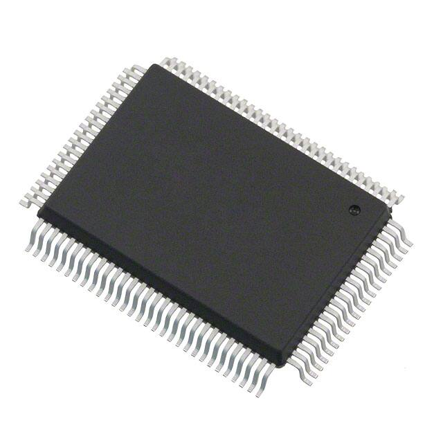
• Package: 10 x 10 x 2.0 mm 100-pin QFP
2
�xr
XRT91L32
STS-12/STM-4 OR STS-3/STM-1 SONET/SDH TRANSCEIVER
REV. 1.0.3
DLOOP
VDD3.3
CDRREFSEL
STS12/STS3
NC
TXDI0
TXDI1
GND
TXDI2
TXDI3
NC
TXIN4
TXDI5
GND
TXDI6
TXDI7
GND
NC
TXPCLK_IO
VDD
FIGURE 2. 100 QFP PIN OUT OF THE XRT91L32 (TOP VIEW)
81
82
83
84
85
86
87
88
89
90
91
92
93
94
95
96
97
98
99
100
1
2
3
4
5
6
7
8
9
10
11
12
13
14
15
16
17
18
19
20
21
22
23
24
25
26
27
28
29
30
XRT91L32
80
79
78
77
76
75
74
73
72
71
70
69
68
67
66
65
64
63
62
61
60
59
58
57
56
55
54
53
52
51
NC
NC
NC
NC
VDD3.3
GND
NC
NC
GND
AGND_RX
AGND_RX
AVDD3.3_RX
AVDD3.3_RX
AVDD3.3_RX
CAP2P
CAP2N
CAP1N
CAP1P
AVDD3.3_TX
NC
AGND_TX
AGND_TX
VDD3.3
NC
TTLREFCLK
GND
VDD3.3
LOSEXT
NC
CDRAUXREFCLK
VDD3.3
NC
NC
GND
RXDO0
RXD01
GND
RXDO2
RXDO3
GND
RXDO4
RXDO5
GND
RXDO6
RXDO7
GND
RXPCLKO
FRAMEPULSE
VDD3.3
NC
31
32
33
34
35
36
37
38
39
40
41
42
43
44
45
46
47
48
49
50
RLOOPS
VDD3.3
ALOOP
RESET
LOOPTIME
NC
NC
CMUFREQSEL
VDD_PECL
TXOP
TXON
GND
NC
NC
VDD_PECL
NC
DLOSDIS
GND
XRXCLKIP
XRXCLKIN
VDD_PECL
OOF
CDRDIS
RXIP
RXIN
NC
NC
VDD3.3
REFCLKP
REFCLKN
ORDERING INFORMATION
PART NUMBER
PACKAGE
OPERATING TEMPERATURE RANGE
XRT91L32IQ-F
100 Pin QFP
-40°C to +85°C
3
�xr
XRT91L32
REV. 1.0.3
STS-12/STM-4 OR STS-3/STM-1 SONET/SDH TRANSCEIVER
TABLE OF CONTENTS
GENERAL DESCRIPTION .................................................................................................1
APPLICATIONS ...........................................................................................................................................1
FIGURE 1. BLOCK DIAGRAM OF XRT91L32 ...................................................................................................................................... 1
FEATURES ......................................................................................................................................................2
FIGURE 2. 100 QFP PIN OUT OF THE XRT91L32 (TOP VIEW).......................................................................................................... 3
ORDERING INFORMATION.....................................................................................................................3
TABLE OF CONTENTS ............................................................................................................ I
PIN DESCRIPTIONS ..........................................................................................................4
.....................................................................................................................................................................4
HARDWARE CONTROL ....................................................................................................................................4
TRANSMITTER SECTION ..................................................................................................................................6
RECEIVER SECTION ........................................................................................................................................8
POWER AND GROUND ....................................................................................................................................9
1.0 FUNCTIONAL DESCRIPTION .............................................................................................................11
1.1 STS-12/STM-4 AND STS-3/STM-1 MODE OF OPERATION ......................................................................... 11
1.2 CLOCK INPUT REFERENCE FOR CLOCK MULTIPLIER (SYNTHESIZER) UNIT ...................................... 11
TABLE 1: CMU REFERENCE FREQUENCY OPTIONS (DIFFERENTIAL OR SINGLE-ENDED) ................................................................... 11
1.3 DATA LATENCY ............................................................................................................................................. 11
TABLE 2: DATA INGRESS TO DATA EGRESS LATENCY ....................................................................................................................... 11
2.0 RECEIVE SECTION .............................................................................................................................12
2.1 RECEIVE SERIAL INPUT ............................................................................................................................... 12
FIGURE 3. RECEIVE SERIAL INPUT INTERFACE BLOCK ..................................................................................................................... 12
2.2 RECIEVE SERIAL DATA INPUT TIMING ...................................................................................................... 13
FIGURE 4. RECEIVE HIGH-SPEED SERIAL DATA INPUT TIMING DIAGRAM .......................................................................................... 13
TABLE 3: RECEIVE HIGH-SPEED SERIAL DATA INPUT TIMING (STS-12/STM-4 OPERATION) ............................................................. 13
TABLE 4: RECEIVE HIGH-SPEED SERIAL DATA INPUT TIMING (STS-3/STM-1 OPERATION) ............................................................... 13
2.3 RECEIVE CLOCK AND DATA RECOVERY .................................................................................................. 14
TABLE 5: CLOCK DATA RECOVERY UNIT REFERENCE CLOCK SETTINGS ............................................................................................ 14
TABLE 6: CLOCK AND DATA RECOVERY UNIT PERFORMANCE .......................................................................................................... 15
2.3.1 INTERNAL CLOCK AND DATA RECOVERY BYPASS ............................................................................................ 15
FIGURE 5. INTERNAL CLOCK AND DATA RECOVERY BYPASS ............................................................................................................ 15
2.4 EXTERNAL RECEIVE LOOP FILTER CAPACITORS ................................................................................... 16
FIGURE 6. EXTERNAL LOOP FILTERS .............................................................................................................................................. 16
2.5 LOSS OF SIGNAL .......................................................................................................................................... 16
FIGURE 7. LOS DECLARATION CIRCUIT ........................................................................................................................................... 16
2.6 SONET FRAME BOUNDARY DETECTION AND BYTE ALIGNMENT RECOVERY .................................... 17
2.7 RECEIVE SERIAL INPUT TO PARALLEL OUTPUT (SIPO) ......................................................................... 17
FIGURE 8. SIMPLIFIED BLOCK DIAGRAM OF SIPO ........................................................................................................................... 17
2.8 RECEIVE PARALLEL OUTPUT INTERFACE ............................................................................................... 18
FIGURE 9. RECEIVE PARALLEL OUTPUT INTERFACE BLOCK ............................................................................................................. 18
2.9 DISABLE PARALLEL RECEIVE DATA OUTPUT UPON LOS ..................................................................... 18
2.10 RECEIVE PARALLEL DATA OUTPUT TIMING .......................................................................................... 19
FIGURE 10. RECEIVE PARALLEL OUTPUT TIMING ............................................................................................................................ 19
TABLE 7: RECEIVE PARALLEL DATA OUTPUT TIMING (STS-12/STM-4 OPERATION) ......................................................................... 19
TABLE 8: RECEIVE PARALLEL DATA OUTPUT TIMING (STS-3/STM-1 OPERATION) ........................................................................... 19
TABLE 9: PECL AND TTL RECEIVE OUTPUTS TIMING SPECIFICATION .............................................................................................. 20
3.0 TRANSMIT SECTION ..........................................................................................................................21
3.1 TRANSMIT PARALLEL INPUT INTERFACE ................................................................................................. 21
FIGURE 11. TRANSMIT PARALLEL INPUT INTERFACE BLOCK ............................................................................................................. 21
3.2 TRANSMIT PARALLEL DATA INPUT TIMING .............................................................................................. 22
FIGURE 12. TRANSMIT PARALLEL INPUT TIMING .............................................................................................................................. 22
TABLE 10: TRANSMIT PARALLEL DATA INPUT TIMING (STS-12/STM-4 OPERATION)......................................................................... 22
TABLE 11: TRANSMIT PARALLEL DATA INPUT TIMING (STS-3/STM-1 OPERATION)........................................................................... 22
3.3 TRANSMIT PARALLEL INPUT TO SERIAL OUTPUT (PISO) ...................................................................... 23
FIGURE 13. SIMPLIFIED BLOCK DIAGRAM OF PISO ......................................................................................................................... 23
3.4 CLOCK MULTIPLIER UNIT (CMU) AND RE-TIMER ..................................................................................... 23
TABLE 12: CLOCK MULTIPLIER UNIT PERFORMANCE ....................................................................................................................... 23
3.5 LOOP TIMING AND CLOCK CONTROL ........................................................................................................ 24
TABLE 13: LOOP TIMING AND CLOCK RECOVERY CONFIGURATIONS ................................................................................................. 24
I
�xr
XRT91L32
STS-12/STM-4 OR STS-3/STM-1 SONET/SDH TRANSCEIVER
REV. 1.0.3
FIGURE 14. LOOP TIMING MODE USING INTERNAL CDR OR AN EXTERNAL RECOVERED CLOCK ....................................................... 25
3.6 TRANSMIT SERIAL OUTPUT CONTROL ..................................................................................................... 25
FIGURE 15. TRANSMIT SERIAL OUTPUT INTERFACE BLOCK .............................................................................................................. 25
4.0 DIAGNOSTIC FEATURES ................................................................................................................... 26
4.1 SERIAL REMOTE LOOPBACK ..................................................................................................................... 26
FIGURE 16. SERIAL REMOTE LOOPBACK ......................................................................................................................................... 26
4.2 DIGITAL LOCAL LOOPBACK ....................................................................................................................... 26
FIGURE 17. DIGITAL LOCAL LOOPBACK ........................................................................................................................................... 26
4.3 ANALOG LOCAL LOOPBACK ...................................................................................................................... 27
FIGURE 18. ANALOG LOCAL LOOPBACK .......................................................................................................................................... 27
4.4 SPLIT LOOPBACK ......................................................................................................................................... 27
FIGURE 19. SPLIT LOOPBACK ......................................................................................................................................................... 27
4.5 EYE DIAGRAM ............................................................................................................................................... 28
FIGURE 20. STS-3/STM-1 EYE DIAGRAM ...................................................................................................................................... 28
FIGURE 21. STS-12/STM-4 EYE DIAGRAM .................................................................................................................................... 28
4.6 SONET JITTER REQUIREMENTS ................................................................................................................. 29
4.6.1 JITTER TOLERANCE: ................................................................................................................................................ 29
FIGURE 22. JITTER TOLERANCE MASK............................................................................................................................................ 29
FIGURE 23. XRT91L32 MEASURED JITTER TOLERANCE AT 622.08 MBPS STS-12/STM-4.............................................................. 30
FIGURE 24. XRT91L32 MEASURED JITTER TOLERANCE AT 155.52 MBPS STS-3/STM-1................................................................ 30
4.6.2 JITTER GENERATION................................................................................................................................................ 31
FIGURE 25. XRT91L32 MEASURED ELECTRICAL PHASE NOISE TRANSMIT JITTER GENERATION AT 622.08 MBPS STS-12/STM4 USING
’1010’ OUTPUT PATTERN ................................................................................................................................................. 31
5.0 ELECTRICAL CHARACTERISTICS ................................................................................................... 32
ABSOLUTE MAXIMUM RATINGS .................................................................................................................. 32
ABSOLUTE MAXIMUM POWER AND INPUT/OUTPUT RATINGS ......................................................... 32
POWER AND CURRENT DC ELECTRICAL CHARACTERISTICS .................................................................... 32
................................................................................................................................................................... 32
LVPECL AND LVTTL LOGIC SIGNAL DC ELECTRICAL CHARACTERISTICS...................................... 33
ORDERING INFORMATION .................................................................................................................. 34
PACKAGE DIMENSIONS ................................................................................................ 34
REVISION HISTORY ...................................................................................................................................... 35
II
�xr
XRT91L32
STS-12/STM-4 OR STS-3/STM-1 SONET/SDH TRANSCEIVER
REV. 1.0.3
PIN DESCRIPTIONS
L32
HARDWARE CONTROL
NAME
LEVEL
TYPE
PIN
DESCRIPTION
RESET
LVTTL
I
4
Remote Serial Loopback
Active "High." When this pin is pulled "High" , the internal state
machines are set to their default state.
"Low" = Normal Operation
"High" = Master Hardware Reset ( minimum 100nS)
STS12/STS3
LVTTL
I
97
Data Rate Selection
Selects SONET/SDH transmission and reception speed rate
"Low" = STS-3/STM-1 155.52 Mbps
"High" = STS-12/STM-4 622.08 Mbps
CMUFREQSEL
LVTTL
I
8
Clock Multiplier Unit Reference Frequency Select
This pin is used to select the frequency of the REFCLKP/N or
TTLREFCLK input to the CMU.
"Low" = 77.76 MHz reference clock
"High" = 19.44 MHz reference clock
CMUFREQSEL
STS12/
STS3
REFCLKP/N OR
TTLREFCLK
REFERENCE
DATA RATE
FREQUENCY
0
0
77.76 MHz
STS-3/STM-1
155.52 Mbps
0
1
77.76 MHz
STS-12/STM-4
622.08 Mbps
1
0
19.44 MHz
STS-3/STM-1
155.52 Mbps
1
1
19.44 MHz
STS-12/STM-4
622.08 Mbps
NOTE: REFCLKP/N or TTLREFCLK input should be generated
from an LVPECL/LVTTL crystal oscillator which has a
frequency accuracy better than 20ppm in order for the
transmitted data rate frequency to have the necessary
accuracy required for SONET systems..
4
�xr
XRT91L32
STS-12/STM-4 OR STS-3/STM-1 SONET/SDH TRANSCEIVER
REV. 1.0.3
NAME
LEVEL
TYPE
PIN
DESCRIPTION
CDRREFSEL
LVTTL
I
98
Clock and Data Recover Unit Reference Frequency Select
Selects the Clock and Data Recovery Unit reference frequency
based on the table below.
"Low" = CDR uses CMU’s reference clock
"High" = CDR reference clock from CDRAUXREFCLK
CDRREFSEL
STS12/
STS3
DATA RATE
CDR uses CMU’s reference clock
(see CMUFREQSEL pin)
0
NOTE:
CDRAUXREFCLK
FREQUENCY
1
0
77.76 MHz
STS-3/STM-1
155.52 Mbps
1
1
77.76 MHz
STS-12/STM-4
622.08 Mbps
CDRAUXREFCLK requires accuracy of 77.76 MHz
+/- 500ppm.
LOOPTIME
LVTTL
I
5
Loop Timing Mode
When the loop timing mode is activated the external reference
clock to the input of the Retimer is replaced with the high-speed
recovered receive clock from the CDR.
"Low" = Disabled
"High" = Loop timing Activated
CDRDIS
LVTTL
I
23
Clock and Data Recovery Unit Disable
Active "High." Disables internal Clock and Data Recovery unit.
Received serial data bypasses the integrated CDR block.
RXINP/N is then sampled on the rising edge of externally
recovered differential clock XRXCLKIP/N coming from the optical module.
"Low" = Internal CDR unit is Enabled
"High" = Internal CDR unit is Disabled and Bypassed
RLOOPS
LVTTL
I
1
Serial Remote Loopback
The serial remote loopback mode interconnects the receive
serial data input to the transmit serial data output. If serial
remote loopback is enabled, the 8-bit parallel transmit data
input is ignored while the 8-bit parallel receive data output is
maintained.
"Low" = Disabled
"High" = Serial Remote Loopback Mode Enabled
NOTE: DLOOP and RLOOPS can be enabled simultaneously
to achieve a dual loopback diagnostic feature in normal
operation.
NC
No Connect
-
6,7,13, NOTE: No connect
14,16,26,
27,32,33,
50,52,57,
61,73,74,
77,78,79,
80,83,90,
96
5
�xr
XRT91L32
STS-12/STM-4 OR STS-3/STM-1 SONET/SDH TRANSCEIVER
REV. 1.0.3
NAME
LEVEL
TYPE
PIN
DESCRIPTION
ALOOP
LVTTL
I
3
Analog Local Loopback
This loopback feature serializes the 8-bit parallel transmit data
input and presents the data to the transmit serial output and in
addition it also internally routes the serialized data back to the
Clock and Data Recovery block for serial to parallel conversion.
The received serial data input is ignored.
"Low" = Disabled
"High" = Analog Local Loopback Mode Enabled
DLOOP
LVTTL
I
100
DLOOP Local Loopback
This digital loopback mode interconnects the 8-bit parallel
transmit data input and TXCLK to the 8-bit parallel receive data
output and receive RXCLK respectively while maintaining the
transmit serial data output. If digital loopback is enabled, the
receive serial data input is ignored.
"Low" = Disabled
"High" = Digital Local Loopback Mode Enabled
NOTE: DLOOP and RLOOPS can be enabled simultaneously
to achieve a dual loopback diagnostic feature in normal
operation.
TRANSMITTER SECTION
NAME
LEVEL
TYPE
PIN
DESCRIPTION
TXDI0
TXDI1
TXDI2
TXDI3
TXDI4
TXDI5
TXDI6
TXDI7
LVTTL
I
95
94
92
91
89
88
86
85
Transmit Parallel Data Input
Transmit Parallel Clock Output Operation
The 77.76 Mbps (STS-12/STM-4) / 19.44 Mbps (STS-3/STM-1)
8-bit parallel transmit data should be applied to the transmit
parallel bus and simultaneously referenced to the rising edge of
the TXPCLK_IO clock output. The 8-bit parallel interface is multiplexed into the transmit serial output interface with the MSB
first (TXDI[7:0]).
Alternate Transmit Parallel Clock Input Operation
When operating is this mode, TXPCLK_IO is no longer a parallel clock output reference but reverses direction and serves as
the parallel transmit clock input reference for the PISO (Parallel
Input to Serial Output) block. The 77.76 Mbps (STS-12/STM-4)
/ 19.44 Mbps (STS-3/STM-1) 8-bit parallel transmit data should
be applied to the transmit parallel bus and simultaneously referenced to the rising edge of the TXPCLK_IO clock input.
TXOP
TXON
LVPECL Diff
O
10
11
Transmit Serial Data Output
The transmit serial data stream is generated by multiplexing the
8-bit parallel transmit data input into a 622.08 Mbps STS-12/
STM-4 or 155.52 Mbps STS-3/STM-1 serial data stream.
6
�xr
XRT91L32
STS-12/STM-4 OR STS-3/STM-1 SONET/SDH TRANSCEIVER
REV. 1.0.3
TRANSMITTER SECTION
NAME
LEVEL
TYPE
PIN
DESCRIPTION
TXPCLK_O
LVTTL
O
82
Transmit Parallel Clock Output (77.76/19.44 MHz)
Transmit Parallel Clock Output Operation
This pin will output a 77.76 MHz (STS-12/STM-4) or 19.44 MHz
(STS-3/STM-1) clock output reference for the 8-bit parallel
transmit data input TXDI[7:0]. This clock is used by the framer/
mapper device to present the TXDI[7:0] data which the
XRT91L32 will latch on the rising edge of this clock. This
enables the framer/mapper device and the XRT91L32 transceiver to be in synchronization.
REFCLKP
REFCLKN
LVPECL Diff
I
29
30
Reference Clock Input (77.76 MHz or 19.44 MHz)
This differential clock input reference is used for the transmit
clock multiplier unit (CMU) and clock data recovery (CDR) to
provide the necessary high speed clock reference for this
device. It will accept either a 77.76 MHz or a 19.44 MHz Differential LVPECL clock source. Pin CMUFREQSEL determines
the value used as the reference. See Pin CMUFREQSEL for
more details. REFCLKP/N inputs are internally biased to 1.65V.
NOTE:
TTLREFCLK
LVTTL
I
56
In the event that TTLREFCLK LVTTL input is used
instead of these differential inputs for clock reference,
the REFCLKP should be tied to ground.
Auxillary Reference Clock Input (77.76 MHz or 19.44 MHz)
This LVTTL clock input reference is used for the transmit clock
multiplier unit (CMU) and clock data recovery (CDR) to provide
the necessary high speed clock reference for this device. It will
accept either a 77.76 MHz or a 19.44 MHz LVTTL clock source.
Pin CMUFREQSEL determines the value used as the reference. See Pin CMUFREQSEL for more details.
NOTE: In the event that REFCLKP/N differential inputs is used
instead of this LVTTL input for clock reference, the
TTLREFCLK should be tied to ground.
7
�xr
XRT91L32
STS-12/STM-4 OR STS-3/STM-1 SONET/SDH TRANSCEIVER
REV. 1.0.3
RECEIVER SECTION
NAME
LEVEL
TYPE
PIN
DESCRIPTION
RXDO0
RXDO1
RXDO2
RXDO3
RXDO4
RXDO5
RXDO6
RXDO7
LVTTL
O
35
36
38
39
41
42
44
45
Receive Parallel Data Output
77.76 Mbps (STS-12/STM-4) / 19.44 Mbps (STS-3/STM-1)
8-bit parallel receive data output is updated simultaneously on
the rising edge of the RXPCLKO output. The 8-bit parallel interface is de-multiplexed from the receive serial data input MSB
first (RXDO[7:0]). The XRT91L32 will output the data on the
rising edge of this clock.
RXIP
RXIN
Diff LVPECL
I
24
25
Receive Serial Data Input
The differential receive serial data stream of 622.08 Mbps
STS-12/STM-1 or 155.52 Mbps STS-3/STM-1 is applied to
these input pins.
XRXCLKIP
XRXCLKIN
Diff LVPECL
I
19
20
External Recovered Receive Clock Input
The differential receive serial data stream of 622.08 Mbps
STS-12/STM-1 or 155.52 Mbps STS-3/STM-1 is sampled on
the rising edge of this externally recovered differential clock
coming from the optical module. It is used when the internal
CDR unit is disabled and bypassed by the CDRDIS pin.
NOTE: In the event that XRXCLKIP/N differential input pins are
unused, XRXCLKIP should be tied to VCC with a 1k
Ohm pull-up and XRXCLKIN should be tied to Ground
with a 1k Ohm pull-down.
RXPCLKO
LVTTL
O
47
Receive Parallel Clock Output (77.76 MHz or 19.44 MHz)
77.76 MHz (STS-12/STM-4) or 19.44 MHz (STS-3/STM-1)
clock output reference for the 8-bit parallel receive data output
RXDO[7:0]. The parallel received data output bus will be
updated on the falling edge of this clock.
CDRAUXREFCLK
LVTTL
I
51
Clock and Data Recovery Auxillary Reference Clock
77.76 MHz ± 500 ppm auxillary reference clock for the CDR.
NOTE: In the event that CDRAUXREFCLK LVTTL input pin is
unused, CDRAUXREFCLK should be tied to ground.
OOF
LVTTL
I
22
Out of Frame Input Indicator
This level sensitive input pin is used to initiate frame detection
and byte alignment recovery when OOF is declared by the
downstream device. When this pin is held High, FRAMEPULSE will pulse for a single RXPCLKO period upon the detection of every third frame alignment A2 byte in the incoming
SONET/SDH Frame.
"Low" = Normal Operation
"High" = OOF Indication initiating frame detection and byte
boundary recovery and activating FRAMEPULSE
FRAMEPULSE
LVTTL
O
48
Sonet Frame Alignment Pulse
This pin will generate a single pulse for an RXPCLKO clock
period upon the detection of the third frame alignment A2 byte
whenever the OOF input pin is held High. The parallel received
data output bus will then be byte aligned to this newly recovered SONET/SDH frame.
8
�xr
XRT91L32
STS-12/STM-4 OR STS-3/STM-1 SONET/SDH TRANSCEIVER
REV. 1.0.3
NAME
LEVEL
TYPE
PIN
DESCRIPTION
CAP1P
CAP2P
Analog
-
63
66
CDR Non-Inverting External Feeback Capacitor
C1 = 0.47μF ± 10% tolerance
(Isolate from noise and place close to pin)
CAP1N
CAP2N
Analog
-
64
65
CDR Inverting External Feeback Capacitor
C2 = 0.47μF ± 10% tolerance
(Isolate from noise and place close to pin)
DLOSDIS
LVTTL
I
17
LOS (Los of Signal) Detect Disable
Disables internal LOS monitoring and automatic muting of
RXDO[7:0] upon LOS detection (according to gating shown in
Figure 7.) LOS is declared when a string of 128 consecutive
zeros occur on the line. LOS condition is cleared when the 16
or more pulse transitions is detected for 128 bit period sliding
window.
"Low" = Monitor and Mute received data upon LOS declaration
"High" = Disable internal LOS monitoring (see Figure 7 for logic
operation.)
LOSEXT
SE-LVPECL
I
53
LOS or Signal Detect Input from Optical Module
Active "Low." When active, this pin can force the received data
output bus RXDO[7:0] to a logic state of ’0’ per Figure 7.
"Low" = Forced LOS
"High" = Normal Operation
POWER AND GROUND
NAME
TYPE
PIN
DESCRIPTION
VDD3.3
PWR
2,28,31,49,54,
58,76,99,81
3.3V CMOS Power Supply
VDD3.3 should be isolated from the analog VDD power supplies.
Use a ferrite bead along with an internal power plane separation.
The VDD3.3 power supply pins should have bypass capacitors to
the nearest ground. For best results, refer to Application notes
about general board layout guidelines.
AVDD3.3_TX
PWR
62
Analog 3.3V Transmitter Power Supply
AVDD3.3_TX should be isolated from the digital power supplies.
For best results, use a ferrite bead along with an internal power
plane separation. The AVDD3.3_TX power supply pins should
have bypass capacitors to the nearest ground.
AVDD3.3_RX
PWR
67,,68,69
Analog 3.3V Receiver Power Supply
AVDD3.3_RX should be isolated from the digital power supplies.
For best results, use a ferrite bead along with an internal power
plane separation. The AVDD3.3_RX power supply pins should
have bypass capacitors to the nearest ground.
VDD_LVPECL
PWR
9,15,21
3.3V Input/Output LVPECL Bus Power Supply
These pins require a 3.3V potential voltage for properly biasing
the Differential LVPECL input and output pins.
AGND_TX
PWR
59,60
Transmitter Analog Ground for 3.3V Analog Power Supplies
It is recommended that all ground pins of this device be tied
together.
9
�xr
XRT91L32
STS-12/STM-4 OR STS-3/STM-1 SONET/SDH TRANSCEIVER
NAME
TYPE
PIN
AGND_RX
PWR
70,71
GND
GND
REV. 1.0.3
DESCRIPTION
Receiver Analog Ground for 3.3V Analog Power Supplies
It is recommended that all ground pins of this device be tied
together.
12,18,34,37,40,43,46,55, Power Supply and Thermal Ground
72,75,84,87,93
It is recommended that all ground pins of this device be tied
together.
10
�xr
XRT91L32
STS-12/STM-4 OR STS-3/STM-1 SONET/SDH TRANSCEIVER
REV. 1.0.3
1.0 FUNCTIONAL DESCRIPTION
The XRT91L32 transceiver is designed to operate with a SONET Framer/ASIC device and provide a highspeed serial interface to optical networks. The transceiver converts 8-bit parallel data running at 77.76 Mbps
(STS-12/STM-4) or 19.44 Mbps (STS-3/STM-1) to a serial Differential LVPECL bit stream at 622.08 Mbps or
155.52 Mbps and vice-versa. It implements a clock multiplier unit (CMU), SONET/SDH serialization/deserialization (SerDes), receive clock and data recovery (CDR) unit and a SONET/SDH frame and byte
boundary detection circuit. The transceiver is divided into Transmit and Receive sections and is used to
provide the front end component of SONET equipment, which includes primarily serial transmit and receive
functions.
1.1
STS-12/STM-4 and STS-3/STM-1 Mode of Operation
Functionality of the transceiver can be configured by using the appropriate signal level on the STS-12/STS-3
pin. STS-3/STM-1 mode is selected by pulling STS-12/STS-3 "Low" as described in the Hardware Pin
Descriptions. However, if STS-12/STM-4 mode is desired, it is selected by pulling STS-12/STS-3 "High."
Therefore, the following sections describe the functionality rather than how each function is controlled. Hence,
the hardware Pin and the Register Bit Descriptions focus on device configuration.
1.2
Clock Input Reference for Clock Multiplier (Synthesizer) Unit
The XRT91L32 can accept both a 19.44 MHz or a 77.76 MHz Differential LVPECL clock input at REFCLKP/N
or a Single-Ended LVTTL clock at TTLREFCLK as its internal timing reference for generating higher speed
clocks. The REFCLKP/N or TTLREFCLK input should be generated from an LVPECL/LVTTL crystal oscillator
which has a frequency accuracy better than 20ppm in order for the transmitted data rate frequency to have the
necessary accuracy required for SONET systems. The reference clock can be provided with one of two
frequencies chosen by CMUFREQSEL. The reference frequency options for the XRT91L32 are listed in
Table 1.
TABLE 1: CMU REFERENCE FREQUENCY OPTIONS (DIFFERENTIAL OR SINGLE-ENDED)
REFCLKP/N OR TTLREFCLK
CMUFREQSEL
STS12/STS3
0
0
77.76 MHz
STS-3/STM-1
155.52 Mbps
0
1
77.76 MHz
STS-12/STM-4
622.08 Mbps
1
0
19.44 MHz
STS-3/STM-1
155.52 Mbps
1
1
19.44 MHz
STS-12/STM-4
622.08 Mbps
1.3
REFERENCE FREQUENCY
DATA RATE
Data Latency
Due to different operating modes and data logic paths through the device, there is an associated latency from
data ingress to data egress. Table 2 specifies the data latency for a typical path.
TABLE 2: DATA INGRESS TO DATA EGRESS LATENCY
MODE OF
OPERATION
Thru-mode
DATA PATH
CLOCK REFERENCE RANGE OF CLOCK
CYCLES
MSB at RXIP/N to data on RXDO[7:0]
Serial Remote Loopback MSB at RXIP/N to MSB at TXOP/N
11
Recoved RXIP/N Clock
25 to 35
Recoved RXIP/N Clock
2 to 4
�XRT91L32
STS-12/STM-4 OR STS-3/STM-1 SONET/SDH TRANSCEIVER
xr
REV. 1.0.2
2.0 RECEIVE SECTION
The receive section of XRT91L32 include the inputs RXIP/N, followed by the clock and data recovery unit
(CDR) and receive serial-to-parallel converter. The receiver accepts the high speed Non-Return to Zero (NRZ)
serial data at 622.08 Mbps or 155.52 Mbps through the input interfaces RXIP/N. The clock and data recovery
unit recovers the high-speed receive clock from the incoming scrambled NRZ data stream. The recovered
serial data is converted into an 8-bit-wide, 77.76 Mbps or 19.44 Mbps parallel data and presented to the
RXDO[7:0] parallel interface. This parallel interface is designed for Single-Ended LVTTL operation. A divideby-8 version of the high-speed recovered clock RXPCLKOP/N, is used to synchronize the transfer of the 8-bit
RXDO[7:0] data with the receive portion of the framer/mapper device. Upon initialization or loss of signal or
loss of lock, the external reference clock signal of 19.44 MHz or 77.76 MHz is used to start-up the clock
recovery phase-locked loop for proper operation. In certain applications, the CDR block on the XRT91L32 can
be disabled and bypassed by enabling the CDRDIS pin to permit the flexibility of using an externally recovered
receive clock thru the XRXCLKIP/N pins.7
2.1
Receive Serial Input
The receive serial inputs are applied to RXIP/N. The receive serial inputs can be AC or DC coupled to an
optical module or an electrical interface. A simplified AC coupling block diagram is shown in Figure 3.(Also,
FIGURE 3. RECEIVE SERIAL INPUT INTERFACE BLOCK
Install terminators close to
RXIP and RXIN pins
82 Ohm
RXIP
SFP, Optical Module
RXIN
XRT91L32
STS-12/STM-4
or
STS-3/STM-1
Transceiver
Optical Fiber
1KOhm
Tie unused differential input pins
to VCC and GND
XRXCLKIP
XRXCLKIN
Internally
AC coupled
130 Ohm
1KOhm
(optional)
refer to application note TAN-9132.)
NOTE: Some optical modules integrate AC coupling capacitors within the module. AC or DC coupling is largely specific to
system design and optical module of choice.
12
�xr
XRT91L32
STS-12/STM-4 OR STS-3/STM-1 SONET/SDH TRANSCEIVER
REV. 1.0.2
2.2
Recieve Serial Data Input Timing
The received High-Speed Serial Differential Data Input must adhere to the set-up and hold time timing
specifications below.
FIGURE 4. RECEIVE HIGH-SPEED SERIAL DATA INPUT TIMING DIAGRAM
tRXCLK
XRXCLKIP
XRXCLKIN
tRX_HD
tRX_SU
RXIP
RXIN
TABLE 3: RECEIVE HIGH-SPEED SERIAL DATA INPUT TIMING (STS-12/STM-4 OPERATION)
SYMBOL
PARAMETER
MIN
TYP
MAX
1.608
UNITS
tRXCLK
Receive external recovered clock period
ns
tRX_SU
Serial data setup time with respect to XRXCLKIP/N
400
ps
tRX_HD
Serial data hold time with respect to XRXCLKIP/N
100
ps
TABLE 4: RECEIVE HIGH-SPEED SERIAL DATA INPUT TIMING (STS-3/STM-1 OPERATION)
SYMBOL
PARAMETER
MIN
TYP
UNITS
tRXCLK
Receive external recovered clock period
tRX_SU
Serial data setup time with respect to XRXCLKIP/N
1.5
ns
tRX_HD
Serial data hold time with respect to XRXCLKIP/N
1.5
ns
13
6.43
MAX
ns
�xr
XRT91L32
STS-12/STM-4 OR STS-3/STM-1 SONET/SDH TRANSCEIVER
2.3
REV. 1.0.2
Receive Clock and Data Recovery
The clock and data recovery (CDR) unit accepts the high speed NRZ serial data from the Differential LVPECL
receiver and generates a clock that is the same frequency as the incoming data. The clock recovery can either
utilize the transmitter’s CMU reference clock from either REFCLKP/N or TTLREFCLK or it can use
independent clock source CDRAUXREFCLK to train and monitor its clock recovery PLL. Initially upon startup,
the PLL locks to the local reference clock within ±500 ppm. Once this is achieved, the PLL then attempts to
lock onto the incoming receive data stream. Whenever the recovered clock frequency deviates from the local
reference clock frequency by more than approximately ±500 ppm, the clock recovery PLL will switch and lock
back onto the local reference clock. Whenever a Loss of Lock or a Loss of Signal event occurs, the CDR will
continue to supply a receive clock (based on the local reference) to the framer/mapper device. When the
LOSEXT is asserted by the optical module or when LOS is detected, the receive parallel data output will be
forced to a logic zero state for the entire duration that a LOS condition is detected. This acts as a receive data
mute upon LOS function to prevent random noise from being misinterpreted as valid incoming data. When the
LOSEXT becomes inactive and the recovered clock is determined to be within ±500 ppm accuracy with respect
to the local reference source and LOS is no longer declared, the clock recovery PLL will switch and lock back
onto the incoming receive data stream. Table 5 shows Clock and Data Recovery reference clock settings.
Table 6 specifies the Clock and Data Recovery Unit performance characteristics.
TABLE 5: CLOCK DATA RECOVERY UNIT REFERENCE CLOCK SETTINGS
CMUFREQSEL CDRREFSEL
STS12/
STS3
REFCLKP/N1OR
TTLREFCLK1
FREQUENCY (MHZ)
CDRAUXREFCLK2
FREQUENCY (MHZ)
CDR OUTPUT
FREQUENCY (MHZ)
0
0
0
77.76 MHz
not used
155.52
0
0
1
77.76 MHz
not used
622.08
1
0
0
19.44 MHz
not used
155.52
1
0
1
19.44 MHz
not used
622.08
X
1
0
not referenced by CDR
77.76 MHz
155.52
X
1
1
not referenced by CDR
77.76 MHz
622.08
1
Requires frequency accuracy better than 20ppm in order for the transmitted data rate frequency to have the necessary
accuracy required for SONET systems.
2
CDRAUXREFCLK requires accuracy of 77.76 MHz +/- 500ppm.
14
�xr
XRT91L32
STS-12/STM-4 OR STS-3/STM-1 SONET/SDH TRANSCEIVER
REV. 1.0.2
TABLE 6: CLOCK AND DATA RECOVERY UNIT PERFORMANCE
NAME
PARAMETER
MIN
TYP
40
MAX
UNITS
60
%
REFDUTY
Reference clock duty cycle
REFJIT
Reference clock jitter (rms) with 19.44 MHz reference1
5
ps
REFJIT
Reference clock jitter (rms) with 77.76 MHz reference1
13
ps
REFTOL
Reference clock frequency tolerance2
-20
+20
ppm
TOLJIT
Input jitter tolerance with 1 MHz < f < 20 MHz PRBS pattern
0.3
OCLKFREQ
Frequency output
620
624
MHz
OCLKDUTY
Clock output duty cycle
40
60
%
0.4
UI
Jitter specification is defined using a 12kHz to 1.3/5MHz LP-HP single-pole filter.
1
These reference clock jitter limits are required for the outputs to meet SONET system level jitter requirements (