11-MD127
Version Issue Date File Name Total Pages : A.008 : 2006/08/31 : SP-MD127-A.008.doc : 10
Low-saturation, Low-voltage 2 Channels Bi-directional Motor Driver
新竹市展業一路 9 號 7 樓之 1 SILICON TOUCH TECHNOLOGY INC.
9-7F-1, Prosperity Rd I, Science-Based Industrial Park Hsinchu, Taiwan, R.O.C. Tel:886-3-5645656 Fax:886-3-5645626
�點晶科技股份有限公司
SILICON TOUCH TECHNOLOGY INC.
11-MD127
11-MD127 Low-saturation, Low-voltage 2 Channels Bi-directional Motor Driver
General Specifications
The device is a two-channel low-saturation bi-directional motor driver IC. The design is optimal for 2-dc motor or stepper-motor applications, such as driving shutter/iris on cameras and other motor applications on portable devices.
Features and Benefits
Low voltage operation ( VDD min = 2.0V ) Low saturation voltage ( Upper transistor + low transistor residual voltage; 0.46V typ. at 400mA) Low input current Low operating current High output sinking and driving capability Ultra-small, thin, highly reliable package (WLCSP, MSOP-10 and DFN-10) Thermal shutdown protection
Pin Assignment
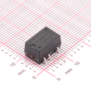
MSOP-10
V DD IN4 IN3 IN1 IN2
1 2 3 4 5 10 9
O4 O3 O1 O2 GND
PIN NO. PIN NAME 1 2 3 4 5 6 VDD IN4 IN3 IN1 IN2 GND O2 O1 O3 O4
DESCRIPTION Power supply pin Input pin that determines driving mode. Input pin that determines driving mode. Input pin that determines driving mode. Input pin that determines driving mode. Ground pin Output sinking / driving pin Output sinking / driving pin Output sinking / driving pin Output sinking / driving pin. Version: A.008
1 1-MD127
8 7 6
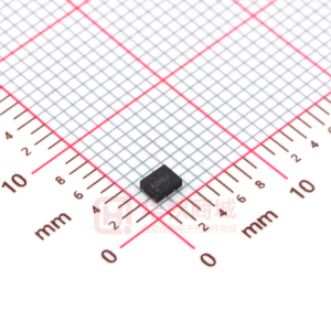
DFN-10
VDD IN4 IN3 IN1 IN2 1 2 3 4 5 10 9 8 7 6 O4 O3 O1 O2 GND
7 8 9 10
SP-MD127-A.008(MSOP10,DFN10,WLCSP) -1-
�點晶科技股份有限公司
SILICON TOUCH TECHNOLOGY INC.
11-MD127
WLCSP
TOP VIEW a b c d
1
GND
OUT1
OUT3
OUT4
2
OUT2
7XX
IN1 IN3
IN4
3
IN2
VDD
PIN NO. PIN NAME a1 a2 a3 b1 b3 c1 c3 d1 d2 d3 GND OUT2 IN2 OUT1 IN1 OUT3 IN3 OUT4 IN4 VDD
DESCRIPTION Ground pin Output sinking / driving pin Input pin that determines driving mode. Output sinking / driving pin Input pin that determines driving mode. Output sinking / driving pin Input pin that determines driving mode. Output sinking / driving pin. Input pin that determines driving mode. Power supply pin
SP-MD127-A.008(MSOP10,DFN10,WLCSP) -2-
Version: A.008
�點晶科技股份有限公司
SILICON TOUCH TECHNOLOGY INC.
11-MD127
Absolute Maximum Ratings ( Unless otherwise noted, TA= 25℃ )
Characteristic Supply Voltage Input Voltage Maximum Output Current/Channel (DFN,MSOP) Maximum Output Current/Channel (WLCSP) Power Dissipation (IC) Power Dissipation (PCB mounted) Operating Temperature Range Storage Temperature Range Symbol VDD VIN I OUT1 I OUT2 PD PD-PCB TOPR TSTG Rating 5.5 VDD+0.4 400 250 486 870 -40 ~ 125 -65 ~ 150 Unit V V mA mA mW °C °C
Electrical Characteristic (Unless otherwise noted, TA= 25℃ & VDD = 3V )
Characteristic Supply Voltage Supply Current Sym. VDD IDD0 IDD1 VIN1,IN2,IN3,IN4=0V VIN1,IN2,IN3,IN4≠0V Condition Limit Min. 2.0 Typ. 3 0.1 0.2 Max. 5.5 10 0.5 Unit V μA mA
IN 1 / IN 2 / IN3 / IN4 Input Terminal ( TJ = 25℃) Input Voltage “H” Input Voltage “L” Input Current “H” Input Current “L” VIH VIL IIH IIL VIN = VDD VIN = 0 V 0.5*VDD -0.4 VDD+0.4 0.2*VDD ±5 ±5 V V μA μA
O1 / O2 / O3 / O4 Output Terminal ( TJ = 25℃) Output Voltage (upper + lower) VOUT1 VOUT2 VOUT3 IOUT = 100 mA IOUT = 200 mA IOUT = 400 mA 0.12 0.28 0.46 0.2 0.4 0.7 V V V
Thermal Protection Circuit Protection Temperature TTSD VIN1, IN2, IN3, IN4 =H 150 ℃
SP-MD127-A.008(MSOP10,DFN10,WLCSP) -3-
Version: A.008
�點晶科技股份有限公司
SILICON TOUCH TECHNOLOGY INC.
11-MD127
Truth Table
IN1 / IN3 L H L H IN2 / IN4 L L H H O1 / O3 OFF H L — O2 / O4 OFF L H — Standby Forward Reverse Keep the previous mode (Forward / Reverse) Mode
Note: “—” indicates a “don’t care” input.
Block Diagram & Application Circuit
1.Shutter & Iris application
VDD 1 O1 4 8 M1 IN2 5 7 O2
10μF
IN1
Control Block
O3 IN3 3 9 M2 IN4 2 10 O4
6 GND
2. Stepping motor for 1-2 phase excitation
VDD 1 O1 4 8
Stepping Motor 10μF
IN1
IN2
5
7
Control Block
IN3 3 9
O2
O3
IN4
2
10
O4
GND
6
SP-MD127-A.008(MSOP10,DFN10,WLCSP) -4-
Version: A.008
�點晶科技股份有限公司
SILICON TOUCH TECHNOLOGY INC.
11-MD127
Notes Standby
IN1 IN2 IN3 IN4 O1 O2 O3 O4 L L L L OFF OFF OFF OFF H L L L H L OFF OFF H L H L H L H L L L H L OFF OFF H L L H H L L H H L L H L L L H OFF OFF L H L H L H L H L L L H OFF OFF L H H L L H H L L H H H Keep the previous output state H H Note: “—” indicates a “don’t care” input.
1-2 phase excitation
Application Notes
The power dissipated by the IC varies widely with the supply voltage, the output current, and loading. It is important to ensure the application does not exceed the allowable power dissipation of the IC package. The recommended motor driver power dissipation versus temperature is depicted as follows: Pdmax VS Ta
1000 Power Dissipation(mW) 900 800 700 600 JESD51-3 500 400 300 200 100 0 25 50 75 100 125
JESD51-7 870mW
486mW
Ambient Temperature ( ℃ )
SP-MD127-A.008(MSOP10,DFN10,WLCSP) -5-
Version: A.008
�點晶科技股份有限公司
SILICON TOUCH TECHNOLOGY INC.
11-MD127
Typical Performance Curve
VSAT VS IOUT Output Saturation Voltage V SAT(V)
0.7 0.6 0.5 0.4 0.3 0.2 0.1 0.0 0.1 0.2 0.3 0.4 0.5
VDD=3V VDD=3V VDD=5V VDD=5V
VIN=VDD
IDD VS VDD
1.2 1.1 1.0 0.9 0.8 0.7 0.6 0.5 0.4 0.3 0.2 0.1 0
VEN=VDD
Current Drain I DD (mA)
0.5 1 1.5 2 2.5 3 3.5 4 4.5 5 5.5 6 6.5 Power Supply Voltage V DD (V)
Output Current I OUT(A)
Package Specifications MSOP-10
(10-pin MSOP )
E1
E C
θ L D 12°(4X)
A2
A
A1 y b e
Dimensions in Millimeter SYMBOL A A1 A2 b C D E E1 e L Y θ MIN 0.81 0.00 0.76 0.15 0.13 2.90 4.80 2.90 - 0.40 - 0° NOM 0.92 - 0.86 0.20 0.15 3.00 4.90 3.00 0.50 0.53 - - MAX 1.07 0.10 0.97 0.30 0.23 3.10 5.00 3.10 - 0.66 0.10 6°
Dimensions in Inches MIN 0.032 0.000 0.030 0.006 0.005 0.114 0.189 0.114 - 0.016 - 0° NOM 0.036 - 0.034 0.008 0.006 0.118 0.193 0.118 0.0197 0.021 - - MAX 0.042 0.004 0.038 0.012 0.009 0.122 0.197 0.122 - 0.026 0.004 6°
SP-MD127-A.008(MSOP10,DFN10,WLCSP) -6-
Version: A.008
�點晶科技股份有限公司
SILICON TOUCH TECHNOLOGY INC.
11-MD127
DFN-10
SYMBOL A A1 A3 b D D1 E E1 L e e1 MIN. 0.70 0.00 0.18 2.90 2.10 2.90 1.10 0.45
DIMENSION (mm) NOM. 0.75 0.02 0.203 REF 0.25 3.00 2.20 3.00 1.20 0.55 0.50 BASIC 2.00 BASIC
MAX. 0.80 0.05 0.30 3.10 2.30 3.10 1.30 0.65
MIN. 28 0 7 114 83 114 86 18
DIMENTION (mil) NOM. 30 0.8 8 REF 10 118 87 118 87 22 20 BASIC 79 BASIC
MAX. 32 2 12 122 91 122 91 26
SP-MD127-A.008(MSOP10,DFN10,WLCSP) -7-
Version: A.008
�點晶科技股份有限公司
SILICON TOUCH TECHNOLOGY INC.
11-MD127
WLCSP
BOTTOM VIEW (Ball side) d c b a
TOP VIEW (Marking side)
1 D1 2 b 3 b ZD D
7XX
E A2 A1 ZE E1
A
XX is the run code.
SYMBOL A A1 A2 b D D1 E E1 ZD ZE MIN. 0.45 0.08 0.37 0.26 1.40 1.90
DIMENSION (mm) NOM. 0.50 0.10 0.40 0.28 1.50 0.50 2.00 0.50 0.25 0.25
MAX. 0.55 0.12 0.43 0.30 1.60 2.10
SP-MD127-A.008(MSOP10,DFN10,WLCSP) -8-
Version: A.008
�點晶科技股份有限公司
SILICON TOUCH TECHNOLOGY INC.
11-MD127
The products listed herein are designed for ordinary electronic applications, such as electrical appliances, audio-visual equipment, communications devices and so on. Hence, it is advisable that the devices should not be used in medical instruments, surgical implants, aerospace machinery, nuclear power control systems, disaster/crime-prevention equipment and the like. Misusing those products may directly or indirectly endanger human life, or cause injury and property loss. Silicon Touch Technology, Inc. will not take any responsibilities regarding the misusage of the products mentioned above. Anyone who purchases any products described herein with the above-mentioned intention or with such misused applications should accept full responsibility and indemnify. Silicon Touch Technology, Inc. and its distributors and all their officers and employees shall defend jointly and severally against any and all claims and litigation and all damages, cost and expenses associated with such intention and manipulation.
SP-MD127-A.008(MSOP10,DFN10,WLCSP) -9-
Version: A.008
�