DATA SHEET
AAT2713
Low Noise, Dual 600mA Step-Down Converter with Synchronization
General Description
Features
The AAT2713 is a high efficiency dual synchronous stepdown converter for applications where power efficiency,
thermal performance and solution size are critical. Input
voltage ranges from 2.7V to 5.5V, making it ideal for
systems powered by single-cell lithium-ion/polymer batteries. The AAT2713 incorporates a unique low noise
architecture which reduces ripple and spectral noise.
•
•
•
•
Each converter is capable of 600mA output current and
has its own enable pin. Efficiency of the converters is
optimized over full load range. Total no load quiescent
current is 70μA, allowing high efficiency even under light
load conditions.
The integrated power switches are controlled by pulse
width modulation (PWM) with a 1.7MHz typical switching
frequency at full load, which minimizes the size of external components. Fixed frequency, low noise operation
can be forced by a logic signal on the MODE pin.
Furthermore, an external clock can be used to synchronize the switching frequency of both converters.
A phase shift pin (PS) is available to operate the two
converters 180° out of phase at heavy load to achieve
low input ripple.
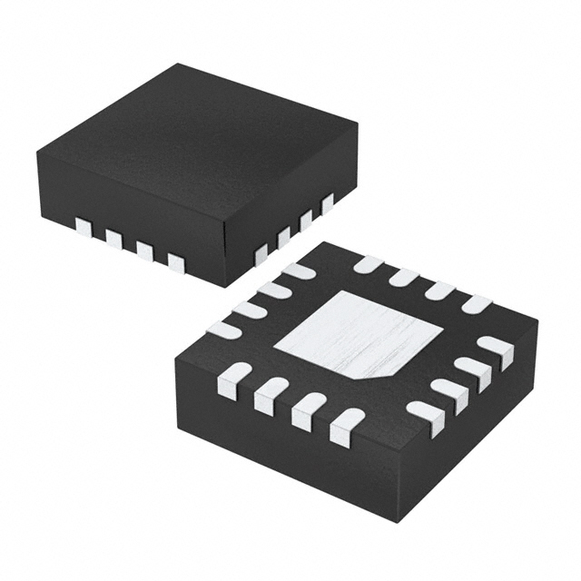
The AAT2713 is available in a Pb-free, thermally
enhanced 16-pin QFN33 package and is specified for
operation over the -40°C to +85°C temperature range.
•
•
•
•
•
•
•
•
•
•
•
•
VIN Range: 2.7V to 5.5V
Low Noise Light Load Mode
Low Ripple PWM Mode
Output Current:
▪ Channel 1: 600mA
▪ Channel 2: 600mA
96% Efficient Step-Down Converter
Low No Load Quiescent Current
▪ 70μA Total for Both Converters
Integrated Power Switches
100% Duty Cycle
1.7MHz Switching Frequency
Optional Fixed Frequency or External SYNC
Logic Selectable 180° Phase Shift Between the Two
Converters
Current Limit Protection
Automatic Soft-Start
Over-Temperature Protection
QFN33-16 Package
-40°C to +85°C Temperature Range
Applications
•
•
•
•
•
•
Cellular Phones / Smart Phones
Digital Cameras
Handheld Instruments
Micro Hard Disc Drives
Microprocessor / DSP Core / IO Power
PDAs and Handheld Computers
Typical Application
Input:
2.7V to 5.5V
CIN
1μF
L1
VIN1
VIN2
LX1
VCC
AAT2713
EN1
EN2
R1
FB1
L2
LX2
MODE/SYNC
PS
VOUT1
2.2μH
2.2μH
VOUT2
R2
C2
4.7μF
R3
C1
4.7μF
FB2
R4
AGND
PGND1 PGND2
Skyworks Solutions, Inc. • Phone [781] 376-3000 • Fax [781] 376-3100 • sales@skyworksinc.com • www.skyworksinc.com
202036A • Skyworks Proprietary Information • Products and Product Information are Subject to Change Without Notice. • June 8, 2012
1
�DATA SHEET
AAT2713
Low Noise, Dual 600mA Step-Down Converter with Synchronization
Pin Descriptions
Pin #
Symbol
1
PS
2
AGND
4, 3
FB1, FB2
5, 16
6, 15
7, 14
VIN1, VIN2
N/C
LX1, LX2
8, 13
PGND1, PGND2
10, 9
EN1, EN2
11
VCC
12
MODE/SYNC
EP
Function
Phase shift pin. Logic high enables the PS feature which forces the two converters to operate
180° out of phase when both are in forced PWM mode.
Analog ground. Return the feedback resistive divider to this ground. See section on PCB layout
guidelines and evaluation board layout diagram.
Feedback input pins. An external resistive divider ties to each and programs the respective output voltage to the desired value.
Input supply voltage pins. Must be closely decoupled to the respective PGND.
Not connected
Output switching nodes that connect to the respective output inductor.
Main power ground return. Connect to the input and output capacitor return. See section on PCB
layout guidelines and evaluation board layout diagram.
Converter enable input pins. A logic high enables the converter channel. A logic low forces the
channel into shutdown mode, reducing the channel supply current to less than 1μA. This pin
should not be left floating. When not actively controlled, this pin can be tied directly to VIN and/
or VCC.
Control circuit power supply. Connect to the higher voltage of VIN1 or VIN2.
Logic low enables light load mode operation for light loads and fixed-frequency PWM operation
for heavy loads. Logic high forces low noise PWM operation under all operating conditions. Connect to an external clock for synchronization (PWM only).
Exposed paddle (bottom). Use properly sized vias for thermal coupling to the ground plane. See
section on PCB layout guidelines.
Pin Configuration
QFN33-16
(Top View)
PGND2
LX2
N/C
VIN2
13
14
15
16
PS
AGND
FB2
FB1
1
12
2
11
3
10
4
9
MODE/SYNC
VCC
EN1
EN2
8
7
6
5
PGND1
LX1
N/C
VIN1
2
Skyworks Solutions, Inc. • Phone [781] 376-3000 • Fax [781] 376-3100 • sales@skyworksinc.com • www.skyworksinc.com
202036A • Skyworks Proprietary Information • Products and Product Information are Subject to Change Without Notice. • June 8, 2012
�DATA SHEET
AAT2713
Low Noise, Dual 600mA Step-Down Converter with Synchronization
Absolute Maximum Ratings1
TA = 25°C unless otherwise noted.
Symbol
VINX
VN
TJ
TS
TLEAD
Description
[VIN1, VIN2] to GND
[VCC, EN1, EN2, FB1, FB2, MODE/SYNC, PS, LX1, LX2] to GND
Operating Temperature Range
Storage Temperature Range
Maximum Soldering Temperature (at leads, 10 sec)
Value
Units
-0.3 to 6.0
-0.3 to VINX + 0.3
-40 to 150
-65 to 150
300
V
V
°C
°C
°C
Value
Units
50
2
°C/W
W
Thermal Information
Symbol
JA
PD
Description
Thermal Resistance
Maximum Power Dissipation
1. Stresses above those listed in Absolute Maximum Ratings may cause permanent damage to the device. Functional operation at conditions other than the operating conditions
specified is not implied. Only one Absolute Maximum Rating should be applied at any one time.
Skyworks Solutions, Inc. • Phone [781] 376-3000 • Fax [781] 376-3100 • sales@skyworksinc.com • www.skyworksinc.com
202036A • Skyworks Proprietary Information • Products and Product Information are Subject to Change Without Notice. • June 8, 2012
3
�DATA SHEET
AAT2713
Low Noise, Dual 600mA Step-Down Converter with Synchronization
Electrical Characteristics1
VIN = VCC = 3.6V, TA = -40°C to +85°C, unless noted otherwise. Typical values are at TA = 25°C.
Symbol
Power Supply
VCC, VIN1, VIN2
UVLO
Description
Input Voltage
Under-Voltage Lockout
IQ
ISHDN
Each Converter
Quiescent Current
Shutdown Current
VOUT
Output Voltage Tolerance
VOUT
IFB
ILIM
Output Voltage Range
Feedback Leakage
P-Channel Current Limit
High Side Switch On Resistance
Low Side Switch On Resistance
RDS(ON)H
RDS(ON)L
VOUT/
VOUT/IOUT
VOUT/
VOUT/VIN
FOSC
TS
Min
Typ
2.7
VCC Rising
VCC Falling
VEN1 = VEN2 = VFB1 = VFB2 = VCC, No Load
EN1 = EN2 = GND
IOUT = 0 to 600mA, VIN = 3.0 to 5.5V
IOUT = 0 to 450mA, VIN = 2.7 to 5.5V
2.35
70
Max
Units
5.5
2.7
V
V
140
1.0
μA
μA
-3.0
-3.0
%
0.6
VIN
0.2
1.5
0.45
0.40
V
μA
A
VFB = 1.0V
Each Converter
Load Regulation
ILOAD = 0 to 600 mA
0.002
%/mA
Line Regulation
VIN = 2.7 to 5.5V, ILOAD = 100 mA
0.125
%/V
Feedback Threshold Voltage
Accuracy
Oscillator Frequency
VFB
Conditions
Start-Up Time
No Load, TA = 25°C
0.591
From Enable to Output Regulation;
Both Channels
0.600
0.609
V
1.7
MHz
150
μs
140
°C
15
°C
Logic
Over-Temperature Shutdown
Threshold
Over-Temperature Shutdown
Hysteresis
EN, MODE/SYNC, PS Logic
Low Threshold
EN, MODE/SYNC, PS Logic
High Threshold
TSD
THYS
VIL
VIH
IEN,
IMODE/SYNC,
IPS
Logic Input Current
0.6
1.5
VIN = VFB = 5.5V
-1.0
v
V
1.0
μA
1. The AAT2713 guaranteed to meet performance specifications over the -40°C to +85°C operating temperature range and is assured by design, characterization and correlation
with statistical process controls.
4
Skyworks Solutions, Inc. • Phone [781] 376-3000 • Fax [781] 376-3100 • sales@skyworksinc.com • www.skyworksinc.com
202036A • Skyworks Proprietary Information • Products and Product Information are Subject to Change Without Notice. • June 8, 2012
�DATA SHEET
AAT2713
Low Noise, Dual 600mA Step-Down Converter with Synchronization
Electrical Characteristics
Efficiency vs. Load
Load Regulation
(VOUT = 3.3V; L = 4.7µH; LL/PWM Mode)
(VIN = 4.2V to 5.5V; VOUT = 3.3V; L = 4.7µH; LL/PWM Mode)
1.0
100
80
70
60
50
40
VIN = 3.6V
VIN = 4.2V
VIN = 5V
VIN = 5.5V
30
20
10
0.1
1
10
100
Output Error (%)
Efficiency (%)
90
0.5
0.0
-0.5
-1.0
0.1
1000
1
10
100
1000
Output Current (mA)
Output Current (mA)
Efficiency vs. Load
Load Regulation
(VOUT = 2.5V; L = 4.7µH; LL/PWM Mode)
(VIN = 2.7V to 5.5V; VOUT = 2.5V; L = 3.3µH; LL/PWM Mode)
1.0
100
80
70
VIN = 2.7V
VIN = 3.3V
VIN = 3.6V
VIN = 4.2V
VIN = 5V
VIN = 5.5V
60
50
40
30
20
0.1
1
10
100
Output Error (%)
Efficiency (%)
90
0.5
0.0
-0.5
-1.0
0.1
1000
1
Output Current (mA)
10
100
1000
Output Current (mA)
Efficiency vs. Load
Load Regulation
(VOUT = 1.8V; L = 2.2µH; LL/PWM Mode)
(VIN = 2.7V to 5.5V; VOUT = 1.8V; L = 2.2µH; LL/PWM Mode)
1.0
100
80
70
60
VIN = 2.7V
VIN = 3.3V
VIN = 3.6V
VIN = 4.2V
VIN = 5V
VIN = 5.5V
50
40
30
20
10
0.1
1
10
Output Current (mA)
100
1000
Output Error (%)
Efficiency (%)
90
0.5
0.0
-0.5
-1.0
0.1
1
10
100
1000
Output Current (mA)
Skyworks Solutions, Inc. • Phone [781] 376-3000 • Fax [781] 376-3100 • sales@skyworksinc.com • www.skyworksinc.com
202036A • Skyworks Proprietary Information • Products and Product Information are Subject to Change Without Notice. • June 8, 2012
5
�DATA SHEET
AAT2713
Low Noise, Dual 600mA Step-Down Converter with Synchronization
Electrical Characteristics
Efficiency vs. Load
Line Transient
(VOUT = 1V; L = 1.2µH; LL/PWM Mode)
(VIN = 3.6V to 4.6V; VOUT = 1.8V;
IOUT = 600mA; COUT = 4.7µF)
Input Voltage (top) (V)
Efficiency (%)
90
80
70
60
VIN = 2.7V
VIN = 3.3V
VIN = 3.6V
VIN = 4.2V
VIN = 5V
VIN = 5.5V
50
40
30
20
10
0.1
1
10
100
5
4
3
1.85
1.80
1.75
1000
Output Current (mA)
Time (200µs/div)
Switching Frequency vs. Temperature
Switching Frequency vs. Input Voltage
(IOUT = 600mA)
2
1.74
VOUT = 2.5V
1.72
Frequency Variation (%)
Switching Frequency (MHz)
(VIN = 3.6V; IOUT = 600mA)
1.70
1.68
VOUT = 1.0V
1.66
1.64
1.62
1.60
1.58
-40
Output Voltage
(AC coupled) (bottom) (V)
100
-20
0
20
40
60
80
1
VOUT = 1.8V
0
-1
-2
-3
-4
2.7
100
VOUT = 1.2V
3.1
VOUT = 2.5V
3.5
Temperature (°C)
3.9
VOUT = 3.3V
4.3
4.7
5.1
5.5
Input Voltage (V)
No Load Quiescent Current vs. Input Voltage
P-Channel RDS(ON) vs. Input Voltage
(VEN1 = VEN2 = VIN)
900
85°C
80
70
25°C
60
-40°C
50
40
2.5
3.5
4
4.5
Input Voltage (V)
6
5
5.5
6
100°C
85°C
700
600
500
400
3
120°C
800
RDS(ON) (mΩ
Ω)
Quiescent Current (µA)
90
300
2.5
25°C
3
3.5
4
4.5
5
Input Voltage (V)
Skyworks Solutions, Inc. • Phone [781] 376-3000 • Fax [781] 376-3100 • sales@skyworksinc.com • www.skyworksinc.com
202036A • Skyworks Proprietary Information • Products and Product Information are Subject to Change Without Notice. • June 8, 2012
5.5
6
�DATA SHEET
AAT2713
Low Noise, Dual 600mA Step-Down Converter with Synchronization
Electrical Characteristics
N-Channel RDS(ON) vs. Input Voltage
1.3
700
120°C
600
1.2
100°C
-40°C
1.1
500
VIH (V)
RDS(ON) (mΩ
Ω)
Logic High Threshold (VIH) vs. Input Voltage
400
300
1.0
0.9
0.8
200
25°C
100
2.5
3
85°C
3.5
4
4.5
5
5.5
0.6
2.5
6
85°C
25°C
0.7
3.0
3.5
Input Voltage (V)
4.0
4.5
5.0
5.5
6.0
Input Voltage (V)
Logic Low Threshold (VIL) vs. Input Voltage
Line Regulation
(VOUT = 1.8V; L = 2.2µH)
1.2
0.8
VIL (V)
1.0
Output Accuracy (%)
1.1
-40°C
0.9
0.8
0.6
2.5
85°C
25°C
0.7
3.0
3.5
4.0
4.5
5.0
5.5
IOUT = 10mA to 600mA
0.4
0.0
IOUT = 0.1mA
-0.4
-0.8
6.0
2.5
3.0
4.5
5.0
Line Regulation
Output Voltage Error vs. Temperature
(VIN = 3.6V; VOUT = 2.5V)
5.5
1.0
Output Voltage Error (%)
Output Accuracy (%)
4.0
(VOUT = 1V; L = 1.2µH)
0.4
IOUT = 0.1mA to 600mA
0.2
0.0
-0.2
-0.4
2.5
3.5
Input Voltage (V)
Input Voltage (V)
3.0
3.5
4.0
4.5
Input Voltage (V)
5.0
5.5
IOUT = 600mA
0.5
0.0
IOUT = 0.1mA
-0.5
-1.0
-40
-15
10
35
60
85
Temperature (°C)
Skyworks Solutions, Inc. • Phone [781] 376-3000 • Fax [781] 376-3100 • sales@skyworksinc.com • www.skyworksinc.com
202036A • Skyworks Proprietary Information • Products and Product Information are Subject to Change Without Notice. • June 8, 2012
7
�DATA SHEET
AAT2713
Low Noise, Dual 600mA Step-Down Converter with Synchronization
Electrical Characteristics
Output Voltage Error vs. Temperature
Output Voltage Error vs. Temperature
(VIN = 3.6V; VOUT = 1.8V)
(VIN = 3.6V; VOUT = 1V)
1.0
0.5
IOUT = 0.1mA
0.0
-0.5
IOUT = 600mA
-1.0
-40
-15
10
35
60
85
Output Voltage Error (%)
Output Voltage Error (%)
1.0
0.5
IOUT = 600mA
0.0
IOUT = 0.1mA
-0.5
-1.0
-40
35
60
Soft Start
(VIN = 3.6V; VOUT = 1.2V; IOUT = 600mA)
4
2
2
1
0
1.0
0.5
0.0
4
2
0
2
1
0
1.0
0.5
0.0
Time (100µs/div)
Load Transient
(1mA to 600mA; VIN = 3.6V; VOUT = 1.8V;
COUT = 4.7µF; CFF = 100pF)
2.3
1.3
0.5
0.0
2.3
1.8
1.3
0.5
0.0
Time (50µs/div)
Skyworks Solutions, Inc. • Phone [781] 376-3000 • Fax [781] 376-3100 • sales@skyworksinc.com • www.skyworksinc.com
202036A • Skyworks Proprietary Information • Products and Product Information are Subject to Change Without Notice. • June 8, 2012
Output Current
(bottom) (A)
1.8
Output Voltage
(AC coupled) (top) (V)
Load Transient
(1mA to 600mA; VIN = 3.6V; VOUT = 1.8V;
COUT = 4.7µF; CFF Open)
Time (50µs/div)
85
Inductor Current
(bottom) (A)
0
Enable Voltage (top) (V)
Output Voltage (middle) (V)
Soft Start
Output Current
(bottom) (A)
Output Voltage
(AC coupled) (top) (V)
10
(VIN = 3.6V; VOUT = 1.8V; IOUT = 600mA)
Time (100µs/div)
8
-15
Temperature (°C)
Inductor Current
(bottom) (A)
Enable Voltage (top) (V)
Output Voltage (middle) (V)
Temperature (°C)
�DATA SHEET
AAT2713
Low Noise, Dual 600mA Step-Down Converter with Synchronization
Load Transient
(450mA to 600mA; VIN = 3.6V; VOUT = 1.8V;
COUT = 4.7µF; CFF = 100pF)
1.85
1.75
0.6
0.4
1.85
1.80
1.75
0.6
0.4
Time (50µs/div)
Load Transient
(1mA to 600mA; VIN = 3.6V; VOUT = 1.2V;
COUT = 4.7µF; CFF = 100pF)
1.7
0.7
0.5
0.0
1.7
1.2
0.7
0.5
0.0
Time (50µs/div)
Time (50µs/div)
Line Transient
(VIN = 3.6V to 4.6V; VOUT = 1.2V;
IOUT = 600mA; COUT = 4.7µF)
4
3
1.85
1.80
1.75
5
4
3
1.25
1.20
1.15
Output Voltage
(AC coupled) (bottom) (V)
5
Input Voltage (top) (V)
Line Transient
(VIN = 3.6V to 4.6V; VOUT = 1.8V;
IOUT = 600mA; COUT = 4.7µF)
Output Voltage
(AC coupled) (bottom) (V)
Input Voltage (top) (V)
Output Current
(bottom) (A)
1.2
Output Voltage
(AC coupled) (top) (V)
Load Transient
(1mA to 600mA; VIN = 3.6V; VOUT = 1.2V;
COUT = 4.7µF; CFF Open)
Output Current
(bottom) (A)
Output Voltage
(AC coupled) (top) (V)
Time (50µs/div)
Time (200µs/div)
Output Current
(bottom) (A)
1.80
Output Voltage
(AC coupled) (top) (V)
Load Transient
(450mA to 600mA; VIN = 3.6V; VOUT = 1.8V;
COUT = 4.7µF; CFF Open)
Output Current
(bottom) (A)
Output Voltage
(AC coupled) (top) (V)
Electrical Characteristics
Time (200µs/div)
Skyworks Solutions, Inc. • Phone [781] 376-3000 • Fax [781] 376-3100 • sales@skyworksinc.com • www.skyworksinc.com
202036A • Skyworks Proprietary Information • Products and Product Information are Subject to Change Without Notice. • June 8, 2012
9
�DATA SHEET
AAT2713
Low Noise, Dual 600mA Step-Down Converter with Synchronization
Electrical Characteristics
3.62
3.59
4
LX1
0
4
LX2
0
3.61
3.60
3.59
4
LX1
LX2
Output Voltage Ripple
(VIN = 3.6V; VOUT = 1.2V; IOUT = 600mA)
1.80
1.78
0.8
0.6
0.4
1.22
1.20
1.18
0.8
0.6
0.4
Time (500ns/div)
Time (500ns/div)
Output Voltage Ripple
(VIN = 3.6V; VOUT = 1.2V; IOUT = 1mA)
1.80
1.78
0.4
0.2
0.0
1.22
1.20
1.18
0.4
0.2
0.0
Time (20µs/div)
Skyworks Solutions, Inc. • Phone [781] 376-3000 • Fax [781] 376-3100 • sales@skyworksinc.com • www.skyworksinc.com
202036A • Skyworks Proprietary Information • Products and Product Information are Subject to Change Without Notice. • June 8, 2012
Inductor Current (bottom) (A)
1.82
Output Voltage
(AC coupled) (top) (V)
Output Voltage Ripple
(VIN = 3.6V; VOUT = 1.8V; IOUT = 1mA)
Inductor Current (bottom) (A)
Output Voltage
(AC coupled) (top) (V)
0
Inductor Current (bottom) (A)
1.82
Output Voltage
(AC coupled) (top) (V)
Output Voltage Ripple
(VIN = 3.6V; VOUT = 1.8V; IOUT = 600mA)
Time (20µs/div)
4
Time (0.2µs/div)
Inductor Current (bottom) (A)
Output Voltage
(AC coupled) (top) (V))
Time (0.2µs/div)
10
0
Switching Voltage
LX1, LX2 (V)
3.60
Switching Voltage
LX1, LX2 (V)
3.61
Input Voltage (top) (V)
Input Voltage Ripple
(CIN = 2 x 10µF; VIN = 3.6V; VOUT1 = 1.8V; VOUT2 = 2.5V;
IOUT1,2 = 600mA; 180° Phase Shift; PS Logic High)
Input Voltage (top) (V)
Input Voltage Ripple
(CIN = 2 x 10µF; VIN = 3.6V; VOUT1 = 1.8V; VOUT2 = 2.5V;
IOUT1,2 = 600mA; 0° Phase Shift; PS Logic Low)
�DATA SHEET
AAT2713
Low Noise, Dual 600mA Step-Down Converter with Synchronization
Functional Block Diagram
FB1
VIN1
VCC
DH
Comp
Err.
Amp.
LX1
Logic
Voltage
Reference
DL
Control
Logic
EN1
PGND1
AGND
VIN2
Oscillator
MODE/SYNC
PS
FB
Err.
Amp.
DH
Comp.
LX2
Logic
Voltage
Reference
EN2
Control
Logic
DL
PGND2
Functional Description
Soft-Start / Enable
The AAT2713 is a peak current mode pulse width modulated (PWM) converter with internal compensation. Each
channel has independent input, enable, feedback, and
ground pins with a 1.7MHz clock. Both converters operate
in either a fixed-frequency (PWM) mode under all load
conditions or a light load (LL) mode operation for light
loads combined with PWM mode operation for heavy
loads. The AAT2713 also produces reduced ripple and
spectral noise due to a low noise architecture. A phase
shift pin programs the converters to operate in phase or
180° out of phase. The converter can also be synchronized to an external clock during PWM operation.
The AAT2713 soft-start control prevents output voltage
overshoot and limits inrush current when either the input
power or the enable input is applied. When pulled low,
the enable input forces the converter into a low power
non-switching state (shutdown) with a bias current of
less than 1μA.
The input voltage range is 2.7V to 5.5V. An external
resistive divider as shown in Figure 1 programs the output voltage up to the input voltage. The converter
MOSFET power stage is sized for 600mA load capability
with up to 96% efficiency. Light load efficiency is up to
90% for a 1mA load.
Low Dropout Operation
For conditions where the input voltage drops to the output voltage level, the converter duty cycle increases to
100%. As the converter approaches the 100% duty
cycle, the minimum off time initially forces the high side
on time to exceed the 1.7MHz clock cycle and reduce the
effective switching frequency. Once the input drops
below the level where the converter can regulate the
output, the high side P-channel MOSFET is enabled continuously for 100% duty cycle. At 100% duty cycle the
output voltage tracks the input voltage minus the I*R
drop of the high side P-channel MOSFET.
Skyworks Solutions, Inc. • Phone [781] 376-3000 • Fax [781] 376-3100 • sales@skyworksinc.com • www.skyworksinc.com
202036A • Skyworks Proprietary Information • Products and Product Information are Subject to Change Without Notice. • June 8, 2012
11
�DATA SHEET
AAT2713
Low Noise, Dual 600mA Step-Down Converter with Synchronization
VIN
U1
AAT2713
C3
4.7μF
5
10
1.8V
11
L1
7
2.2μH
4
R1
118k
6
2
C1
4.7μF
R2
59.0k
8
VIN1
VIN2
EN1
EN2
VCC
PS
LX1
LX2
FB1
FB2
N/C
MODE/SYNC
AGND
PGND1
N/C
PGND2
16
9
2.5V
1
L2
14
3
3.3μH
R3
187k
12
15
13
R4
59.0k
C2
4.7μF
Figure 1: AAT2713 Typical Schematic.
Under-Voltage Lockout (UVLO)
PWM/LL Operation
Under-voltage lockout (UVLO) guarantees sufficient VIN
bias and proper operation of all internal circuitry prior to
activation. When the input voltage falls below 2.35V
(typ) the AAT2713 will stop regulation of the output.
For minimum ripple under light load conditions, the
MODE/SYNC pin should be tied to a logic high. For more
efficient operation under light load conditions the MODE/
SYNC pin should be tied to a logic low level. When
MODE/SYNC is logic high, the AAT2713 operates in
fixed-frequency mode under all load conditions. When
MODE/SYNC is logic low, the AAT2713 operates in fixedfrequency PWM mode under heavy loads and light load
mode under light loads.
Fault Protection
For overload conditions, the peak inductor current is
limited. Thermal protection disables the converter when
the internal dissipation or ambient temperature becomes
excessive. The over-temperature threshold for the junction temperature is 140°C with 15°C of hysteresis.
Converter Clock Phase
A logic high on the PS pin while in PWM mode forces
both converters to operate 180° out of phase thus
reducing the input ripple by roughly half. A logic low on
the PS pin synchronizes both converters in phase.
12
Skyworks Solutions, Inc. • Phone [781] 376-3000 • Fax [781] 376-3100 • sales@skyworksinc.com • www.skyworksinc.com
202036A • Skyworks Proprietary Information • Products and Product Information are Subject to Change Without Notice. • June 8, 2012
�DATA SHEET
AAT2713
Low Noise, Dual 600mA Step-Down Converter with Synchronization
Applications Information
At full load the inductor DC loss is 35mW which corresponds to a 3.2% loss in efficiency for a 600mA, 1.8V
output.
Inductor Selection
The step down converter uses peak current mode control
with slope compensation to maintain stability for duty
cycles greater than 50%. The output inductor value must
be selected so the inductor current down slope meets
the internal slope compensation requirements. The
internal slope compensation for the adjustable and low
voltage fixed versions of the AAT2713 is 0.6A/μsec. This
equates to a slope compensation that is 75% of the
inductor current down slope for a 1.8V output and 2.2μH
inductor.
m=
L=
0.75 ⋅ VO 0.75 ⋅ 1.8V
A
=
= 0.6
L
2.2µH
µsec
Input Capacitor
A key feature of the AAT2713 is that the fundamental
switching frequency ripple at the input can be reduced
by operating the two converters 180° out of phase. This
reduces the input ripple by roughly half, reducing the
required input capacitance. An X5R ceramic input capacitor as small as 1μF is often sufficient. To estimate the
required input capacitor size, determine the acceptable
input ripple level (VPP) and solve for C. The calculated
value varies with input voltage and is a maximum when
VIN is double the output voltage.
0.75 ⋅ VO 0.75V ⋅ VO
s
≈ 1.2 A ⋅ VO
=
A
m
0.6 s
= 1.2
s
2.5V = 3.1 H
A
Table 1 displays the suggested inductor values for the
AAT2713.
Manufacturer’s specifications list both the inductor DC
current rating, which is a thermal limitation, and the
peak current rating, which is determined by the inductor’s saturation characteristics. The inductor should not
show any appreciable saturation under all normal load
conditions. Some inductors may meet the peak and
average current ratings yet result in excessive losses due
to a high DCR. Always consider the losses associated
with the DCR and its effect on the total converter efficiency when selecting an inductor.
The 2.2uH CDRH2D11 series inductor selected from
Sumida has a 98m DCR and a 1.27A DC current rating.
0.6V adjustable with external
resistive divider
Fixed output voltage
⎛ VPP
⎞
- ESR ⋅ FS
⎝ IO
⎠
This equation provides an estimate for the input capacitor required for a single channel.
In this case a standard 3.3μH value is selected.
Configuration
CIN =
V ⎞
VO ⎛
⋅ 1- O
VIN ⎝
VIN ⎠
The equation below solves for the input capacitor size for
both channels. It makes the worst case assumption that
both converters are operating at 50% duty cycle with in
phase synchronization.
CIN =
1
⎛ VPP
⎞
- ESR • 4 • FS
⎝ IO1 + IO2
⎠
Because the AAT2713 channels will generally operate at
different duty cycles the actual ripple will vary and be
less than the ripple (VPP) used to solve for the input
capacitor in the above equation.
Always examine the ceramic capacitor DC voltage coefficient characteristics when selecting the proper value.
For example, the capacitance of a 10μF 6.3V X5R ceramic capacitor with 5V DC applied is actually about 6μF.
Output Voltage
Inductor
0.6V - 1.3V
1.4V - 1.8V
2.0V - 2.8V
3.3V
0.6V - 3.3V
1.0μH - 1.5μH
2.2μH
3.3μH
4.7μH
2.2μH
Slope Compensation
0.6A/μs
NA
Table 1: Inductor Values.
Skyworks Solutions, Inc. • Phone [781] 376-3000 • Fax [781] 376-3100 • sales@skyworksinc.com • www.skyworksinc.com
202036A • Skyworks Proprietary Information • Products and Product Information are Subject to Change Without Notice. • June 8, 2012
13
�DATA SHEET
AAT2713
Low Noise, Dual 600mA Step-Down Converter with Synchronization
The maximum input capacitor RMS current is:
IRMS = IO1 · ⎛
VO1 ⎛
V ⎞
· 1 - O1 ⎞ + IO2 · ⎛
VIN ⎝
VIN ⎠ ⎠
⎝
⎝
VO2 ⎛
V ⎞
· 1 - O2 ⎞
VIN ⎝
VIN ⎠ ⎠
The input capacitor RMS ripple current varies with the
input and output voltage and will always be less than or
equal to half of the total DC load current of both converters combined.
IRMS(MAX) =
IO1(MAX) + IO2(MAX)
2
This equation also makes the worst-case assumption
that both converters are operating at 50% duty cycle
synchronized.
VO
⎛
VO ⎞
The term V · ⎝1 - V ⎠ appears in both the input voltage
ripple and input capacitor RMS current equations. It is
at maximum when VO is twice VIN. This is why the input
voltage ripple and the input capacitor RMS current ripple
are a maximum at 50% duty cycle.
IN
IN
VO ⎛
V ⎞
· 1 - O = D ⋅ (1 - D) = 0.52 = 0.25
VIN ⎝
VIN ⎠
The input capacitor provides a low impedance loop for
the edges of pulsed current drawn by the AAT2713. Low
ESR/ESL X7R and X5R ceramic capacitors are ideal for
this function. To minimize the stray inductance, the
capacitor should be placed as close as possible to the IC.
This keeps the high frequency content of the input current localized, minimizing EMI and input voltage ripple.
The proper placement of the input capacitor (C3 and C9)
can be seen in the evaluation board layout in Figures 3
and 4. Since decoupling must be as close to the input
pins as possible it is necessary to use two decoupling
capacitors, one for each converter.
A Laboratory test set-up typically consists of two long
wires running from the bench power supply to the evaluation board input voltage pins. The inductance of these
wires along with the low ESR ceramic input capacitor can
create a high Q network that may effect the converter
performance.
This problem often becomes apparent in the form of
excessive ringing in the output voltage during load transients. Errors in the loop phase and gain measurements
can also result.
14
Since the inductance of a short printed circuit board
trace feeding the input voltage is significantly lower than
the power leads from the bench power supply, most
applications do not exhibit this problem.
In applications where the input power source lead inductance cannot be reduced to a level that does not effect
the converter performance, a high ESR tantalum or aluminum electrolytic (C10 of Figure 2) should be placed in
parallel with the low ESR, ESL bypass ceramic. This
dampens the high Q network and stabilizes the system.
Output Capacitor
The output capacitor limits the output ripple and provides holdup during large load transitions. A 4.7μF to
10μF X5R or X7R ceramic capacitor typically provides
sufficient bulk capacitance to stabilize the output during
large load transitions and has the ESR and ESL characteristics necessary for low output ripple.
The output voltage droop due to a load transient is
dominated by the capacitance of the ceramic output
capacitor. During a step increase in load current the
ceramic output capacitor alone supplies the load current
until the loop responds. As the loop responds the inductor current increases to match the load current demand.
This typically takes several switching cycles and can be
estimated by:
COUT =
3 · ΔILOAD
VDROOP · FS
Once the average inductor current increases to the DC
load level, the output voltage recovers. The above equation establishes a limit on the minimum value for the
output capacitor with respect to load transients.
The internal voltage loop compensation also limits the
minimum output capacitor value to 4.7μF. This is due to
its effect on the loop crossover frequency (bandwidth),
phase margin, and gain margin. Increased output capacitance will reduce the crossover frequency with greater
phase margin.
The maximum output capacitor RMS ripple current is
given by:
IRMS(MAX) =
1
VOUT · (VIN(MAX) - VOUT)
L · F · VIN(MAX)
2· 3
·
Skyworks Solutions, Inc. • Phone [781] 376-3000 • Fax [781] 376-3100 • sales@skyworksinc.com • www.skyworksinc.com
202036A • Skyworks Proprietary Information • Products and Product Information are Subject to Change Without Notice. • June 8, 2012
�DATA SHEET
AAT2713
Low Noise, Dual 600mA Step-Down Converter with Synchronization
Dissipation due to the RMS current in the ceramic output
capacitor ESR is typically minimal, resulting in less than
a few degrees rise in hot spot temperature.
Adjustable Output Resistor Selection
Resistors R1 through R4 of Figure 1 program the output
to regulate at a voltage higher than 0.6V. To limit the
bias current required for the external feedback resistor
string, the minimum suggested value for R2 and R4 is
59k. Although a larger value will reduce the quiescent
current, it will also increase the impedance of the feedback node, making it more sensitive to external noise
and interference. Table 2 summarizes the resistor values
for various output voltages with R2 and R4 set to either
59k for good noise immunity or 221k for reduced no
load input current.
⎛ VOUT ⎞
⎛ 1.5V ⎞
R1 = V
-1 · R2 = 0.6V - 1 · 59kΩ = 88.5kΩ
⎝ REF ⎠
⎝
⎠
With an external feedforward capacitor (C4 and C5 of
Figure 2) the AAT2713 delivers enhanced transient
response for extreme pulsed load applications. The addition of the feedforward capacitor typically requires a
larger output capacitor (C1 and C2) for stability.
VOUT (V)
R2, R4 = 59k
R1, R3 (k)
R2, R4 = 221k
R1, R3 (k)
0.8
0.9
1.0
1.1
1.2
1.3
1.4
1.5
1.8
1.85
2.0
2.5
3.3
19.6
29.4
39.2
49.9
59.0
68.1
78.7
88.7
118
124
137
187
265
75
113
150
187
221
261
301
332
442
464
523
715
1000
Thermal Calculations
There are three types of losses associated with the
AAT2713 converter: switching losses, conduction losses,
and quiescent current losses. Of the three types of
losses, conduction losses are overwhelmingly dominant.
The conduction losses are associated with the RDS(ON)
characteristics of the power output switching devices.
The switching losses are dominated by the gate charge
of the power output switching devices. At full load,
assuming continuous conduction mode (CCM), a simplified form of the dual converter losses is given by calculating conduction losses::
PTOTAL =
+
IO12 · (RDSON(HS) · VO1 + RDSON(LS) · [VIN -VO1])
VIN
IO22 · (RDSON(HS) · VO2 + RDSON(LS) · [VIN -VO2])
VIN
For the condition where channel one is in dropout at
100% duty cycle the total device dissipation reduces to:
PTOTAL = IO12 · RDSON(HS)
+
IO22 · (RDSON(HS) · VO2 + RDSON(LS) · [VIN -VO2])
VIN
Given the total losses, the maximum junction temperature can be derived from the JA for the QFN33-12 package which is 28°C/W to 50°C/W minimum.
TJ(MAX) = PTOTAL · ΘJA + TAMB
Table 2: Feedback Resistor Values.
Skyworks Solutions, Inc. • Phone [781] 376-3000 • Fax [781] 376-3100 • sales@skyworksinc.com • www.skyworksinc.com
202036A • Skyworks Proprietary Information • Products and Product Information are Subject to Change Without Notice. • June 8, 2012
15
�DATA SHEET
AAT2713
Low Noise, Dual 600mA Step-Down Converter with Synchronization
PCB Layout
3.
Use the following guidelines to insure a proper layout:
1.
2.
16
Due to the pin placement of VIN for both converters,
proper decoupling is not possible with just one input
capacitor. The input capacitors C3 and C9 should
connect as closely as possible to the respective VIN
and GND as shown in Figure 3.
Connect the output capacitor and inductor as closely
as possible. The connection of the inductor to the LX
pin should also be as short as possible.
4.
5.
The feedback trace should be separate from any
power trace and connect as close as possible to the
load point. Sensing along a high-current load trace
will degrade DC load regulation. Place the external
feedback resistors as close as possible to the FB pin.
This prevents noise from being coupled into the high
impedance feedback node.
Keep the resistance of the trace from the load return
to GND to a minimum. This minimizes any error in
DC regulation due to potential differences of the
internal signal ground and the power ground.
For good thermal coupling, PCB vias are required
from the pad for the QFN package's exposed pad to
the ground plane. The via diameter should be 0.3mm
to 0.33mm and positioned on a 1.2 mm grid.
Skyworks Solutions, Inc. • Phone [781] 376-3000 • Fax [781] 376-3100 • sales@skyworksinc.com • www.skyworksinc.com
202036A • Skyworks Proprietary Information • Products and Product Information are Subject to Change Without Notice. • June 8, 2012
�DATA SHEET
AAT2713
Low Noise, Dual 600mA Step-Down Converter with Synchronization
Design Example
Specifications
VO1
VO2
VIN
FS
TAMB
2.5V @ 600mA (adjustable using 0.6V version), pulsed load ILOAD = 300mA
1.8V @ 600mA (adjustable using 0.6V version), pulsed load ILOAD = 300mA
2.7V to 4.2V (3.6V nominal)
1.7 MHz
85°C
1.8V VO1 Output Inductor
L1 = 1.2
µs
µs
⋅ VO1 = 1.2
⋅ 1.8V = 2.16µH; use 2.2µH (see table 1).
A
A
For Sumida CDRH2D11 2.2μH DCR = 98m.
ΔI1 =
⎛ 1.8V⎞
VO1 ⎛ VO1 ⎞
1.8V
⋅ 1=
⋅ 1= 275mA
L ⋅ F ⎝ VIN ⎠
2.2µH ⋅ 1.7MHz ⎝ 4.2V⎠
IPK1 = IO1 +
ΔI1
= 0.6A + 0.1375A = 0.7375A
2
PL1 = IO12 ⋅ DCR = 0.6A2 ⋅ 98mΩ = 35mW
2.5V VO2 Output Inductor
L1 = 1.2
µs
µs
⋅ VO2 = 1.2
⋅ 2.5V = 3µH; use 3.3µH (see table 1).
A
A
For Sumida inductor CDRH2D11 3.3μH DCR = 123m.
ΔI2 =
⎛ 2.5V⎞
VO2 ⎛ VO2 ⎞
2.5V
⋅ 1=
⋅ 1= 180mA
L ⋅ F ⎝ VIN ⎠
3.3µH ⋅ 1.7MHz ⎝ 4.2V⎠
IPK2 = IO2 +
ΔI2
= 0.6A + 0.090A = 0.690A
2
PL2 = IO22 ⋅ DCR = 0.6A2 ⋅ 123mΩ = 44mW
Skyworks Solutions, Inc. • Phone [781] 376-3000 • Fax [781] 376-3100 • sales@skyworksinc.com • www.skyworksinc.com
202036A • Skyworks Proprietary Information • Products and Product Information are Subject to Change Without Notice. • June 8, 2012
17
�DATA SHEET
AAT2713
Low Noise, Dual 600mA Step-Down Converter with Synchronization
1.8V Output Capacitor
COUT =
3 · ΔILOAD
3 · 0.3A
=
= 2.65µF; use 4.7µF
0.2V · 1.7MHz
VDROOP · FS
IRMS(MAX) =
1
2· 3
·
(VOUT) · (VIN(MAX) - VOUT)
1
1.8V · (4.2V - 1.8V)
·
= 79mARMS
=
L · F · VIN(MAX)
2 · 3 2.2µH · 1.7MHz · 4.2V
Pesr = esr · IRMS2 = 5mΩ · (79mA)2 = 31.5µW
2.5V Output Capacitor
COUT =
3 · ΔILOAD
3 · 0.3A
=
= 2.65µF; use 4.7µF
VDROOP · FS
0.2V · 1.7MHz
IRMS(MAX) =
(VOUT) · (VIN(MAX) - VOUT)
1
2.5V · (4.2V - 2.5V)
·
= 52mARMS
=
3.3µH
· 1.7MHz · 4.2V
L
·
F
·
V
·
2
3
2· 3
IN(MAX)
1
·
Pesr = esr · IRMS2 = 5mΩ · (52mA)2 = 13.6µW
Input Capacitor
Input Ripple VPP = 25mV.
CIN =
1
⎛ VPP
⎞
- ESR · 4 · FS
⎝ IO1 + IO2
⎠
IRMS(MAX) =
=
1
= 9.29µF; use 10µF
⎛ 25mV
⎞
- 5mΩ · 4 · 1.7MHz
⎝ 1.2A
⎠
IO1 + IO2
= 0.6ARMS
2
P = esr · IRMS2 = 5mΩ · (0.6A)2 = 1.8mW
18
Skyworks Solutions, Inc. • Phone [781] 376-3000 • Fax [781] 376-3100 • sales@skyworksinc.com • www.skyworksinc.com
202036A • Skyworks Proprietary Information • Products and Product Information are Subject to Change Without Notice. • June 8, 2012
�DATA SHEET
AAT2713
Low Noise, Dual 600mA Step-Down Converter with Synchronization
AAT2713 Losses
The maximum dissipation occurs at dropout where VIN = 2.7V. All values assume an 85°C ambient and a 120°C junction
temperature.
PTOTAL =
=
IO12 · (RDSON(HS) · VO1 + RDSON(LS) · (VIN -VO1)) + IO22 · (RDSON(HS) · VO2 + RDSON(LS) · (VIN -VO2))
VIN
0.62 · (0.725Ω · 2.5V + 0.55Ω · (2.7V - 2.5V)) + 0.62 · (0.725Ω · 1.8V + 0.55Ω · (2.7V - 1.8V))
2.7V
= 496mW
TJ(MAX) = TAMB + ΘJA · PLOSS = 85°C + (50°C/W) · 496mW = 110°C
TJ(MAX) = TAMB + ΘJA · PLOSS = 85°C + (28°C/W) · 496mW = 99°C
3
2
1
Phase Shift
U1
AAT2513/AAT2713
VIN
6
C5
100pF
VIN
C4
100pF
VIN
16
R1
1
R3
2
3
4
5
C10
120μF
7
C10 is OPTIONAL
R4
59.0k
R2
59.0k
C9
4.7μF
N/C
N/C
VP2
LX2
PS
PGND2
AGND
SYNC
FB2
VCC
FB1
EN1
VP1
LX1
EN2
PGND1
LX2
VO2
VIN
15
14
L2
Sync
C2
4.7μF
13
C7
1μF
12
11
1
2
3
VCC
LX1
10
L1
9
C8
0.1μF
8
C3
4.7μF
VO1
C1
4.7μF
C6
1μF
GND
VIN
R5
10
VCC
3 2 1
3 2 1
Output 2
Output 1
L1/L2: 744028XXX Wurth Elektronik or CDRH2D11/HP Sumida
Figure 2: AAT2713 Evaluation Board Schematic1.
1. For enhanced transient configuration C5, C4 = 100pF and C1, C2 = 10μF.
Skyworks Solutions, Inc. • Phone [781] 376-3000 • Fax [781] 376-3100 • sales@skyworksinc.com • www.skyworksinc.com
202036A • Skyworks Proprietary Information • Products and Product Information are Subject to Change Without Notice. • June 8, 2012
19
�DATA SHEET
AAT2713
Low Noise, Dual 600mA Step-Down Converter with Synchronization
Adjustable Version
(0.6V device)
VOUT (V)
R2 and R4 = 59k
R1, R3 (k)
R2 and R4 = 221k1
R1, R3 (k)
L1, L2 (μH)
0.8
0.9
1.0
1.1
1.2
1.3
1.4
1.5
1.8
1.85
2.0
2.5
3.3
19.6
29.4
39.2
49.9
59.0
68.1
78.7
88.7
118
124
137
187
265
75.0
113
150
187
221
261
301
332
442
464
523
715
1000
1.0 - 1.5
1.0 - 1.5
1.0 - 1.5
1.0 - 1.5
1.0 - 1.5
1.0 - 1.5
2.2
2.2
2.2
2.2
3.3
3.3
4.7
Fixed Version
VOUT (V)
R2, R4 arenot used
R1, R3 (k)
L1, L2 (μH)
0.6-3.3
zero
2.2
Table 5: Evaluation Board Component Values.
Figure 3: AAT2713 Evaluation Board
Top Side.
Figure 4: AAT2713 Evaluation Board
Bottom Side.
1. For reduced quiescent current, R2 and R4 = 221k.
20
Skyworks Solutions, Inc. • Phone [781] 376-3000 • Fax [781] 376-3100 • sales@skyworksinc.com • www.skyworksinc.com
202036A • Skyworks Proprietary Information • Products and Product Information are Subject to Change Without Notice. • June 8, 2012
�DATA SHEET
AAT2713
Low Noise, Dual 600mA Step-Down Converter with Synchronization
Manufacturer
Part Number
Inductance
(μH)
Max DC
Current (A)
DCR
()
Size (mm)
LxWxH
Type
Sumida
Sumida
Sumida
Sumida
Taiyo Yuden
Taiyo Yuden
Taiyo Yuden
Taiyo Yuden
Wurth Elektronik
Wurth Elektronik
Wurth Elektronik
Wurth Elektronik
CDRH2D11
CDRH2D11
CDRH2D11
CDRH2D11
CBC2518T
CBC2518T
CBC2518T
CBC2016T
744028001
744028002
744028003
744028004
1.5
2.2
3.3
4.7
1.0
2.2
4.7
2.2
1.0
2.2
3.3
4.7
1.48
1.27
1.02
0.88
1.2
1.1
0.92
0.83
1.5
1.0
0.85
0.7
0.068
0.098
0.123
0.170
0.08
0.13
0.2
0.2
0.065
0.125
0.185
0.265
3.2x3.2x1.2
3.2x3.2x1.2
3.2x3.2x1.2
3.2x3.2x1.2
2.5x1.8x1.8
2.5x1.8x1.8
2.5x1.8x1.8
2.0x1.6x1.6
2.8x2.8x1.1
2.8x2.8x1.1
2.8x2.8x1.1
2.8x2.8x1.1
Shielded
Shielded
Shielded
Shielded
Wire Wound Chip
Wire Wound Chip
Wire Wound Chip
Wire Wound Chip
Shielded
Shielded
Shielded
Shielded
Table 4: Typical Surface Mount Inductors.
Manufacturer
Part Number
Value
Voltage
Temp. Co.
Case
AVX
Murata
Murata
Murata
Taiyo-Yuden
TDK
TDK
0603ZD225K
GRM219R61A475KE19
GRM21BR60J106KE19
GRM21BR60J226ME39
LMK107BJ475K
C1608X5R1C225K
C1608X5R1A475K
2.2μF
4.7μF
10μF
22μF
4.7μF
2.2μF
4.7μF
10V
10V
6.3V
6.3V
10V
16V
10V
X5R
X5R
X5R
X5R
X5R
X5R
X5R
0603
0805
0805
0805
0603
0603
0603
Table 5: Surface Mount Capacitors.
Skyworks Solutions, Inc. • Phone [781] 376-3000 • Fax [781] 376-3100 • sales@skyworksinc.com • www.skyworksinc.com
202036A • Skyworks Proprietary Information • Products and Product Information are Subject to Change Without Notice. • June 8, 2012
21
�DATA SHEET
AAT2713
Low Noise, Dual 600mA Step-Down Converter with Synchronization
Ordering Information
Voltage
Package
Channel 1
Channel 2
Marking1
Part Number (Tape and Reel)2
QFN33-16
0.6V
0.6V
ZJXYY
AAT2713IVN-AA-T1
Skyworks Green™ products are compliant with
all applicable legislation and are halogen-free.
For additional information, refer to Skyworks
Definition of Green™, document number
SQ04-0074.
Legend
Voltage
Adjustable
(0.6V)
1.5
1.8
1.9
2.5
2.6
2.7
2.8
2.85
2.9
3.0
3.3
Code
A
G
I
Y
N
O
P
Q
R
S
T
W
1. XYY = assembly and date code.
2. Sample stock is generally held on part numbers listed in BOLD.
22
Skyworks Solutions, Inc. • Phone [781] 376-3000 • Fax [781] 376-3100 • sales@skyworksinc.com • www.skyworksinc.com
202036A • Skyworks Proprietary Information • Products and Product Information are Subject to Change Without Notice. • June 8, 2012
�DATA SHEET
AAT2713
Low Noise, Dual 600mA Step-Down Converter with Synchronization
Package Information1
QFN33-16
Pin 1 Dot By Marking
0.230 ± 0.050
Pin 1 Identification
0.500 ± 0.050
1.250 ± 0.050
5
C0.3
13
9
1.250 ± 0.050
Top View
0.025 ± 0.025
Bottom View
0.214 ± 0.036
0.900 ± 0.100
3.000 ± 0.050
0.400 ± 0.100
3.000 ± 0.050
1
Side View
All dimensions in millimeters.
1. The leadless package family, which includes QFN, TQFN, DFN, TDFN and STDFN, has exposed copper (unplated) at the end of the lead terminals due to the manufacturing
process. A solder fillet at the exposed copper edge cannot be guaranteed and is not required to ensure a proper bottom solder connection.
Copyright © 2012 Skyworks Solutions, Inc. All Rights Reserved.
Information in this document is provided in connection with Skyworks Solutions, Inc. (“Skyworks”) products or services. These materials, including the information contained herein, are provided by Skyworks as a
service to its customers and may be used for informational purposes only by the customer. Skyworks assumes no responsibility for errors or omissions in these materials or the information contained herein. Skyworks may change its documentation, products, services, specifications or product descriptions at any time, without notice. Skyworks makes no commitment to update the materials or information and shall have no
responsibility whatsoever for conflicts, incompatibilities, or other difficulties arising from any future changes.
No license, whether express, implied, by estoppel or otherwise, is granted to any intellectual property rights by this document. Skyworks assumes no liability for any materials, products or information provided hereunder, including the sale, distribution, reproduction or use of Skyworks products, information or materials, except as may be provided in Skyworks Terms and Conditions of Sale.
THE MATERIALS, PRODUCTS AND INFORMATION ARE PROVIDED “AS IS” WITHOUT WARRANTY OF ANY KIND, WHETHER EXPRESS, IMPLIED, STATUTORY, OR OTHERWISE, INCLUDING FITNESS FOR A PARTICULAR
PURPOSE OR USE, MERCHANTABILITY, PERFORMANCE, QUALITY OR NON-INFRINGEMENT OF ANY INTELLECTUAL PROPERTY RIGHT; ALL SUCH WARRANTIES ARE HEREBY EXPRESSLY DISCLAIMED. SKYWORKS DOES
NOT WARRANT THE ACCURACY OR COMPLETENESS OF THE INFORMATION, TEXT, GRAPHICS OR OTHER ITEMS CONTAINED WITHIN THESE MATERIALS. SKYWORKS SHALL NOT BE LIABLE FOR ANY DAMAGES, INCLUDING BUT NOT LIMITED TO ANY SPECIAL, INDIRECT, INCIDENTAL, STATUTORY, OR CONSEQUENTIAL DAMAGES, INCLUDING WITHOUT LIMITATION, LOST REVENUES OR LOST PROFITS THAT MAY RESULT FROM
THE USE OF THE MATERIALS OR INFORMATION, WHETHER OR NOT THE RECIPIENT OF MATERIALS HAS BEEN ADVISED OF THE POSSIBILITY OF SUCH DAMAGE.
Skyworks products are not intended for use in medical, lifesaving or life-sustaining applications, or other equipment in which the failure of the Skyworks products could lead to personal injury, death, physical or environmental damage. Skyworks customers using or selling Skyworks products for use in such applications do so at their own risk and agree to fully indemnify Skyworks for any damages resulting from such improper
use or sale.
Customers are responsible for their products and applications using Skyworks products, which may deviate from published specifications as a result of design defects, errors, or operation of products outside of published parameters or design specifications. Customers should include design and operating safeguards to minimize these and other risks. Skyworks assumes no liability for applications assistance, customer product
design, or damage to any equipment resulting from the use of Skyworks products outside of stated published specifications or parameters.
Skyworks, the Skyworks symbol, and “Breakthrough Simplicity” are trademarks or registered trademarks of Skyworks Solutions, Inc., in the United States and other countries. Third-party brands and names are for
identification purposes only, and are the property of their respective owners. Additional information, including relevant terms and conditions, posted at www.skyworksinc.com, are incorporated by reference.
Skyworks Solutions, Inc. • Phone [781] 376-3000 • Fax [781] 376-3100 • sales@skyworksinc.com • www.skyworksinc.com
202036A • Skyworks Proprietary Information • Products and Product Information are Subject to Change Without Notice. • June 8, 2012
23
�


 工商网监
湘ICP备2023018690号
工商网监
湘ICP备2023018690号