DATA SHEET
AAT4674
Power Supply Selector Switch
General Description
Features
The AAT4674-1 is a member of Skyworks' Application
Specific Power Management SmartSwitch™ family. This
device is a dual input single output power supply selector
switche designed to operate from batteries, or any other
power supply with an input voltage up to 6V.
• Input Voltage Supply Range: 2.5V to 6V
• High Level of Integration:
▪ Reverse Blocking Diode
▪ Current Sensing
▪ Programmable Current Limit
▪ Single Control Pin Switching
• Break-Before-Make Switch-Over
▪ Minimum Output Voltage Drop During Change-Over
• Shutdown Current < 1μA
• Thermal Protection
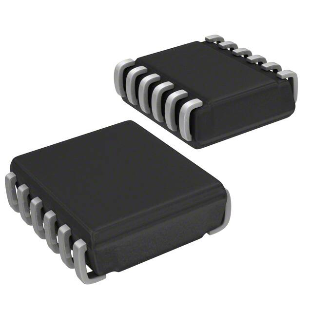
• TSOPJW-12 Package
The AAT4674-1 connects the supply voltage on IN1 to
OUT, or IN2 to OUT, through a very low RDS(ON) power
MOSFET that minimizes voltage drops and power dissipation. The enable (EN) and select (SEL) pin voltages
control the operational state of the internal power
MOSFET switches. Once enabled, the SEL pin will switch
between the IN1 and IN2 inputs. If both input voltages
are below the UVLO, then the AAT467-1 output floats. If
one of the input voltages is above the UVLO threshold
then that input voltage that is above the UVLO threshold
is passed through to the output.
The two power switches are current limited and the current limit thresholds can be programmed through the
resistors on IIN1 and IIN2 pins respectively.
Applications
•
•
•
•
•
•
Bluetooth™ Headsets
Cell Phones
Digital Still Cameras
MP3 Players
Personal Data Assistants (PDAs)
Set Top Boxes
The AAT4674-1 is available in the thermally enhanced,
space-saving Pb-free 12-pin TSOPJW package. The 46741 is specified for operation over the -40°C to +85°C
temperature range.
Typical Application
+5V
IN1
System Load
OUT
+3.3V
IN2
IN1/IN2 Select
SEL
IIN1
IIN2
RIIN2
Enable
RIIN1
EN
GND
Skyworks Solutions, Inc. • Phone [781] 376-3000 • Fax [781] 376-3100 • sales@skyworksinc.com • www.skyworksinc.com
201911A • Skyworks Proprietary Information • Products and Product Information are Subject to Change Without Notice. • April 26, 2012
1
�DATA SHEET
AAT4674
Power Supply Selector Switch
Pin Descriptions
Pin Number
Name
Type
1, 2
3, 4
5
6, 7
IN1
IN2
EN
GND
I
I
I
I/O
8
SEL
I
9
10
11, 12
IIN2
IIN1
OUT
I
I
O
Function
Power supply 1 input.
Power supply 2 input.
Enable pin, active low.
Ground.
IN2 or IN1 select input.
Logic ‘0’ OUT = IN1
Logic ‘1’ OUT = IN2
IN2-OUT switch current limit set resistor input.
IN1-OUT switch current limit set resistor input.
Output pin.
Pin Configuration
TSOPJW-12
(Top View)
IN1
IN1
IN2
IN2
EN
GND
2
1
12
2
11
3
10
4
9
5
8
6
7
OUT
OUT
IIN1
IIN2
SEL
GND
Skyworks Solutions, Inc. • Phone [781] 376-3000 • Fax [781] 376-3100 • sales@skyworksinc.com • www.skyworksinc.com
201911A • Skyworks Proprietary Information • Products and Product Information are Subject to Change Without Notice. • April 26, 2012
�DATA SHEET
AAT4674
Power Supply Selector Switch
Absolute Maximum Ratings1
Symbol
VINX
VN
TLEAD
IOUT
Description
[IN1, IN2] to GND
[OUT, EN, IIN1, IIN2, SEL] to GND
Maximum Soldering Temperature (at Leads)
Maximum Output Current
Value
Units
-0.3 to 6.5
-0.3 to VINX + 0.3
300
3
V
V
°C
A
Value
Units
160
625
-40 to 150
°C/W
mW
°C
Thermal Information2
Symbol
JA
PD
TJ
Description
Maximum Thermal Resistance
Maximum Power Dissipation
Operating Junction Temperature Range
1. Stresses above those listed in Absolute Maximum Ratings may cause permanent damage to the device. Functional operation at conditions other than the operating conditions
specified is not implied. Only one Absolute Maximum Rating should be applied at any one time.
2. Mounted on a FR4 board.
Skyworks Solutions, Inc. • Phone [781] 376-3000 • Fax [781] 376-3100 • sales@skyworksinc.com • www.skyworksinc.com
201911A • Skyworks Proprietary Information • Products and Product Information are Subject to Change Without Notice. • April 26, 2012
3
�DATA SHEET
AAT4674
Power Supply Selector Switch
Electrical Characteristics1
VINX = 5V, TA = -40 to +85°C, unless otherwise noted. Typical values are at TA = 25°C.
Symbol
Description
Conditions
Min
Operation
IN1 Operating Voltage Range
VIN1
VIN2
IN2 Operating Voltage Range
VUVLO_IN1
IN1 Under-Voltage Lockout
VUVLO_IN2
IN2 Under-Voltage Lockout
IIN1_OP
IN1 Normal Operating Current2
IIN1_SHDN
IN1 Shutdown Mode Current
IIN1_SLP
IN1 Sleep Current
IIN2_OP
IN2 Normal Operating Current2
IIN2_SHDN
IN2 Shutdown Mode Current
IN2 Sleep Current
IIN2_SLP
Power Switches
RDS(ON) IN1
IN1-to-OUT FET On-Resistance
RDS(ON) IN2
IN2-to-OUT FET On-Resistance
OUT Voltage Droop From the Lower Voltage of IN1 and
IN2, When Switching Over Between IN1 and IN2
Current Regulation
tSOFT_START Soft-Start Delay
ILIM_range
IN1/IN2 Current Limit Range
IN1/IN2 Current Limit Accuracy
ILIM_ACC
Logic Control / Protection
VIH(EN)
Logic High Threshold
VIL(EN)
Logic Low Threshold
VDROOP_OUT
TSHDN
Chip Thermal Shutdown Temperature
Typ
Max
Units
6
6
2.3
V
V
2.5
2.5
Rising edge
Hysteresis
Rising edge
Hysteresis
VIN1 = 5V, VEN = 0V
VIN1 = VEN = 5V, OUT open
VIN1 = 2.5V, VIN2 = 5V, VEN =0V
VIN2 = 5V, VEN = 0V
VIN2 = VEN = 5V, OUT open
VIN1 = 5V, VIN2 = 2.5V, VEN = 0V
VIN1
VIN1
VIN2
VIN2
=
=
=
=
5.0V,
3.5V,
5.0V,
3.5V,
TA
TA
TA
TA
=
=
=
=
0.1
2.3
0.1
10
0.12
0.14
0.12
0.14
0.15
0.18
0.15
0.18
1
10
25°C
25°C
25°C
25°C
IO(OUT) = 0.5A, CO(OUT) = 10μF
150
Delay of start from EN, or UVLO
RIIN1/IIN2 = 100k
1
30
1
5
30
1
5
1
140
15
μA
μA
μA
μA
μA
μA
2.0
1.2
μs
A
A
0.4
V
V
1.6
Threshold
Hysteresis
V
mV
100
0.2
0.8
V
°C
1. The AAT4674 is guaranteed to meet performance specifications over the -40°C to +85°C operating temperature range and is assured by design, characterization, and correlation with statistical process controls.
2. Additional operating current is required by the RIINx current limit setting resistors. The amount of current required by the RIINx resistors is the current limit divided by 1000.
Therefore IINx_OP = (0.5V/RIINx)*(200k/1000) or approximately ILIM/1000.
4
Skyworks Solutions, Inc. • Phone [781] 376-3000 • Fax [781] 376-3100 • sales@skyworksinc.com • www.skyworksinc.com
201911A • Skyworks Proprietary Information • Products and Product Information are Subject to Change Without Notice. • April 26, 2012
�DATA SHEET
AAT4674
Power Supply Selector Switch
Typical Characteristics
IIN2 Shutdown Current vs. Temperature
0.8
0.6
IIN2 Shutdown Current (µA)
IIN1 Shutdown Current (µA)
IIN1 Shutdown Current vs. Temperature
VIN1 = 6.5V
0.4
VIN1 = 5V
0.2
0
VIN1 = 3.6V
-0.2
-0.4
-40
VIN1 = 4.2V
-15
10
35
60
85
0.8
0.6
0.4
VIN2 = 6.5V
0.2
VIN2 = 5V
0
VIN2 = 3.6V
-0.2
VIN2 = 4.2V
-0.4
-40
-15
10
IIN2 Operation Current vs. Temperature
(IOUT = 0A)
(IOUT = 0A)
VIN1 = 6.5V
18
VIN1 = 5V
16
14
12
10
VIN1 = 3.6V
8
VIN1 = 4.2V
6
4
-40
-15
10
35
60
85
20
18
VIN2 = 6.5V
16
VIN2 = 5V
14
12
VIN2 = 4.2V
10
VIN2 = 3.6V
8
6
4
-40
-15
10
Temperature (°C)
60
85
Enable Threshold vs. Input Voltage
250
1.1
VIN = 3.5V
Enable Threshold (V)
RDS(ON) (mΩ)
35
Temperature (°C)
RDS(ON) vs. Temperature
VIN = 2.5V
150
100
VIN = 6.5V
VIN = 5V
50
0
85
IIN1 Operation Current vs. Temperature
20
200
60
Temperature (°C)
IIN2 Operation Current (µA)
IIN1 Operation Current (µA)
Temperature (°C)
35
-40
-15
10
35
60
Temperature (°C)
85
110
1.05
1
VIH(EN)
0.95
0.9
0.85
VIL(EN)
0.8
0.75
0.7
0.65
0.6
2.5
3
3.5
4
4.5
5
5.5
6
6.5
Input Voltage (V)
Skyworks Solutions, Inc. • Phone [781] 376-3000 • Fax [781] 376-3100 • sales@skyworksinc.com • www.skyworksinc.com
201911A • Skyworks Proprietary Information • Products and Product Information are Subject to Change Without Notice. • April 26, 2012
5
�DATA SHEET
AAT4674
Power Supply Selector Switch
Typical Characteristics
IIN1 Sleep Current vs. VIN1 Voltage
IIN2 Sleep Current vs. VIN2 Voltage
(VIN2 = 6.5V)
(VIN1 = 6.5V)
2.5
IIN2 Sleep Current (µA)
IIN1 Sleep Current (µA)
2.5
85°C
2
25°C
1.5
1
-40°C
0.5
2
85°C
25°C
1.5
1
-40°C
0.5
0
0
2.5
3
3.5
4
4.5
5
5.5
6
2.5
3
3.5
VIN1 Voltage (V)
4
4.5
5
5.5
VIN2 Voltage (V)
Current Limit vs. RIIN1/IIN2
Turn-On/Off Response
(ROUT = 10Ω
Ω; VIN = 5V)
(VIN1 = 5V; VIN2 = 3.3V; VOUT = VIN2 or VOUT = VIN1)
2.25
Current Limit (A)
2
VEN
(2V/div)
1.75
2V
0V
1.5
1.25
1
0.75
VOUT
(5V/div)
0V
IOUT
(500mA/div)
0A
0.5
0.25
0
50
100
150
200
250
300
350
400
450
500
Ω)
RIIN1/IIN2 (kΩ
3.3V to 5V Transition Response
5V to 3.3V Transition Response
(IOUT = 500mA, COUT = 10µF)
(IOUT = 500mA, COUT = 10µF)
5V
VOUT
(1V/div)
VSEL
(2V/div)
VOUT
(1V/div)
5V
3.3V
3.3V
2V
0V
Time (40µs/div)
6
Time (100µs/div)
VSEL
(2V/div)
2V
0V
Time (40µs/div)
Skyworks Solutions, Inc. • Phone [781] 376-3000 • Fax [781] 376-3100 • sales@skyworksinc.com • www.skyworksinc.com
201911A • Skyworks Proprietary Information • Products and Product Information are Subject to Change Without Notice. • April 26, 2012
6
�DATA SHEET
AAT4674
Power Supply Selector Switch
Typical Characteristics
3.6V to 3.6V Transition Response
Short Circuit Through 0.3Ω
Ω Response
(IOUT = 500mA, COUT = 10µF)
VOUT
(1V/div)
VSEL
(2V/div)
3.6V
VIN
(2V/div)
5V
IOUT
(5A/div)
0A
3.6V
VOUT
(5V/div)
2V
0V
2A
5V
0.6V
Time (40µs/div)
Time (10µs/div)
Short Circuit Through 0.6Ω
Ω Response
Thermal Shutdown Response
(VIN = 5V)
VIN
(2V/div)
IOUT
(5A/div)
VOUT
(5V/div)
5V
VEN
(2V/div)
0A
5V
Time (10µs/div)
2A
VOUT
(2V/div)
1.2V
IOUT
(2A/div)
2V
0V
0V
0A
Time (40ms/div)
Skyworks Solutions, Inc. • Phone [781] 376-3000 • Fax [781] 376-3100 • sales@skyworksinc.com • www.skyworksinc.com
201911A • Skyworks Proprietary Information • Products and Product Information are Subject to Change Without Notice. • April 26, 2012
7
�DATA SHEET
AAT4674
Power Supply Selector Switch
Functional Block Diagram
Switch 1
IN1
OUT
IIN1
Thermal
and Current
Sense
SEL
Logic
Control
EN
IIN2
GND
IN2
Switch 2
Truth Table
Y = Yes, N = No, X = don’t care.
Input Conditions
VIN1 > UVLO
VIN2 > UVLO
SEL
AAT4674-1
VOUT
N
Y
N
Y
Y
N
N
Y
Y
Y
X
X
X
0
1
Floating
VIN1
VIN2
VIN1
VIN2
Functional Description
To power the output, both input supplies (IN1 and IN2)
must be above the UVLO threshold. If either supply input
is below the UVLO threshold then the output of the
AAT4674-1 will be the input supply that is above the
UVLO threshold. If both supplies are above the UVLO
threshold and the device is enabled, the AAT4674-1 will
connect the supply from IN1 to OUT when the SEL pin is
LOW (logic ‘0’), and when the SEL pin is HIGH (logic ‘1’)
then the supply on IN2 is connected to the OUT pin.
Consult the above “Truth Table” for the summarized
AA4674-1 operational details.
The two internal power switches are current limited and
the limiting thresholds can be programmed through the
resistors on the IIN1 and IIN2 pins respectively.
8
Applications Information
Input Capacitors
A 1μF or greater capacitor is generally recommended
between IN1 and GND (CIN1), and between IN2 and GND
(CIN2). An input capacitor is not required for basic operation; however, it is useful in preventing load transients
from affecting up-stream circuits. Ceramic, tantalum, or
aluminum electrolytic capacitors may be selected for CIN1/
CIN2. There is no specific capacitor equivalent series resistance (ESR) requirement for CIN1/CIN2. However, for higher
current operation, ceramic capacitors are recommended
for CIN1/CIN2 due to their inherent capability over tantalum
capacitors to withstand input current surges from low
impedance sources such as batteries in portable devices.
Skyworks Solutions, Inc. • Phone [781] 376-3000 • Fax [781] 376-3100 • sales@skyworksinc.com • www.skyworksinc.com
201911A • Skyworks Proprietary Information • Products and Product Information are Subject to Change Without Notice. • April 26, 2012
�DATA SHEET
AAT4674
Power Supply Selector Switch
Output Capacitor
A 1μF or greater capacitor is required between OUT and
GND (COUT). As with the input capacitor, there is no specific capacitor ESR requirement. If desired, COUT may be
increased to accommodate any load transient condition.
EN Input
For IN2 (power supply 2 input):
⎛ VIIN2 ⎞
RIIN2 = ⎝ I
⎠ · 200k
CLIN2
⎛0.5V⎞
= ⎝0.2A⎠ · 200k
= 500kΩ (499.9kΩ standard value)
The AAT4674-1 is enabled when VEN is ≤ 0.4V (logic ‘0’),
conversely the AAT4674-1 is disabled when VEN is ≥ 1.6V
(logic ‘1’).
SEL Input
When VSEL is ≤ 0.4V (logic ‘0’) the output voltage equals
power supply 1 input (VOUT = VIN1), and conversely when
VSEL is ≥ 1.6V (logic ‘1’) the output voltage equals power
supply 2 input (VOUT = VIN2).
Current Limit Resistor Selection
The current limits for power supply 1 and power supply 2
inputs are set by resistors connected between IIN1/IIN2
and GND. The following equation can be used to select
the appropriate resistor for a particular current limit:
⎛VIINX ⎞
ICLINX = ⎝R ⎠ · 200k
IINX
ICLINX Current limit for IN1 and/or IN2 pins respectively
VIINX Internally Regulated Voltage [0.5V ± 20%] on the
IIN1 and IIN2 pins respectively
RIINX IIN1 and/or IIN2 Resistor
200k Internal Gain Factor
Design Example
A particular application requires that the current limit for
IN1 be set to 2A and the current limit for IN2 be set to
0.2A. What value of resistor is required for the IIN1 and
IIN2 pins respectively?
For IN1 (power supply 1 input):
⎛ VIIN1 ⎞
RIIN1 = ⎝ I
⎠ · 200k
CLIN1
⎛0.5V⎞
= ⎝ 2A ⎠ · 200k
= 50kΩ (49.9kΩ standard value)
Thermal Considerations
Since the AAT4674-1 has an internal current limit and
over-temperature protection (thermal shutdown), junction temperature is rarely a concern. However, if the
application requires large currents in a high temperature
environment, it is possible that temperature rather than
current limit will be the dominant regulating condition. In
these applications, the maximum current available without risk of an over-temperature condition must be calculated. The maximum internal temperature while current
limit is not active can be calculated using Equation 1.
Eq. 1: TJ(MAX) = IMAX2 · RDS(ON)(MAX) · RθJA + TA(MAX)
In Equation 1, IMAX is the maximum current required by
the load. RDS(ON)(MAX) is the maximum rated RDS(ON) of the
AAT4674-1 at high temperatures (consult the “RDSON vs.
Temperature” performance graph in the “Typical
Characteristics” section of this datasheet). For estimating the RDS(ON)(MAX) use the data on the “RDSON vs
Temperature” performance graph and increase the value
from the performance graph by 50%. RθJA is the thermal
resistance between the AAT4674-1 and the printed circuit board (PCB) onto which it is mounted; RJA is the
thermal resistance of the TSOPJW-12 package. TA(MAX) is
the maximum ambient temperature that the PCB under
the AAT4674-1 would be if the AAT4674-1 were not dissipating power. Equation 1 can be rearranged to solve for
IMAX, into Equation 2.
Eq. 2: IMAX =
TSD(MIN) - TA(MAX)
RDS(ON)(MAX) · RΘJA
TSD(MIN) is the minimum temperature required to activate
the AAT4674-1 over-temperature protection (thermal
shutdown). With typical specification of 140°C, 125°C is
a safe minimum value to use.
Skyworks Solutions, Inc. • Phone [781] 376-3000 • Fax [781] 376-3100 • sales@skyworksinc.com • www.skyworksinc.com
201911A • Skyworks Proprietary Information • Products and Product Information are Subject to Change Without Notice. • April 26, 2012
9
�DATA SHEET
AAT4674
Power Supply Selector Switch
For example, for a 2.5V input power supply application
that is specified to operate in 50°C environments where
the PCB operates at temperatures as high as 85°C. The
application is sealed and its PCB is small, causing RθJA to
be approximately 160°C/W. The RDS(ON)(MAX) is estimate to
be 300mΩ (from the “RDS(ON) vs. Temperature” performance graph, where VIN = 2.5V at 85°C plus 50%). To
find the maximum current (IMAX) for this application use
Equation 2:
IMAX =
10
125°C - 85°C
300mΩ · 160°C/W = 0.913A
PCB Layout Recommendations
For proper thermal management, to minimize PCB trace
resistance, and to take advantage of the low RDS(ON) values of the two internal power switches in the AAT46741, certain circuit board layout rules should be followed:
IN1, IN2, and OUT should be routed using wider than
normal traces. The two IN1 pins (1 and 2) and two IN2
pins (3 and 4) should be connected to the same wide
PCB trace; and GND should be connected to a ground
plane. For best performance, the input capacitors (CIN1/
CIN2) and output capacitors (COUT) should be placed as
close to the package pins as possible. The AAT4674-1
evaluation board layout follows the printed circuit board
layout recommendations and can be used as an example
of an optimal board layout.
Skyworks Solutions, Inc. • Phone [781] 376-3000 • Fax [781] 376-3100 • sales@skyworksinc.com • www.skyworksinc.com
201911A • Skyworks Proprietary Information • Products and Product Information are Subject to Change Without Notice. • April 26, 2012
�DATA SHEET
AAT4674
Power Supply Selector Switch
Evaluation Board Schematic
C1
2.2μF
OUT
MAIN
U1
1
2
AUX
3
4
5
C2
2.2μF
6
IN1
IN1
IN2
IN2
EN
GND
OUT
OUT
IIN1
IIN2
SEL
GND
12
11
10
9
2
1
7
R3
49.9K R2
49.9K
GND
Header 2
EN
R1
100K
IMAIN
IAUX
8
AAT4674-1
J1
C3
2.2μF
PWRSEL
Figure 1: AAT4674-1 Evaluation Board Schematic.
Evaluation Board Layout
Figure 2: AAT4674-1 Evaluation
Board Top Side Layout.
Figure 3: AAT4674-1 Evaluation
Board Bottom Side Layout.
Skyworks Solutions, Inc. • Phone [781] 376-3000 • Fax [781] 376-3100 • sales@skyworksinc.com • www.skyworksinc.com
201911A • Skyworks Proprietary Information • Products and Product Information are Subject to Change Without Notice. • April 26, 2012
11
�DATA SHEET
AAT4674
Power Supply Selector Switch
Ordering Information
Package
Marking1
Part Number (Tape and Reel)2
TSOPJW-12
YTXYY
AAT4674ITP-1-T1
Skyworks Green™ products are compliant with
all applicable legislation and are halogen-free.
For additional information, refer to Skyworks
Definition of Green™, document number
SQ04-0074.
Package Information
TSOPJW-12
2.85 ± 0.20
2.40 ± 0.10
0.20 + 0.10
- 0.05
0.50 BSC 0.50 BSC 0.50 BSC 0.50 BSC 0.50 BSC
7° NOM
0.04 REF
0.055 ± 0.045
0.15 ± 0.05
+ 0.10
1.00 - 0.065
0.9625 ± 0.0375
3.00 ± 0.10
4° ± 4°
0.45 ± 0.15
0.010
2.75 ± 0.25
All dimensions in millimeters.
1. XYY = assembly and date code.
2. Sample stock is generally held on part numbers listed in BOLD.
Copyright © 2012 Skyworks Solutions, Inc. All Rights Reserved.
Information in this document is provided in connection with Skyworks Solutions, Inc. (“Skyworks”) products or services. These materials, including the information contained herein, are provided by Skyworks as a
service to its customers and may be used for informational purposes only by the customer. Skyworks assumes no responsibility for errors or omissions in these materials or the information contained herein. Skyworks may change its documentation, products, services, specifications or product descriptions at any time, without notice. Skyworks makes no commitment to update the materials or information and shall have no
responsibility whatsoever for conflicts, incompatibilities, or other difficulties arising from any future changes.
No license, whether express, implied, by estoppel or otherwise, is granted to any intellectual property rights by this document. Skyworks assumes no liability for any materials, products or information provided hereunder, including the sale, distribution, reproduction or use of Skyworks products, information or materials, except as may be provided in Skyworks Terms and Conditions of Sale.
THE MATERIALS, PRODUCTS AND INFORMATION ARE PROVIDED “AS IS” WITHOUT WARRANTY OF ANY KIND, WHETHER EXPRESS, IMPLIED, STATUTORY, OR OTHERWISE, INCLUDING FITNESS FOR A PARTICULAR
PURPOSE OR USE, MERCHANTABILITY, PERFORMANCE, QUALITY OR NON-INFRINGEMENT OF ANY INTELLECTUAL PROPERTY RIGHT; ALL SUCH WARRANTIES ARE HEREBY EXPRESSLY DISCLAIMED. SKYWORKS DOES
NOT WARRANT THE ACCURACY OR COMPLETENESS OF THE INFORMATION, TEXT, GRAPHICS OR OTHER ITEMS CONTAINED WITHIN THESE MATERIALS. SKYWORKS SHALL NOT BE LIABLE FOR ANY DAMAGES, INCLUDING BUT NOT LIMITED TO ANY SPECIAL, INDIRECT, INCIDENTAL, STATUTORY, OR CONSEQUENTIAL DAMAGES, INCLUDING WITHOUT LIMITATION, LOST REVENUES OR LOST PROFITS THAT MAY RESULT FROM
THE USE OF THE MATERIALS OR INFORMATION, WHETHER OR NOT THE RECIPIENT OF MATERIALS HAS BEEN ADVISED OF THE POSSIBILITY OF SUCH DAMAGE.
Skyworks products are not intended for use in medical, lifesaving or life-sustaining applications, or other equipment in which the failure of the Skyworks products could lead to personal injury, death, physical or environmental damage. Skyworks customers using or selling Skyworks products for use in such applications do so at their own risk and agree to fully indemnify Skyworks for any damages resulting from such improper
use or sale.
Customers are responsible for their products and applications using Skyworks products, which may deviate from published specifications as a result of design defects, errors, or operation of products outside of published parameters or design specifications. Customers should include design and operating safeguards to minimize these and other risks. Skyworks assumes no liability for applications assistance, customer product
design, or damage to any equipment resulting from the use of Skyworks products outside of stated published specifications or parameters.
Skyworks, the Skyworks symbol, and “Breakthrough Simplicity” are trademarks or registered trademarks of Skyworks Solutions, Inc., in the United States and other countries. Third-party brands and names are for
identification purposes only, and are the property of their respective owners. Additional information, including relevant terms and conditions, posted at www.skyworksinc.com, are incorporated by reference.
12
Skyworks Solutions, Inc. • Phone [781] 376-3000 • Fax [781] 376-3100 • sales@skyworksinc.com • www.skyworksinc.com
201911A • Skyworks Proprietary Information • Products and Product Information are Subject to Change Without Notice. • April 26, 2012
�


 工商网监
湘ICP备2023018690号
工商网监
湘ICP备2023018690号