DATA SHEET
ATN3590 Series: Fixed Attenuators
Applications
Level adjustment in radios, radars, EW/ECM equipment, and test instruments
Features
Fixed value, absorptive devices Available attenuation values range from 0 to 10 dB (in 1 dB steps), and 12, 15, 20, and 30 dB Suitable for use to 40 GHz or higher Excellent return loss: 30 dB, typical Enhanced power handling: 2 W
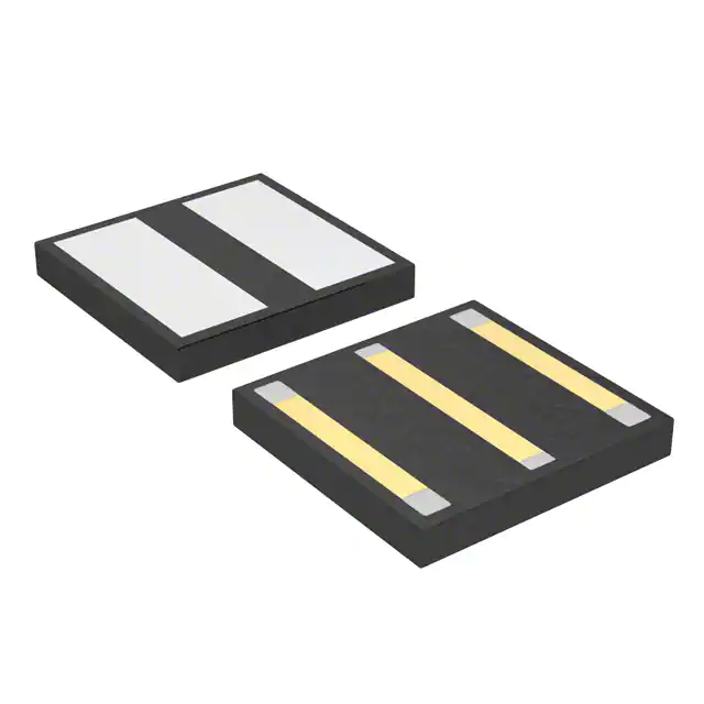
Back Side
Out
Back Side
Skyworks offers lead (Pb)-free, RoHS (Restriction of Hazardous Substances) compliant packaging.
In Schematic
Figure 1. Typical Attenuator Die and Circuit
Description
The ATN3590 family of fixed resistive attenuators are integrated circuits comprising thin film resistors and through-die vias that provide excellent attenuation flatness from low frequency to 40 GHz or higher. These attenuators are available from 0 to 30 dB (see Table 2). The ATN3590 attenuator family is optimized for surface mounting on co-planar waveguide or microstrip printed circuit boards. Bond wires or ribbons are used to connect the input and output ports of the attenuators to the external circuit transmission lines. Connection to ground is accomplished by through-die vias to the die backside metallization. The dice are attached using eutectic solder or conductive epoxy and can operate over a temperature range of –65 C to 150 C. The absolute maximum ratings for the ATN3590 attenuators are provided in Table 1 and the electrical specifications are shown in Table 2. Typical performance characteristics are illustrated in Figures 2 through 8.
Skyworks Solutions, Inc. • Phone [781] 376-3000 • Fax [781] 376-3100 • sales@skyworksinc.com • www.skyworksinc.com
200842B • Skyworks Proprietary Information • Products and Product Information are Subject to Change Without Notice • December 2, 2009 1
�DATA SHEET • ATN3590 SERIES FIXED ATTENUATORS
Table 1. ATN3590 Series Absolute Maximum Ratings
Parameter Input power Power dissipation @ 25 °C Operating temperature Storage temperature
Note:
Symbol PIN PDIS TOP TSTG
Minimum
Typical
Maximum 2 2
Units W W C C
–55 –55
+150 +150
Exposure to maximum rating conditions for extended periods may reduce device reliability. There is no damage to device with only one parameter set at the limit and all other parameters set at or below their nominal value. Exceeding any of the limits listed here may result in permanent damage to the device.
CAUTION: Although this device is designed to be as robust as possible, Electrostatic Discharge (ESD) can damage this device. This device must be protected at all times from ESD. Static charges may easily produce potentials of several kilovolts on the human body or equipment, which can discharge without detection. Industry-standard ESD precautions should be used at all times.
Table 2. ATN3590Series Electrical Specifications (Note 1) (TOP = +25 C, Characteristic Impedance [ZO] = 50 Ω, Unless Otherwise Noted)
Attenuation Attenuation Attenuation Attenuation Min. Return Min. Return Min. Return Min. Return Attenuation Flatness Flatness Flatness Flatness Loss Loss Loss Loss Attenuation Tolerance (Note 2) (Note 2) (Note 2) (Note 2) DC–12 GHz 12–26 GHz 26–33 GHz 33–40 GHz @ DC (dB) DC–12 GHz 12–26 GHz 26–33 GHz 33–40 GHz (dB) (dB) (dB) (dB) (dB) (dB) (dB) (dB) (dB) 0 1 2 3 4 5 6 7 8 9 10 12 15 20 30 0.25 ±0.20 ±0.20 ±0.20 ±0.20 ±0.20 ±0.40 ±0.40 ±0.40 ±0.40 ±0.40 ±0.40 ±0.40 ±1.0 ±1.0 ±0.15 ±0.15 ±0.15 ±0.15 ±0.15 ±0.15 ±0.15 ±0.15 ±0.15 ±0.20 ±0.20 ±0.20 ±0.20 ±0.20 ±0.20 ±0.15 ±0.15 ±0.15 ±0.15 ±0.15 ±0.15 ±0.15 ±0.15 ±0.15 ±0.20 ±0.20 ±0.20 ±0.20 ±0.20 ±0.25 ±0.20 ±0.20 ±0.20 ±0.20 ±0.20 ±0.20 ±0.20 ±0.20 ±0.20 ±0.25 ±0.25 ±0.30 ±0.50 ±0.75 ±0.75 ±0.20 ±0.20 ±0.20 ±0.20 ±0.20 ±0.20 ±0.20 ±0.20 ±0.20 ±0.30 ±0.50 ±0.50 ±0.75 ±1.00 ±2.50 28 28 28 28 28 28 28 28 28 28 28 28 28 28 28 24 24 24 24 24 24 24 24 24 24 24 24 24 24 24 20 20 20 20 20 20 20 20 20 20 20 20 20 20 20 16 16 16 16 16 16 16 16 16 16 16 16 16 16 16
Part Number
ATN3590-00 ATN3590-01 ATN3590-02 ATN3590-03 ATN3590-04 ATN3590-05 ATN3590-06 ATN3590-07 ATN3590-08 ATN3590-09 ATN3590-10 ATN3590-12 ATN3590-15 ATN3590-20 ATN3590-30
Note 1: Performance is guaranteed only under the conditions listed in this Table. Note 2: Flatness is defined as the maximum deviation from the mean value of attenuation over the specified frequency range.
Skyworks Solutions, Inc. • Phone [781] 376-3000 • Fax [781] 376-3100 • sales@skyworksinc.com • www.skyworksinc.com
2 December 2, 2009 • Skyworks Proprietary Information • Products and Product Information are Subject to Change Without Notice • 200842B
�DATA SHEET • ATN3590 SERIES FIXED ATTENUATORS
Typical Performance Characteristics
(TOP = +25 C, Characteristic Impedance [ZO] = 50 Ω, Unless Otherwise Noted. Data Gathered Using Ground-to-Signal-to-Ground Probes on Die)
+2.0 +1.5 +1.0 +0.5
–2.0
0 dB 1 dB 2 dB
Attenuation (dB)
–2.5 –3.0 –3.5 –4.0 –4.5 –5.0 –5.5
3 dB 4 dB 5 dB
Attenuation (dB)
0
–0.5 –1.0 –1.5 –2.0 –2.5 –3.0 –3.5 –4.0 0 5 10 15 20 25 30 35 40
–6.0 0 5 10 15 20 25 30 35 40
Frequency (GHz)
Frequency (GHz)
Figure 2. Attenuation vs Frequency (0 dB, 1 dB, and 2 dB Attenuators)
–5.0 –5.5 –6.0 –6.5 –7.0 –7.5 –8.0 –8.5 –9.0
Figure 3. Attenuation vs Frequency (3 dB, 4 dB, and 5 dB Attenuators)
–8
6 dB 7 dB 8 dB
–9
Attenuation (dB)
Attenuation (dB)
–10
–11
–12
–13
9 dB 10 dB 12 dB
0 5 10 15 20 25 30 35 40
0
5
10
15
20
25
30
35
40
–14
Frequency (GHz)
Frequency (GHz)
Figure 4. Attenuation vs Frequency (6 dB, 7 dB, and 8 dB Attenuators)
–14 –16 –18
Figure 5. Attenuation vs Frequency (9 dB, 10 dB, and 12 dB Attenuators)
Attenuation (dB)
–20 –22 –24 –26 –28 –30 –32 0 5 10 15 20 25 30 35 40
15 dB 20 dB 30 dB
Frequency (GHz)
Figure 6. Attenuation vs Frequency (15 dB, 20 dB, and 30 dB Attenuators)
Skyworks Solutions, Inc. • Phone [781] 376-3000 • Fax [781] 376-3100 • sales@skyworksinc.com • www.skyworksinc.com
200842B • Skyworks Proprietary Information • Products and Product Information are Subject to Change Without Notice • December 2, 2009 3
�DATA SHEET • ATN3590 SERIES FIXED ATTENUATORS
0 –10 –20
0
0 dB 6 dB 15 dB
1 dB 7 dB 20 dB
2 dB 8 dB 30 dB
3 dB 9 dB
4 dB 10 dB
5 dB 12 dB
–10 –20
0 dB 6 dB 15 dB
1 dB 7 dB 20 dB
2 dB 8 dB 30 dB
3 dB 9 dB
4 dB 10 dB
5 dB 12 dB
Input Return Loss (dB)
Small Signal Gain (dB)
–30 –40 –50 –60 –70 –80
–30 –40 –50 –60 –70 –80
0
5
10
15
20
25
30
35
40
0
5
10
15
20
25
30
35
40
Frequency (GHz)
Frequency (GHz)
Figure 7. Input Return Loss vs Frequency
Figure 8. Small Signal Gain vs Frequency
Technical Description
The ATN3590 family of fixed attenuators comprises devices with nominal attenuation values of 0 to 10 dB (in 1 dB steps), and 12, 15, 20, and 30 dB. These attenuators contain through-wafer vias that connect the topside ground to the backside metallization of each die. The devices with nominal attenuation values of 1 dB or greater are fabricated using thin film resistors deposited on high resistivity silicon substrates. The circuit topology is a simple tee structure that consists of two series resistors and a shunt resistance, which in this case is realized as a pair of shunt resistors connected to the node between the two series resistors (refer to Figures 9 and 10). The resistances of each of these resistors are selected to simultaneously produce the nominal attenuation with very good input and output return losses. The attenuators with nominal attenuation values ≥6 dB contain a pair of cascaded tee sections (see Figure 11). The 0 dB attenuator, ATN3590-00, is a 50 Ω microstrip transmission line with identical foot print and bond pads to those of the other products in this family.
R3 R1 R4 R2
Figure 9. Circuit Topology (1 – 5 dB Attenuators)
R1
R4
R2 || R3
Figure 10. Simplified Circuit Topology (1 – 5 dB Attenuators)
Die Attachment and Signal Path Connection
Any of the ATN3590 family of attenuators should be mounted on the ground plane of a transmission medium. The die should be attached with conductive epoxy or a eutectic solder such as gold/tin (AuSn). For good high frequency performance, it is essential that there is no ground plane directly beneath the series signal path of the ATN3590. The backside metallization on the die is split into two regions along the sides of the die to accommodate this requirement.
R3 R1 R4 R2 R6 R7 R5
Figure 11. Circuit Topology for Attenuators with Nominal Attenuation ≥6 dB
Skyworks Solutions, Inc. • Phone [781] 376-3000 • Fax [781] 376-3100 • sales@skyworksinc.com • www.skyworksinc.com
4 December 2, 2009 • Skyworks Proprietary Information • Products and Product Information are Subject to Change Without Notice • 200842B
�DATA SHEET • ATN3590 SERIES FIXED ATTENUATORS
The metallization on the circuit medium to which the attenuator is to be mounted must also include the split in the ground connections. It is recommended that the gap between the ground pads on the circuit medium should be 250 μm wide by 900 μm long. The input and output signal paths should be connected to the signal path bond pads on the attenuator with Au ribbons or wires. It is recommended that these connections be made with 0.25 x 3 mil (6.25 x 75 microns) ribbons, as shown in Figure 12.
Package Dimensions
The PCB layout footprint for the ATN3590 attenuators is shown in Figure 13. Package dimensions are provided in Figure 14.
Packaging
The standard mode of packaging for shipment of the ATN3590 Attenuator Series is 100 pieces per GelPak™.
0.25 x 3 mil Au Ribbon (2 Places)
Ground
Input/Output
Output/Input
Ground
Figure 12. Suggested Die Mount and Ribbon Attachment
For best performance, no PCB topside ground metal should remain in this area (250 x 900 microns, centered on die)
Figure 13. PCB Layout Footprint
Ground metal (2 places)
Skyworks Solutions, Inc. • Phone [781] 376-3000 • Fax [781] 376-3100 • sales@skyworksinc.com • www.skyworksinc.com
200842B • Skyworks Proprietary Information • Products and Product Information are Subject to Change Without Notice • December 2, 2009 5
�DATA SHEET • ATN3590 SERIES FIXED ATTENUATORS
0.725 Additional Ground Contacts 0.110 x 0.075 (4 Places)
10DB
0.700
Attenuator Value Ground Via to Backside (8 Places) Input/Output Pad 0.110 x 0.075 (2 Places)
Low Inductance Ground Contact (Cu-Ti/V-Au). Solder or Conductive Epoxy Attach. 0.152
0.100
Out
Back Side
Back Side
In Schematic
Notes: 1. Resistor Configuration on Top Side of Die Varies by Attenuation Value of Device. 2. All measurements in millimeters 3. All dimensions ± 0.025 mm
S1603
Figure 14. ATN3590 Attenuator Series Die Dimensions
Copyright © 2009 Skyworks Solutions, Inc. All Rights Reserved. Information in this document is provided in connection with Skyworks Solutions, Inc. (“Skyworks”) products or services. These materials, including the information contained herein, are provided by Skyworks as a service to its customers and may be used for informational purposes only by the customer. Skyworks assumes no responsibility for errors or omissions in these materials or the information contained herein. Skyworks may change its documentation, products, services, specifications or product descriptions at any time, without notice. Skyworks makes no commitment to update the materials or information and shall have no responsibility whatsoever for conflicts, incompatibilities, or other difficulties arising from any future changes. No license, whether express, implied, by estoppel or otherwise, is granted to any intellectual property rights by this document. Skyworks assumes no liability for any materials, products or information provided hereunder, including the sale, distribution, reproduction or use of Skyworks products, information or materials, except as may be provided in Skyworks Terms and Conditions of Sale. THE MATERIALS, PRODUCTS AND INFORMATION ARE PROVIDED “AS IS” WITHOUT WARRANTY OF ANY KIND, WHETHER EXPRESS, IMPLIED, STATUTORY, OR OTHERWISE, INCLUDING FITNESS FOR A PARTICULAR PURPOSE OR USE, MERCHANTABILITY, PERFORMANCE, QUALITY OR NON-INFRINGEMENT OF ANY INTELLECTUAL PROPERTY RIGHT; ALL SUCH WARRANTIES ARE HEREBY EXPRESSLY DISCLAIMED. SKYWORKS DOES NOT WARRANT THE ACCURACY OR COMPLETENESS OF THE INFORMATION, TEXT, GRAPHICS OR OTHER ITEMS CONTAINED WITHIN THESE MATERIALS. SKYWORKS SHALL NOT BE LIABLE FOR ANY DAMAGES, INCLUDING BUT NOT LIMITED TO ANY SPECIAL, INDIRECT, INCIDENTAL, STATUTORY, OR CONSEQUENTIAL DAMAGES, INCLUDING WITHOUT LIMITATION, LOST REVENUES OR LOST PROFITS THAT MAY RESULT FROM THE USE OF THE MATERIALS OR INFORMATION, WHETHER OR NOT THE RECIPIENT OF MATERIALS HAS BEEN ADVISED OF THE POSSIBILITY OF SUCH DAMAGE. Skyworks products are not intended for use in medical, lifesaving or life-sustaining applications, or other equipment in which the failure of the Skyworks products could lead to personal injury, death, physical or environmental damage. Skyworks customers using or selling Skyworks products for use in such applications do so at their own risk and agree to fully indemnify Skyworks for any damages resulting from such improper use or sale. Customers are responsible for their products and applications using Skyworks products, which may deviate from published specifications as a result of design defects, errors, or operation of products outside of published parameters or design specifications. Customers should include design and operating safeguards to minimize these and other risks. Skyworks assumes no liability for applications assistance, customer product design, or damage to any equipment resulting from the use of Skyworks products outside of stated published specifications or parameters. Skyworks, the Skyworks symbol, and “Breakthrough Simplicity” are trademarks or registered trademarks of Skyworks Solutions, Inc., in the United States and other countries. Third-party brands and names are for identification purposes only, and are the property of their respective owners. Additional information, including relevant terms and conditions, posted at www.skyworksinc.com, are incorporated by reference.
Skyworks Solutions, Inc. • Phone [781] 376-3000 • Fax [781] 376-3100 • sales@skyworksinc.com • www.skyworksinc.com
6 December 2, 2009 • Skyworks Proprietary Information • Products and Product Information are Subject to Change Without Notice • 200842B
�