RFX1010
Production Data Sheet
700 / 800 / 900MHZ 0.5 WATT BROADBAND CMOS RFEIC
GND
17
MODE VDD1
16
15
RX
14
VDD2
13
Description
1
RXEN
12
DNC
2
TXEN
11
DNC
3
TX
10
IND
4
GND
9
ANT
5
6
DET
DNC
7
VDD3
8
GND
The RFX1010 is a broadband, fully integrated, single-chip, single-die
RFeIC (RF Front-end Integrated Circuit) which incorporates all the RF
functionality needed for a TDD-mode RF front-end operated in the
700/800/900MHz frequency bands.
The RFX1010 architecture integrates a linear PA, LNA, Transmit and
Receive switching circuitry, associated matching networks, and
harmonic filters all in a CMOS single-chip device. The RFX1010
requires minimal external components including the power supply
bypass capacitors.
This RFeIC is designed for medium to high output power, and
consumes low current in receive mode. The combination of superior
output power, high sensitivity and efficiency, low noise, small form
factor and low cost makes RFX1010 the ideal solution for multiple
applications including IEEE 802.15.4, ZigBee, AMR, Smart Home Area
Network and other ISM applications in the sub-GHz bands from 780 to
960MHz. It can also be used for IEEE 802.11p and 802.11ah.
Features
700/800/900MHz Single-Chip, Single-Die RF FrontEnd IC
Very Low DC Power Consumption
Full On-chip Matching and Decoupling Circuitry
Separate TX and RX RF Transceiver Ports and
Single Antenna Port
Minimal External Components Required
700/800/900MHz Power Amplifier with Low-Pass
Harmonic Filters
50-Ohm Input / Output Matching
Market Proven Low Cost CMOS Technology
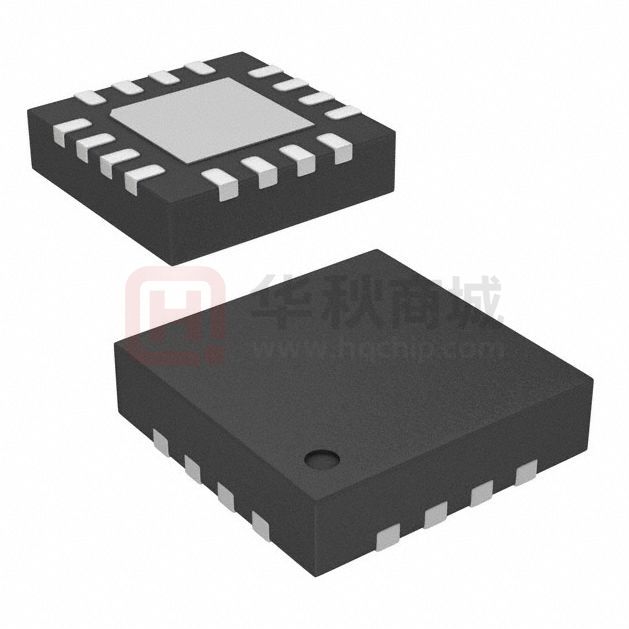
3 x 3 x 0.55mm Small Outline QFN-16 Package with
Exposed Ground Pad
Low Noise Amplifier
Transmit/Receive Switch Circuitry
High Transmit Signal Linearity Meeting Standards for
OQPSK Modulation
Low Voltage (1.2V) CMOS Control Logic
ESD Protection Circuitry on All Pins DC Grounded
RF Ports
Applications
N. America 900MHz ISM Systems
E Europe 870MHz SRD Systems
Smart Grid/AMR/AMI
Internal RF Decoupling on All VDD Bias Pins
Smart Home Appliances
Low Noise Figure for the Receive Channel
Remote Sensor and Control
High Power Handling Capability for Received Signals
Other 700/800/900MHz Radios
1
Skyworks Solutions, Inc. • Phone [781] 376-3000 • Fax [781] 376-3100 • sales@skyworksinc.com • www.skyworksinc.com
�RFX1010
Production Data Sheet
PIN ASSIGNMENTS:
Pin Number
Pin Name
Description
1
RXEN
CMOS Input to Enable Receive Mode
2
TXEN
CMOS Input to Enable Transmit Mode
3
TX
RF TX Signal from the Transceiver to the PA: DC Shorted to GND
5
DET
Analog Voltage Proportional to the PA Power Output
4, 8, 17
GND
Ground – Must Be Connected to Ground in the Application Circuit
7
VDD3
Voltage Supply Connection for the Power Stage of PA
9
ANT
Common RF Port Connected to the Antenna, DC Shorted to GND
10
IND
Port for Connecting ANT Matching Inductor
6, 11, 12
DNC
Do Not Connect – Must be left floating in the Application Circuit
13
VDD2
Voltage Supply Connection for the LNA
14
RX
RF RX Signal from the LNA to the Transceiver, DC Shorted to GND
15
VDD1
Voltage Supply Connection for the Driver Stage of PA
16
MODE
CMOS Input to Control High Gain/Low Gain for RX
PIN-OUT DIAGRAM:
RXEN
1
TXEN
2
TX
GND
MODE
VDD1
RX
VDD2
16
15
14
13
12
17
GND
DNC
11
DNC
3
10
IND
4
9
ANT
5
6
7
8
DET
DNC
VDD3
GND
(Top View)
2
Skyworks Solutions, Inc. • Phone [781] 376-3000 • Fax [781] 376-3100 • sales@skyworksinc.com • www.skyworksinc.com
�RFX1010
Production Data Sheet
ABSOLUTE MAXIMUM RATINGS:
Parameters
Units
Min
Max
Conditions
DC VDD Voltage Supply
V
0
4.2
All VDD Pins
DC Control Pin Voltage
V
0
3.6
TX RF Input Power
dBm
+7
ANT RF Input Power
dBm
+5
Junction Temperature
o
C
Storage Ambient Temperature
o
C
When RX is “ON”
+150
-50
+150
No RF and DC Voltages Applied
Appropriate care required according to
JEDEC Standards
Note: Sustained operation at or above the Absolute Maximum Ratings for any one or combinations of the above parameters may
result in permanent damage to the device and is not recommended. All Maximum RF Input Power Ratings assume 50-Ohm
terminal impedance.
RECOMENDED OPERATING CONDITIONS:
Parameters
Units
Min
Typ
Max
Conditions
DC VDD Voltage Supply (Note 1)
V
2.7
3.3
3.6
All VDD Pins
Control Voltage “High”
V
1.2
VDD
RXEN, TXEN, and MODE Pins
0.3
RXEN, TXEN, and MODE Pins
Control Voltage “Low”
V
o
Operating Ambient Temperature
ja
o
C
-40
+125
See note 2
C/W
38
Note 1 – For normal operation of the RFX1010, VDD must be continuously applied to all VDD supply pins.
Note2 – For operation above +85 oC, use the ja as guidance for system design to assure the junction
temperature will not exceed the maximum of +150 oC.
DC Characteristics (VDD=3.3V; T=+25 oC)
Parameters
Units
Min
Typ
DC Control Pin Current
Consumption
μA
0.1
DC Shutdown Current
μA
1
Max
Conditions
RXEN, TXEN, and MODE Pins
Transmit-Receive Switching Time
usec
1
Shut-Down and “ON” State
Switching Time
usec
1
3
Skyworks Solutions, Inc. • Phone [781] 376-3000 • Fax [781] 376-3100 • sales@skyworksinc.com • www.skyworksinc.com
�RFX1010
Production Data Sheet
TRANSMIT TECHNICAL PARAMETERS (VDD=3.3V; T=+25 oC)
Parameters
Units
Min
MHz
780
Saturated Output Power
dBm
+26
Linear Output Power
Operating Frequency Band
NOTE1
Typ
Max
Conditions
960
All RF Pins Loaded by 50-Ohms
+27
In Band
dBm
16
For 3% EVM, 802.11ah, 4MHz/64QAM
Large Signal Gain
dB
28
POUT = +27dBm
Large Signal Current
mA
350
POUT = +27dBm, Burst, 10% Duty Cycle
Quiescent Current
mA
40
Second Harmonic
dBc
-32
POUT = +27dBm
Third Harmonic
dBc
-22
POUT = +27dBm
Input Return Loss (S11)
dB
-10
Ohm
50
Input/Output Impedance Single-Ended
Power Detector Voltage
mV
200
1800
Pout = +5 to +27dBm, 10kΩ load
VSWR for stability
6:1
For all non-harmonic related spurs
below -42dBm/MHz, PIN fixed for
POUT=+27dBm with 50ohm load
VSWR for ruggedness
10:1
No damage, Pin 1.2V)
“0” denotes low voltage stage (
很抱歉,暂时无法提供与“RFX1010”相匹配的价格&库存,您可以联系我们找货
免费人工找货- 国内价格 香港价格
- 1+15.146401+1.95884
- 10+13.0629710+1.68940
- 25+12.3318525+1.59485
- 100+11.32049100+1.46405
- 250+10.71377250+1.38558
- 500+10.28445500+1.33006
- 1000+9.879791000+1.27773
- 国内价格 香港价格
- 2500+9.380142500+1.21311
- 5000+9.027385000+1.16749
- 7500+8.830577500+1.14204
- 国内价格
- 1+17.02080
- 10+16.64280
- 30+16.38360