RFX8055
Production Data Sheet
CMOS 5GHz WLAN 802.11a/n/ac RFeIC WITH PA, LNA, AND SPDT
Description
LNA_EN
NC
GND
ANT
16
15
14
13
GND
1
12
GND
RX
2
11
NC
GND
3
10
VDD
4
9
5
6
7
8
DET
PA_EN
GND
TX
NC
VMODE
RFX8055 is a highly integrated, single-chip, single-die RFeIC (RF Front-end
Integrated Circuit) which incorporates key RF functionality needed for IEEE
802.11a/n/ac WLAN systems operating in the 5.1-5.95GHz range. The
RFX8055 architecture integrates a high-efficiency high-linearity power
amplifier (PA), a low noise amplifier (LNA) with bypass, the associated
matching network, LO rejection, and harmonic filters all in a CMOS singlechip device.
RFX8055 has simple and low-voltage CMOS control logic, and requires
minimal external components. A directional coupler based power detect
circuit is also integrated for accurate monitoring of output power from the
PA.
RFX8055 is assembled in an ultra-compact low-profile 2.3x2.3x0.4 mm 16lead QFN package. With support to direct battery operation, the RFX8055 is
ideal RF front-end solution for implementing 5GHz WLAN in smartphones
and other mobile platforms.
Applications
802.11a/n/ac
Smartphones
Tablets/MIDs
Consumer Electronics
Notebook/Netbook/Ultrabooks
Mobile/Portable Devices
Access Points / Gateways
Other 5GHz ISM Platforms
FEATURES
5GHz WLAN Single Chip, Single-Die RF Front-End
IC
ESD Protection Circuitry on all Pins
High Transmit Signal Linearity Meeting Standards
for 802.11ac OFDM /MCS9 Modulation
DC Decoupled RF Ports
Internal RF Decoupling on All VDD Bias Pins
Separate TX, RX Transceiver Ports, Single
Antenna Port
Low Noise Figure for the Receive Chain
5GHz Power Amplifier with Low-Pass Harmonic
Filter
High Power Capability for Received Signals in
Bypass Mode
Low DC Power Consumption
Low Noise Amplifier with Bypass Mode
On-chip Matching Circuit with 50Ω Input/Output
Transmit/Receive Switch Circuitry
Minimal External Components Required
Integrated Power Detector for Transmit Power
Monitor and Control
Market Proven Bulk CMOS Technology
Low Voltage (1.2V) CMOS Control Logic
2.3mm x 2.3mm x 0.4mm Small Outline 16L
QFN Package with Exposed Ground Pad
Low-Current Mode in TX for Battery Current
Savings
RoHS and REACH Compliant
1
Skyworks Solutions, Inc. • Phone [781] 376-3000 • Fax [781] 376-3100 • sales@skyworksinc.com • www.skyworksinc.com
�RFX8055
Production Data Sheet
PIN-OUT DIAGRAM:
GND
1
RX
2
GND
VDD
LNA_EN
NC
GND
ANT
16
15
14
13
12
GND
11
NC
3
10
NC
4
9
17
GND
5
6
7
8
DET
PA_EN
GND
TX
VMODE
(Top “See-Through” View)
PIN ASSIGNMENTS:
Pin Number
Pin Name
Description
10, 11, 15
NC
Internally Not Connected
2
RX
RF Output Port from LNA or Bypass – DC Shorted to GND
4
VDD
DC Supply Voltage
5
DET
Analog Voltage Proportional to the PA Power Output
6
PA_EN
CMOS Input to Control TX Enable
8
TX
RF Input Port from the Transceiver – DC Shorted to GND
9
VMODE
CMOS Input to Control High-Linearity/Low-Current Mode
13
ANT
Antenna Port (RF Signal from the PA or RF Signal Applied to the LNA) –
DC Shorted to GND
16
LNA_EN
CMOS Input to Control RX Enable
1, 3, 7, 12, 14
GND
Ground – Must Be Connected to GND in the Application Circuit
2
Skyworks Solutions, Inc. • Phone [781] 376-3000 • Fax [781] 376-3100 • sales@skyworksinc.com • www.skyworksinc.com
�RFX8055
Production Data Sheet
ABSOLUTE MAXIMUM RATINGS:
Parameters
Units
Min
Max
Conditions
DC VDD Voltage Supply
V
-0.3
4.0
At VDD Pin
DC Control Pin Voltage
V
-0.3
3.6
All Control Pins
DC Voltage at Det Pin
V
-0.3
3.6
External voltage applied to Detector Pin
DC VDD Current Consumption
mA
400
Through VDD Pin when TX is “ON”
TX RF Input Power
dBm
+7
ANT RF Input Power
dBm
+10
CW and all modulation types in
accordance with 802.11a/n/ac standard
Junction Temperature
o
C
Storage Ambient Temperature
o
C
-40
+150
Operating Ambient Temperature
o
C
-20
+85
150
Appropriate care required according to
JEDEC Standards
Moisture Sensitivity
MSL1
Note: Sustained operation at or above the Absolute Maximum Ratings for any one or combinations of the above
parameters may result in permanent damage to the device and is not recommended. All Maximum RF Input Power
Ratings assume 50-Ohm terminal impedance.
NOMINAL OPERATING CONDITIONS:
Parameters
Units
Min
Typ
Max
Conditions
DC VDD Voltage Supply (Note 1)
V
3.0
3.3
3.6
All VDD Pins
Control Voltage “High” (Note 2)
V
1.2
*
* 3.6V or VDD Whichever is Lower
Control Voltage “Low”
V
0
0.4
DC Control Pin Current Consumption
μA
1
DC Shutdown Current
μA
3
PA Turn On/Off Time
μsec
0.4
LNA Turn On/Off Time
μsec
0.4
jc (Note 3)
o
C/W
27
ja
o
C/W
64
Note 1: For normal operation of the RFX8055, VDD must be continuously applied to VDD supply pin.
Note 2: If control voltage can exceed 1.8V, a 1KΩ – 10KΩ series resistor is recommended for the application circuit on each
control line.
Note 3: Thermal measurements were performed on an RFaxis test EVB under typical use conditions. Please contact RFaxis
for details regarding the test conditions and the configuration of the thermal vias on the EVB. Refer to “PCB Land
Pattern” for recommended thermal vias.
3
Skyworks Solutions, Inc. • Phone [781] 376-3000 • Fax [781] 376-3100 • sales@skyworksinc.com • www.skyworksinc.com
�RFX8055
Production Data Sheet
TRANSMIT PATH CHARACTERISTICS HIGH LINEARITY MODE (VDD=3.3V; T=+25 oC)
Parameters
Units
Min
Typ
Max
Operating Frequency Band
GHz
5.1
Linear Output Power 1
dBm
+16.5
For DEVM
很抱歉,暂时无法提供与“RFX8055”相匹配的价格&库存,您可以联系我们找货
免费人工找货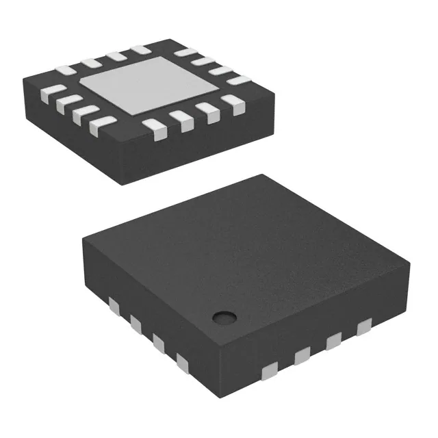


 工商网监
湘ICP备2023018690号
工商网监
湘ICP备2023018690号
