Si5348 Rev E Data Sheet
Network Synchronizer for SyncE/ 1588 PTP Telecom Boundary
(T-BC) and Slave (T-SC) Clocks
KEY FEATURES
The Si5348 combines the industry’s smallest footprint and lowest power network synchronizer clock with unmatched frequency synthesis flexibility and ultra-low jitter. The
Si5348 is ideally suited for wireless backhaul, IP radio, small and macro cell wireless
communications systems, and data center switches requiring both traditional and packet
based network synchronization.
• Three independent DSPLLs in a single
monolithic IC supporting flexible SyncE/
IEEE 1588 and SETS architectures
The three independent DSPLLs™ are individually configurable as a SyncE PLL, IEEE
1588 DCO or a general-purpose PLL for processor/FPGA clocking. The Si5348 can also
be used in legacy SETS systems needing Stratum 3/3E compliance. The optional digitally controlled oscillator (DCO) mode provides precise timing adjustment to 1 ppt for 1588
(PTP) clock steering applications. The unique design of the Si5348 allows the TCXO/
OCXO reference input to determine the device’s frequency accuracy and stability. The
Si5348 is programmable via a serial interface with in-circuit programmable non-volatile
memory so it always powers up into a known configuration. Programming the Si5348 is
easy with ClockBuilder Pro™ software. Factory pre-programmed devices are also available.
• Input frequency range:
• External crystal: 48 to 54 MHz
Applications:
• Synchronous Ethernet (SyncE) ITU-T G.8262 EEC Option 1 & 2
• Telecom Boundary Clock (T-BC) as defined by ITU-T G.8273.2
• IEEE 1588 (PTP) slave clock synchronization
• Stratum 3/3E, G.812, G.813 network synchronization
• Ultra-low jitter of 95 fs
• Enhanced hitless switching minimizes
output phase transients
• REF clock: 5 to 250 MHz
• Diff clock: 8 kHz to 750 MHz
• LVCMOS clock: 8 kHz to 250 MHz
• Output frequency range:
• Differential: 1 PPS to 718.5 MHz
• LVCMOS: 1 PPS to 250 MHz
• Meets the requirements of:
• ITU-T G.8262 (SyncE) EEC Options 1
and 2
• ITU-T G.812 Type III, IV
• ITU-T G.813 Option 1
• Telcordia GR-1244, GR-253
(Stratum-3/3E)
48-54 MHz XTAL
XA
TCXO/
OCXO
XB
OSC
REF
REFb
IN3
IN4
DSPLL D
IN0
÷FRAC
IN1
÷FRAC
IN2
DSPLL C
÷FRAC
DSPLL A
Status Flags
I2C / SPI
÷INT
OUT0
÷INT
OUT1
÷INT
OUT2
÷INT
OUT3
÷INT
OUT4
÷INT
OUT5
÷INT
OUT6
Status Monitor
Control
NVM
Si5348
silabs.com | Building a more connected world.
This information applies to a product under development. Its characteristics and specifications are subject to change without notice.
Preliminary Rev. 0.95
�Si5348 Rev E Data Sheet
Feature List
1. Feature List
The Si5348 features are listed below:
• Three independent DSPLLs in a single monolithic IC supporting flexible SyncE/IEEE 1588 and SETS architectures
• Ultra-Low Jitter
• 95 fs typ (12 kHz to 20 MHz)
• Meets the requirements of:
• ITU-T G.8273.2 T-BC
• ITU-T G.8262 (SyncE) EEC Options 1 & 2
• ITU-T G.812 Type III, IV
• ITU-T G.813 Option 1
• Telcordia GR-1244, GR-253 (Stratum-3/3E)
• Each DSPLL generates any output frequency from any input
frequency
• Input frequency range:
• External crystal: 48–54 MHz
• REF clock: 5–250 MHz
• Diff clock: 8 kHz–750 MHz
• LVCMOS clock: 8 kHz–250 MHz
• Output frequency range:
• Differential: 1 PPS to 718.5 MHz
• LVCMOS: 1 PPS to 250 MHz
• Independent Frequency-on-the-fly for each DSPLL
• Enhanced hitless switching minimizes output phase transients for 8 kHz, 19.44 MHz, 25 MHz, and other input frequencies.
silabs.com | Building a more connected world.
• Pin or software controllable DCO on each DSPLL with typical
resolution to 1 ppt/step
• TCXO/OCXO reference input determines DSPLL free-run/holdover accuracy and stability
• Programmable jitter attenuation bandwidth per DSPLL: 0.001
Hz to 4 kHz
• Highly configurable output drivers: LVDS, LVPECL, LVCMOS,
HCSL, CML
• Core voltage:
• VDD: 1.8 V ±5%
• VDDA: 3.3 V ±5%
• Independent output supply pins: 3.3 V, 2.5 V, or 1.8 V
• Built-in power supply filtering
• Status monitoring: LOS, OOF, LOL
• Serial Interface: I2C or SPI (3-wire or 4-wire)
• ClockBuilderTM Pro software tool simplifies device configuration
• 5 input, 7 output, 64 QFN
• Temperature range: –40 to +85 °C
• Pb-free, RoHS-6 compliant
Preliminary Rev. 0.95 | 2
�Si5348 Rev E Data Sheet
Related Documents
2. Related Documents
Table 2.1. Related Documentation and Software
Document/Resource
Si5348 Rev E Family Reference Manual
Crystal Reference Manual
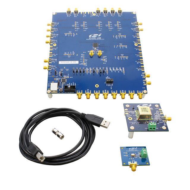
Si5348 EVB User Guide
Frequently Asked Questions
Quality and Reliability
Description/URL
To be used in conjunction with this data sheet, which contains more detailed explanations about the operation of the device.
https://www.silabs.com/documents/public/reference-manuals/si534x-8x-recommended-crystals-rm.pdf
Instructions about how to use the evaluation kits.
TBD
http://www.silabs.com/quality
Development Kits
https://www.silabs.com/products/development-tools/timing/clock#highperformance
ClockBuilder Pro (CBPro) Software
https://www.silabs.com/products/development-tools/software/clockbuilderpro-software
AN1077: Selecting the Right Clocks for Timing Synchro- https://www.silabs.com/documents/public/application-notes/an1077-selectnization Applications
ing-clocks-for-timing-synchronization.pdf
UG123: SiOCXO1-EVB Evaluation Board Users Guide
https://www.silabs.com/documents/public/user-guides/UG123.pdf
UGTBD: SiTCXO1-EVB Evaluation Board User's Guide Link TBD
ANTBDX: Holdover Consideration for Si5348 Network
Synchronizer
silabs.com | Building a more connected world.
Link TBD
Preliminary Rev. 0.95 | 3
�Si5348 Rev E Data Sheet
Ordering Guide
3. Ordering Guide
Table 3.1. Si5348 Ordering Guide
Ordering Part Number
Si5348A-E-GM 1, 2
Si5348B-E-GM 1, 2
# of
DSPLLs
3
Output Clock Frequency
Range
1 Hz to 718.5 MHz
1 Hz to 350 MHz
Package
RoHS-6, Pb-Free
Temperature
Range
64-Lead 9x9 QFN
Yes
–40 to 85 °C
Si5348-E-EVB
—
—
Evaluation Board
—
—
SiOCXO1-EVB
—
12.800 MHz
OCXO Evaluation
Board
—
—
Note:
1. Add an R at the end of the device part number to denote tape and reel ordering options.
2. Custom, factory pre-programmed devices are available. Ordering part numbers are assigned by the ClockBuilder Pro software.
Part number format is: Si5348A-Dxxxxx-GM, where “xxxxx” is a unique numerical sequence representing the pre-programmed
configuration.
Si534fg-Rxxxxx-GM
Timing product family
f = Packet Network Synchronizer for SyncE/1588 (8)
g = Device grade (A, B)
Product Revision*
Custom ordering part number (OPN) sequence ID**
Package, ambient temperature range (QFN, -40 °C to +85°C)
*See Ordering Guide table for current product revision
** 5 digits; assigned by ClockBuilder Pro
Figure 3.1. Ordering Part Number Fields
silabs.com | Building a more connected world.
Preliminary Rev. 0.95 | 4
�Table of Contents
1. Feature List . . . . . . . . . . . . . . . . . . . . . . . . . . . . . . . . 2
2. Related Documents . . . . . . . . . . . . . . . . . . . . . . . . . . . . . 3
3. Ordering Guide
. . . . . . . . . . . . . . . . . . . . . . . . . . . . . . 4
4. Functional Description. . . . . . . . . . . . . . . . . . . . . . . . . . . . 7
4.1 Standards Compliance .
.
.
.
.
.
.
.
.
.
.
.
.
.
.
.
.
.
.
.
.
.
.
.
.
.
. 7
4.2 Frequency Configuration
.
.
.
.
.
.
.
.
.
.
.
.
.
.
.
.
.
.
.
.
.
.
.
.
.
. 7
4.3 DSPLL Loop Bandwidth .
4.3.1 Fastlock Feature . .
.
.
.
.
.
.
.
.
.
.
.
.
.
.
.
.
.
.
.
.
.
.
.
.
.
.
.
.
.
.
.
.
.
.
.
.
.
.
.
.
.
.
.
.
.
.
.
.
.
.
. 7
. 8
4.4 Modes of Operation . .
4.4.1 Initialization and Reset
4.4.2 Free-run Mode . .
4.4.3 Lock Acquisition Mode
4.4.4 Locked Mode . . .
4.4.5 Holdover Mode . .
4.4.6 Frequency on the Fly
.
.
.
.
.
.
.
.
.
.
.
.
.
.
.
.
.
.
.
.
.
.
.
.
.
.
.
.
.
.
.
.
.
.
.
.
.
.
.
.
.
.
.
.
.
.
.
.
.
.
.
.
.
.
.
.
.
.
.
.
.
.
.
.
.
.
.
.
.
.
.
.
.
.
.
.
.
.
.
.
.
.
.
.
.
.
.
.
.
.
.
.
.
.
.
.
.
.
.
.
.
.
.
.
.
.
.
.
.
.
.
.
.
.
.
.
.
.
.
.
.
.
.
.
.
.
.
.
.
.
.
.
.
.
.
.
.
.
.
.
.
.
.
.
.
.
.
.
.
.
.
.
.
.
.
.
.
.
.
.
.
.
.
.
.
.
.
.
.
.
.
.
.
.
.
. 8
. 8
. 8
. 9
. 9
. 9
.10
4.5 Digitally-Controlled Oscillator (DCO) Mode
.
.
.
.
.
.
.
.
.
.
.
.
.
.
.
.
.
.
.
.10
4.6 External Reference (XA/XB, REF/REFb) .
4.6.1 External Crystal (XA/XB) . . . . .
4.6.2 External Reference (REF/REFb) . .
.
.
.
.
.
.
.
.
.
.
.
.
.
.
.
.
.
.
.
.
.
.
.
.
.
.
.
.
.
.
.
.
.
.
.
.
.
.
.
.
.
.
.
.
.
.
.
.
.
.
.
.
.
.
.
.
.
.10
.11
.12
4.7 Inputs (IN0, IN1, IN2, REF, IN3, IN4) . .
4.7.1 Input Selection . . . . . . . .
4.7.2 Manual Input Selection . . . . . .
4.7.3 Automatic Input Selection . . . . .
4.7.4 Input Configuration and Terminations .
4.7.5 Hitless Input Switching . . . . . .
4.7.6 Ramped Input Switching . . . . .
4.7.7 Glitchless Input Switching . . . . .
4.7.8 Typical Hitless Switching Scenarios .
4.7.9 Synchronizing to Gapped Input Clocks
.
.
.
.
.
.
.
.
.
.
.
.
.
.
.
.
.
.
.
.
.
.
.
.
.
.
.
.
.
.
.
.
.
.
.
.
.
.
.
.
.
.
.
.
.
.
.
.
.
.
.
.
.
.
.
.
.
.
.
.
.
.
.
.
.
.
.
.
.
.
.
.
.
.
.
.
.
.
.
.
.
.
.
.
.
.
.
.
.
.
.
.
.
.
.
.
.
.
.
.
.
.
.
.
.
.
.
.
.
.
.
.
.
.
.
.
.
.
.
.
.
.
.
.
.
.
.
.
.
.
.
.
.
.
.
.
.
.
.
.
.
.
.
.
.
.
.
.
.
.
.
.
.
.
.
.
.
.
.
.
.
.
.
.
.
.
.
.
.
.
.
.
.
.
.
.
.
.
.
.
.
.
.
.
.
.
.
.
.
.
.13
.13
.13
.13
.14
.14
.14
.14
.15
.16
4.8 Fault Monitoring . . . .
4.8.1 Input LOS Detection. .
4.8.2 XA/XB LOS Detection .
4.8.3 OOF Detection . . .
4.8.4 Precision OOF Monitor .
4.8.5 Fast OOF Monitor . .
4.8.6 LOL Detection . . . .
4.8.7 Interrupt Pin (INTRb) .
.
.
.
.
.
.
.
.
.
.
.
.
.
.
.
.
.
.
.
.
.
.
.
.
.
.
.
.
.
.
.
.
.
.
.
.
.
.
.
.
.
.
.
.
.
.
.
.
.
.
.
.
.
.
.
.
.
.
.
.
.
.
.
.
.
.
.
.
.
.
.
.
.
.
.
.
.
.
.
.
.
.
.
.
.
.
.
.
.
.
.
.
.
.
.
.
.
.
.
.
.
.
.
.
.
.
.
.
.
.
.
.
.
.
.
.
.
.
.
.
.
.
.
.
.
.
.
.
.
.
.
.
.
.
.
.
.
.
.
.
.
.
.
.
.
.
.
.
.
.
.
.
.17
.17
.18
.18
.18
.18
.19
.20
.
.
.
.
.
.
.
.
.
.
.
.
.
.
.
.
.
.
.
.
.
.
.
.
.
.
.
.
.
.
.
.
.
.
.
.
.
.
.
.
.
.
.
.
.
.
.
.
.
.
.
.
.
.
.
.20
.20
.20
.20
.20
.
.
.
.
.
.
.
.
.
.
.
.
.
.
.
.
.
.
.
.
.
.
.
.
.
.
.
.
.
.
.
.
.
.
.
.
.
.
.
.
4.9 Outputs . . . . . . . . . . . . . . . . . . . .
4.9.1 Output Crosspoint . . . . . . . . . . . . . . .
4.9.2 Support For 1 Hz Output . . . . . . . . . . . . .
4.9.3 Output Signal Format . . . . . . . . . . . . . .
4.9.4 Programmable Common Mode Voltage For Differential Outputs
silabs.com | Building a more connected world.
Preliminary Rev. 0.95 | 5
�4.9.5 LVCMOS Output Impedance Selection . .
4.9.6 LVCMOS Output Signal Swing . . . . .
4.9.7 LVCMOS Output Polarity . . . . . . .
4.9.8 Output Enable/Disable . . . . . . . .
4.9.9 Output Disable During LOL . . . . . .
4.9.10 Output Disable During XAXB_LOS . . .
4.9.11 Output Driver State When Disabled . . .
4.9.12 Synchronous/Asynchronous Output Disable
4.9.13 Output Divider (R) Synchronization . . .
4.10 Power Management .
.
.
.
.
.
.
.
.
.
.
.
.
.
.
.
.
.
.
.
.
.
.
.
.
.
.
.
.
.
.
.
.
.
.
.
.
.
.
.
.
.
.
.
.
.
.
.
.
.
.
.
.
.
.
.
.
.
.
.
.
.
.
.
.
.
.
.
.
.
.
.
.
.
.
.
.
.
.
.
.
.
.
.
.
.
.
.
.
.
.
.
.
.
.
.
.
.
.
.
.
.
.
.
.
.
.
.
.
.
.
.
.
.
.
.
.
.
.
.
.
.
.
.
.
.
.
.
.
.
.
.
.
.
.
.
.
.
.
.
.
.
.
.
.
.
.
.
.
.
.
.
.
.
.21
.21
.21
.21
.21
.21
.21
.21
.22
.
.
.
.
.
.
.
.
.
.
.
.
.
.
.
.
.
.
.
.
.
.
.
.
.
.
.22
4.11 In-Circuit Programming .
.
.
.
.
.
.
.
.
.
.
.
.
.
.
.
.
.
.
.
.
.
.
.
.
.
.22
4.12 Serial Interface
.
.
.
.
.
.
.
.
.
.
.
.
.
.
.
.
.
.
.
.
.
.
.
.
.
.22
4.13 Custom Factory Preprogrammed Parts .
.
.
.
.
.
.
.
.
.
.
.
.
.
.
.
.
.
.
.
.22
5. Register Map
.
.
.
. . . . . . . . . . . . . . . . . . . . . . . . . . . . . . 23
6. Electrical Specifications
. . . . . . . . . . . . . . . . . . . . . . . . . . 24
7. Typical Application Schematic . . . . . . . . . . . . . . . . . . . . . . . .
8. Detailed Block Diagram
39
. . . . . . . . . . . . . . . . . . . . . . . . . . 40
9. Typical Operating Characteristics (Jitter and Phase Noise)
. . . . . . . . . . . . . 41
10. Pin Descriptions. . . . . . . . . . . . . . . . . . . . . . . . . . . . .
42
11. Package Outline . . . . . . . . . . . . . . . . . . . . . . . . . . . . .
46
12. PCB Land Pattern
13. Top Marking
. . . . . . . . . . . . . . . . . . . . . . . . . . . . 47
. . . . . . . . . . . . . . . . . . . . . . . . . . . . . . 49
14. Device Errata . . . . . . . . . . . . . . . . . . . . . . . . . . . . . . 50
15. Revision History. . . . . . . . . . . . . . . . . . . . . . . . . . . . .
silabs.com | Building a more connected world.
51
Preliminary Rev. 0.95 | 6
�Si5348 Rev E Data Sheet
Functional Description
4. Functional Description
The Si5348 offers three DSPLLs that have identical performance and flexibility which can be independently configured and controlled
through the serial interface. Each of the DSPLLs support locked, free-run, and holdover modes of operation with an optional DCO mode
for IEEE 1588 applications. The device requires an external crystal and an external reference (TCXO or OCXO) to operate. The reference input (REF/REFb) determines the frequency accuracy and stability while in free-run and holdover modes. The external crystal
completes the internal oscillator circuit (OSC) which is used by the DSPLL for intrinsic jitter performance. There are three main inputs
(IN0 - IN2) for synchronizing the DSPLLs. Input selection can be manual or automatically controlled using an internal state machine.
Two additional manually selected inputs are available to DSPLL D. Any of the output clocks (OUT0 to OUT6) can be configured to any
of the DSPLLs using a flexible crosspoint connection. Output 6 is the only output that can be configured for a 1 Hz output to support 1
PPS.
4.1 Standards Compliance
Each of the DSPLLs meet the requirements of ITU-T G.8262 (SyncE), G.812, G.813, G.8273.2 (T-BC), in addition to Telcordia
GR-1244 and GR-253 as shown in the compliance report. The DCO feature enables IEEE1588 (PTP) implementations in addition to
hybrid SyncE + IEEE1588 (T-BC). The following table lists the Si5348 compliance reports for these standards.
Table 4.1. Si5348 Standards Compliance Reports
Standard
Compliance Report
G.8262 (SyncE)
https://www.silabs.com/documents/public/miscellaneous/Si5348_SynchronousEthernet-G.8262_ComplianceTestResults_Rev1.0.pdf
G.812
https://www.silabs.com/documents/public/miscellaneous/Si5348_ITU-T_G.812_ComplianceTestResults_Rev1.0.pdf
G.813
https://www.silabs.com/documents/public/miscellaneous/Si5348_ITU-T_G.813_ComplianceTestResults_Rev1.0.pdf
GR-1244
https://www.silabs.com/documents/public/miscellaneous/Si5348_Telcordia_GR-1244_ComplianceTestResults_Rev1.0.pdf
GR-253
https://www.silabs.com/documents/public/miscellaneous/Si5348_Telcordia_GR-253_ComplianceTestResults_Rev1.0.pdf
4.2 Frequency Configuration
The frequency configuration for each of the DSPLLs is programmable through the serial interface and can also be stored in non-volatile
memory. The combination of fractional input dividers (Pn/Pd), fractional frequency multiplication (Mn/Md), and integer output division
(Rn) allows each of the DSPLLs to lock to any input frequency and generate virtually any output frequency. All divider values for a
specific frequency plan are easily determined using the ClockBuilder Pro utility. Each PLL can be reconfigured during operation without
affecting the others. See 4.4.6 Frequency on the Fly for more information.
4.3 DSPLL Loop Bandwidth
The DSPLL loop bandwidth determines the amount of input clock jitter and wander attenuation. Register configurable DSPLL loop
bandwidth settings of 1 mHz to 4 kHz are available for selection for each of the DSPLLs. Since the loop bandwidth is controlled digitally,
each of the DSPLLs will always remain stable with less than 0.1 dB of peaking regardless of the loop bandwidth selection.
Table 4.2. Loop Bandwidth Requirements for North America
SONET (Telcordia)
SDH (ITU-T)
SyncE (ITU-T)
Loop Bandwidth
GR-253 Stratum 3E
G.812 Type III
—
0.001 Hz
GR-253 Stratum 3
G.812 Type IV
G.8262 EEC Option 2
10 ppm
Fpfd < 500 kHz
Fpfd ≥ 500 kHz
Ramped Exit from Holdover
Ramped Input Switching and Ramped Exit from Holdover
Ramped Exit from Holdover
Ramped Input Switching and Ramped Exit from Holdover
4.7.7 Glitchless Input Switching
The DSPLLs have the ability of switching between two input clock frequencies that are up to ±500 ppm apart. The DSPLL will pull-in to
the new frequency using the DSPLL Loop Bandwidth or using the Fastlock Loop Bandwidth if it is enabled. The loss of lock (LOL) indicator will assert while the DSPLL is pulling-in to the new clock frequency. There will be no output runt pulses generated at the output
during the transition. All clock inputs, including 3 and 4, support glitchless input switching.
silabs.com | Building a more connected world.
Preliminary Rev. 0.95 | 14
�Si5348 Rev E Data Sheet
Functional Description
4.7.8 Typical Hitless Switching Scenarios
Figure 4.7. Output Frequency Transient—Ramped Switching between Two 8 kHz Inputs (±4.6 ppm Offset)
Figure 4.8. Output Phase Transient—Hitless Switching between Two 25 MHz Inputs (0 ppm, 180 Degree Phase Shift)
silabs.com | Building a more connected world.
Preliminary Rev. 0.95 | 15
�Si5348 Rev E Data Sheet
Functional Description
4.7.9 Synchronizing to Gapped Input Clocks
Each of the DSPLLs support locking to an input clock that has missing periods. This is also referred to as a gapped clock. The purpose
of gapped clocking is to modulate the frequency of a periodic clock by selectively removing some of its cycles. Gapping a clock severely
increases its jitter, so a phase-locked loop with high jitter tolerance and low loop bandwidth is required to produce a low-jitter periodic
clock. The resulting output will be a periodic non-gapped clock with an average frequency of the input with its missing cycles. For example, an input clock of 100 MHz with one cycle removed every 10 cycles will result in a 90 MHz periodic non-gapped output clock. This is
shown in the figure below:
Gapped Input Clock
Periodic Output Clock
100 MHz clock
1 missing period every 10
90 MHz non-gapped clock
100 ns
100 ns
DSPLL
1
10 ns
2
3
4
5
6
7
8
9
Period Removed
10
1
2
3
4
5
6
7
8
9
11.11111... ns
Figure 4.9. Generating an Averaged Clock Output Frequency from a Gapped Clock Input
A valid gapped clock input must have a minimum frequency of 10 MHz with a maximum of two missing cycles out of every eight. Locking to a gapped clock will not trigger the LOS, OOF, and LOL fault monitors. Clock switching between gapped clocks may violate the
hitless switching specification in Table 6.8 Performance Characteristics on page 32 when the switch occurs during a gap in either
input clock.
silabs.com | Building a more connected world.
Preliminary Rev. 0.95 | 16
�Si5348 Rev E Data Sheet
Functional Description
4.8 Fault Monitoring
Three input clocks (IN0, IN1, IN2) and the reference input (REF/REFb) are monitored for loss of signal (LOS) and out-of-frequency
(OOF) as shown in the figure below. The reference at the XA/XB pins is also monitored for LOS since it provides a critical reference
clock for the DSPLLs. Each of the DSPLLs also has an LOL indicator, which is asserted when synchronization is lost with their selected
input clock. IN3 and IN4 can be monitored, but, at most, four input clocks can be monitored simultaneously.
XA
XB
OSC
Si5348
LOS
DSPLL B
REF
LOS
÷ PREF
REFb
Input
Crosspoint
IN0
÷
IN0b
P0n
P0d
OOF
LOS
Precision
Fast
LOL
0
1
2
PD
3
P1n
÷
P1d
IN1
IN1b
Precision
OOF
Fast
LOS
÷
IN2b
P2n
P2d
OOF
LOS
Precision
Fast
LOL
0
1
2
PD
LOS
IN4
LOS
DSPLL C
LPF
÷M
0
1
2
LOL
PD
3
4
5
IN3
LPF
÷M
3
IN2
DSPLL A
DSPLL D
LPF
÷M
Figure 4.10. Si5348 Fault Monitors
4.8.1 Input LOS Detection
The loss of signal monitor measures the period of each input clock cycle to detect phase irregularities or missing clock edges. Each of
the input LOS circuits has its own programmable sensitivity which allows ignoring missing edges or intermittent errors. Loss of signal
sensitivity is configurable using the ClockBuilder Pro utility. The LOS status for each of the monitors is accessible by reading a status
register. The live LOS register always displays the current LOS state and a sticky register, when set, always stays asserted until
cleared. When DSPLLD is configured to use both IN3 and IN4 the LOS outputs are not connected to the holdover entry/exit logic. When
configured for one of either IN3 or IN4 (but not both) the LOS for the input clock is connected to the holdover entry/exit logic.
Monitor
Sticky
LOS
LOS
LOS
en
Live
Figure 4.11. LOS Status Indicators
silabs.com | Building a more connected world.
Preliminary Rev. 0.95 | 17
�Si5348 Rev E Data Sheet
Functional Description
4.8.2 XA/XB LOS Detection
A LOS monitor is available to ensure that the external crystal or reference clock is valid. By default the output clocks are disabled when
XAXB_LOS is detected. This feature can be disabled such that the device will continue to produce output clocks when XAXB_LOS is
detected.
4.8.3 OOF Detection
Input clocks IN0, IN1, IN2 are monitored for frequency accuracy with respect to an OOF reference, which it considers as its “0_ppm”
reference. Since a TCXO or OCXO will be connected to the REF input, most applications will declare the REF input to be the OOF
reference. The final OOF status is determined by the combination of both a precise OOF monitor and a fast OOF monitor as shown in
the figure below. An option to disable either monitor is also available. The live OOF register always displays the current OOF state and
its sticky register bit stays asserted until cleared.
Monitor
OOF
Sticky
en
Precision
LOS
OOF
Fast
Live
en
Figure 4.12. OOF Status Indicator
4.8.4 Precision OOF Monitor
The precision OOF monitor circuit measures the frequency of all input clocks to within ±1/16 ppm accuracy with respect to the selected
OOF frequency reference. A valid input clock frequency is one that remains within the OOF frequency range, which is register configurable up to ±500 ppm in steps of 1/16 ppm. A configurable amount of hysteresis is also available to prevent the OOF status from toggling at the failure boundary. An example is shown in the figure below. In this case, the OOF monitor is configured with a valid frequency range of ±6 ppm and with 2 ppm of hysteresis. An option to use one of the input pins (IN0 – IN2) as the 0 ppm OOF reference
instead of the REF/REFb pins is available. This option is register-configurable. XA/XB can also be used as the 0 ppm reference.
OOF Declared
fIN
Hysteresis
Hysteresis
OOF Cleared
-6 ppm
(Set)
-4 ppm
(Clear)
0 ppm
OOF Reference
+4 ppm
(Clear)
+6 ppm
(Set)
Figure 4.13. Example of Precise OOF Monitor Assertion and De-assertion Triggers
4.8.5 Fast OOF Monitor
Because the precision OOF monitor needs to provide 1/16 ppm of frequency measurement accuracy, it must measure the monitored
input clock frequencies over a relatively long period of time. This may be too slow to detect an input clock that is quickly ramping in
frequency. An additional level of OOF monitoring called the Fast OOF monitor runs in parallel with the precision OOF monitors to quickly detect a ramping input frequency. The Fast OOF monitor asserts OOF on an input clock frequency that has changed by greater than
±4000 ppm.
silabs.com | Building a more connected world.
Preliminary Rev. 0.95 | 18
�Si5348 Rev E Data Sheet
Functional Description
4.8.6 LOL Detection
There is an LOL monitor for each of the DSPLLs. The LOL monitor asserts the LOL register bit when a DSPLL has lost synchronization
with its selected input clock. There is also a dedicated loss of lock pin that reflects the loss of lock condition for each of the DSPLLs
(LOL_Ab, LOL_Cb, LOL_Db) and also for the reference. There are two LOL frequency monitors, one that sets the LOL indicator (LOL
Set) and another that clears the indicator (LOL Clear). An optional timer is available to delay clearing of the LOL indicator to allow additional time for the DSPLL to completely lock to the input clock. The timer is also useful to prevent the LOL indicator from toggling or
chattering as the DSPLL completes lock acquisition. A block diagram of the LOL monitor is shown in the figure below. The live LOL
register always displays the current LOL state and a sticky register always stays asserted until cleared. The LOLb pin reflects the current state of the LOL monitor.
Si5348
Sticky
LOS
LOL Status Registers
Live
DSPLL D
DSPLL C
DSPLL A
LOL Monitor
LOL_Db
LOL
Clear
t
LOL_Cb
LOL_Ab
LOL
Set
DSPLL A
fIN
PD
LPF
÷M
Figure 4.14. LOL Status Indicators
Each of the LOL frequency monitors has adjustable sensitivity, which is register-configurable from 0.1 ppm to 10,000 ppm. Having two
separate frequency monitors allows for hysteresis to help prevent chattering of LOL status. An example configuration where LOCK is
indicated when there is less than 0.1 ppm frequency difference at the inputs of the phase detector and LOL is indicated when there is
more than 1 ppm frequency difference is shown in Figure 4.15 LOL Set and Clear Thresholds on page 19.
Clear LOL
Threshold
Set LOL
Threshold
Lock Acquisition
LOL
Hysteresis
Lost Lock
LOCKED
0
0.1
1
10,000
Phase Detector Frequency Difference (ppm)
Figure 4.15. LOL Set and Clear Thresholds
An optional timer is available to delay clearing of the LOL indicator to allow additional time for the DSPLL to completely lock to the input
clock. The timer is also useful to prevent the LOL indicator from toggling or chattering as the DSPLL completes lock acquisition. The
silabs.com | Building a more connected world.
Preliminary Rev. 0.95 | 19
�Si5348 Rev E Data Sheet
Functional Description
configurable delay value depends on frequency configuration and loop bandwidth of the DSPLL and is automatically calculated using
the ClockBuilderPro utility.
4.8.7 Interrupt Pin (INTRb)
An interrupt pin (INTRb) indicates a change in state with any of the status indicators for any of the DSPLLs. All status indicators are
maskable to prevent assertion of the interrupt pin. The state of the INTRb pin is reset by clearing the sticky status registers.
4.9 Outputs
The Si5348 supports seven differential output drivers. Each driver has a configurable voltage amplitude and common mode voltage
covering a wide variety of differential signal formats including LVPECL, LVDS, HCSL, and CML. In addition to supporting differential
signals, any of the outputs can be configured as single-ended LVCMOS (3.3 V, 2.5 V, or 1.8 V) providing up to 14 single-ended outputs,
or a combination of differential and single-ended outputs.
4.9.1 Output Crosspoint
A crosspoint allows any of the output drivers to connect with any of the DSPLLs as shown in the figure below. The crosspoint configuration is programmable and can be stored in NVM so that the desired output configuration is ready at power-up.
4.9.2 Support For 1 Hz Output
Output 6 of the Si5348 can be configured to generate a 1 Hz clock by cascading the R5 and R6 dividers. Output 5 is still usable in this
case but is limited to a maximum frequency of 33.5 MHz. ClockBuilder Pro automatically determines the optimum configuration when
generating a 1 Hz output (1 PPS).
A
C
D
÷R4
VDDO4
OUT4
OUT4b
A
C
D
÷R5
VDDO5
OUT5
OUT5b
÷R6
VDDO6
OUT6
OUT6b
R5
A
C
D
Figure 4.16. Generating a 1 Hz Output using the Si5348
4.9.3 Output Signal Format
The differential output amplitude and common mode voltage are both programmable and compatible with a wide variety of signal formats, including LVDS and LVPECL. In addition to supporting differential signals, any of the outputs can be configured as LVCMOS (3.3
V, 2.5 V, or 1.8 V) drivers providing up to 14 single-ended outputs or a combination of differential and single-ended outputs.
4.9.4 Programmable Common Mode Voltage For Differential Outputs
The common mode voltage (VCM) for the differential modes is programmable and depends on the voltage available at the output’s
VDDO pin. Setting the common mode voltage is useful when dc-coupling the output drivers.
silabs.com | Building a more connected world.
Preliminary Rev. 0.95 | 20
�Si5348 Rev E Data Sheet
Functional Description
4.9.5 LVCMOS Output Impedance Selection
Each LVCMOS driver has a configurable output impedance to accommodate different trace impedances and drive strengths. A source
termination resistor is recommended to help match the selected output impedance to the trace impedance. There are three programmable output impedance selections for each VDDO options as shown in the table below. Note that selecting a lower source impedance
may result in higher output power consumption.
Table 4.5. Typical Output Impedance (ZS)
VDDO
CMOS_DRIVE_Selection
OUTx_CMOS_DRV=1
OUTx_CMOS_DRV=2
OUTx_CMOS_DRV=3
3.3 V
38 Ω
30 Ω
22 Ω
2.5 V
43 Ω
35 Ω
24 Ω
1.8 V
—
46 Ω
31 Ω
4.9.6 LVCMOS Output Signal Swing
The signal swing (VOL/VOH) of the LVCMOS output drivers is set by the voltage on the VDDO pins. Each output driver has its own
VDDO pin allowing a unique output voltage swing for each of the LVCMOS drivers.
4.9.7 LVCMOS Output Polarity
When a driver is configured as an LVCMOS output, it generates a clock signal on both pins (OUTx and OUTxb). By default the clock on
the OUTxb pin is generated with the same polarity (in phase) with the clock on the OUTx pin. The polarity of these clocks is configurable, which enables complementary clock generation and/or inverted polarity with respect to other output drivers.
4.9.8 Output Enable/Disable
The Si5348 allows enabling/disabling outputs by pin or register control, or a combination of both. Three output enable pins are available
(OE0b, OE1b, OE2b). The output enable pins can be mapped to any of the outputs (OUTx) through register configuration. By default
OE0b controls all of the outputs while OE1b and OE2b remain unmapped and has no effect until configured. The figure below shows an
example of an output enable mapping scheme that is register configurable and can be stored in NVM as the default at power-up.
Enabling and disabling outputs can also be controlled by register control. This allows disabling one or more output when the OEb pin(s)
has them enabled. By default the output enable register settings are configured to allow the OEb pins to have full control.
4.9.9 Output Disable During LOL
By default a DSPLL that is out of lock will generate either free-running clocks or generate clocks in holdover mode. There is an option to
disable the outputs when a DSPLL is LOL. This option can be useful to force a downstream PLL into holdover.
4.9.10 Output Disable During XAXB_LOS
The internal oscillator circuit (OSC) in combination with the external crystal (XTAL) provides a critical function for the operation of the
DSPLLs. In the event of a crystal failure the device will assert an XAXB_LOS alarm. By default all outputs will be disabled during assertion of the XAXB_LOS alarm. There is an option to leave the outputs enabled during an XAXB_LOS alarm, but the frequency accuracy
and stability will be indeterminate during this fault condition.
4.9.11 Output Driver State When Disabled
The disabled state of an output driver is register configurable as disable low or high.
4.9.12 Synchronous/Asynchronous Output Disable
Outputs can be configured to disable synchronously or asynchronously. In synchronous disable mode the output will wait until a clock
period has completed before the driver is disabled. This prevents unwanted runt pulses from occurring when disabling an output. In
asynchronous disable mode, the output clock will disable immediately without waiting for the period to complete.
silabs.com | Building a more connected world.
Preliminary Rev. 0.95 | 21
�Si5348 Rev E Data Sheet
Functional Description
4.9.13 Output Divider (R) Synchronization
All the output R dividers are reset to a known state during the power-up initialization period. This ensures consistent and repeatable
phase alignment across all output drivers. Resetting the device using the RSTb pin or asserting the hard reset bit will have the same
result.
4.10 Power Management
Unused inputs, output drivers, and DSPLLs can be powered down when unused.
4.11 In-Circuit Programming
The Si5348 is fully configurable using the serial interface (I2C or SPI). At power-up the device downloads its default register values from
internal non-volatile memory (NVM). Application specific default configurations can be written into NVM allowing the device to generate
specific clock frequencies at power-up. Writing default values to NVM is in-circuit programmable with normal operating power supply
voltages applied to its VDD and VDDA pins. The NVM is two time writable. Once a new configuration has been written to NVM, the old
configuration is no longer accessible.
4.12 Serial Interface
Configuration and operation of the Si5348 is controlled by reading and writing registers using the I2C or SPI interface. The I2C_SEL pin
selects I2C or SPI operation. Communication with both 3.3 V and 1.8 V host is supported. The SPI mode operates in either 4-wire or 3wire mode.
4.13 Custom Factory Preprogrammed Parts
For applications where a serial interface is not available for programming the device, custom pre-programmed parts can be ordered
with a specific configuration written into NVM. A factory pre-programmed part will generate clocks at power-up. Custom, factory-preprogrammed devices are available. Use the ClockBuilder Pro custom part number wizard (www.silabs.com/clockbuilderpro) to quickly
and easily request and generate a custom part number for your configuration.
In less than three minutes, you will be able to generate a custom part number with a detailed data sheet addendum matching your
design’s configuration. Once you receive the confirmation email with the data sheet addendum, simply place an order with your local
Silicon Labs sales representative. Samples of your pre-programmed device will typically ship in about two weeks.
silabs.com | Building a more connected world.
Preliminary Rev. 0.95 | 22
�Si5348 Rev E Data Sheet
Register Map
5. Register Map
Refer to the Si5348 Rev E Reference Manual for a complete list of register descriptions and settings.
silabs.com | Building a more connected world.
Preliminary Rev. 0.95 | 23
�Si5348 Rev E Data Sheet
Electrical Specifications
6. Electrical Specifications
Table 6.1. Recommended Operating Conditions
Parameter
Symbol
Min
Typ
Max
Unit
Ambient Temperature
TA
–40
25
85
°C
Junction Temperature
TJMAX
—
—
125
°C
VDD
1.71
1.80
1.89
V
VDDA
3.14
3.30
3.47
V
3.14
3.30
3.47
V
2.37
2.50
2.62
V
1.71
1.80
1.89
V
3.14
3.30
3.47
V
1.71
1.80
1.89
V
Core Supply Voltage
Output Driver Supply Voltage
Status Pin Supply Voltage
VDDO
VDDS
Note:
1. All minimum and maximum specifications are guaranteed and apply across the recommended operating conditions. Typical values apply at nominal supply voltages and an operating temperature of 25 °C unless otherwise noted.
silabs.com | Building a more connected world.
Preliminary Rev. 0.95 | 24
�Si5348 Rev E Data Sheet
Electrical Specifications
Table 6.2. DC Characteristics
Parameter
Symbol
Core Supply Current1
Test Condition
Min
Typ
Max
Unit
IDD
—
250
460
mA
IDDA
—
125
145
mA
—
22
26
mA
—
15
18
mA
—
22
30
mA
—
18
23
mA
—
12
16
mA
—
1250
1650
mW
LVPECL Output2
@ 156.25 MHz
LVDS Output2
@ 156.25 MHz
Output Buffer Supply Current
3.3 V LVCMOS3 output
IDDOx
@ 156.25 MHz
2.5 V LVCMOS3 output
@ 156.25 MHz
1.8 V LVCMOS3 output
@ 156.25 MHz
Total Power Dissipation1, 4
Pd
Si5348
Note:
1. Si5348 test configuration: 7 x 2.5 V LVDS outputs enabled @156.25 MHz. Excludes power in termination resistors.
2. Differential outputs terminated into an ac-coupled 100 Ω split termination load. See Si5348 Revision D Reference Manual for additional information.
3. LVCMOS outputs measured into a 5-inch 50 Ω PCB trace with 4.7 pF load. The LVCMOS outputs were set to
OUTx_CMOS_DRV = 3, which is the strongest driver setting. Refer to the Si5348 Reference Manual for more details on register
settings.
4. Detailed power consumption for any configuration can be estimated using ClockBuilderPro when an evaluation board (EVB) is not
available. All EVBs support detailed current measurements for any configuration.
Differential Output Test Configuration
IDDO
50
OUT
0.1 uF
50Ω
OUTb
50Ω
50
LVCMOS Output Test Configuration
Trace length 5
inches
IDDO
0.1 uF
50
499 Ω
4.7 pF
OUT
OUTb
499 Ω
50
0.1 uF
4.7 pF
0.1 uF
50 Ω Scope Input
56 Ω
0.1 uF
50 Ω Scope Input
56 Ω
Table 6.3. Input Clock Specifications
Parameter
Symbol
Test Condition
Min
Typ
Max
Differential
0.008
—
750
Single-ended/LVCMOS
0.008
—
250
REF
5
—
250
Unit
Standard Input Buffer (IN0, IN1, IN2, REF)
Input Frequency Range
fIN_DIFF
silabs.com | Building a more connected world.
MHz
Preliminary Rev. 0.95 | 25
�Si5348 Rev E Data Sheet
Electrical Specifications
Parameter
Symbol
Test Condition
Differential AC-coupled
fIN< 250 MHz
Voltage Swing 1
VIN
Differential AC-coupled
250 MHz < fIN< 750 MHz
Single-ended AC-coupled
fIN < 250 MHz
Min
Typ
Max
Unit
100
—
1800
mVpp_se
225
—
1800
mVpp_se
100
—
3600
mVpp_se
Slew Rate2,3
SR
400
—
—
V/μs
Duty Cycle
DC
40
—
60
%
Input Capacitance
CIN
—
0.3
—
pF
Input Resistance Differential
RIN-Diff
—
16
—
kΩ
Input Resistance Single-ended
RIN_SE
—
8
—
kΩ
0.008
—
250
MHz
–0.2
—
0.4
V
0.8
—
—
V
–0.2
—
0.8
V
VIH
1
—
—
V
Slew Rate2, 3
SR
400
—
—
V/µs
Minimum Pulse Width
PW
1.6
—
—
ns
Input Resistance
RIN
—
8
—
kΩ
fIN_CMOS
0.008
—
2.048
MHz
VIL
—
—
0.3 x VDDIO5
V
VIH
0.7 x VDDIO5
—
—
V
50
—
—
ns
—
20
—
kΩ
Full operating range. Jitter
performance may be reduced.
24.97
—
54.06
MHz
Range for best jitter.
48
—
54
MHz
TCXO frequency for
SyncE applications. Jitter
performance may be reduced.
—
40
—
MHz
VIN_SE
365
—
2000
mVpp_se
VIN_DIFF
365
2500
mVpp_diff
CMOS Input Buffer—DC Coupled (IN0, IN1, IN2, REF)4
Input Frequency
Input Voltage (see Family Reference Manual for details)
fIN_CMOS
VIL
CMOS_HI_THR = 0
VIH
VIL
CMOS_HI_THR = 1
Pulse Input
LVCMOS Input Buffer - AC/DC Coupled (IN3, IN4)
Input Frequency
Input Voltage
Minimum Pulse Width
PW
Input Resistance
RIN
Pulse Input
XA/XB (Crystal Recommended)
XA/XB Frequency
Input Single-ended Voltage
Swing
Input Differential Voltage Swing
fIN_REF
silabs.com | Building a more connected world.
Preliminary Rev. 0.95 | 26
�Si5348 Rev E Data Sheet
Electrical Specifications
Parameter
Symbol
Slew Rate2, 3
SR
Test Condition
Min
Typ
Max
Unit
400
—
—
V/µs
Note:
1. Voltage swing is specified as single-ended mVpp.
OUTx
Vcm
Vpp_se
Vcm
Vpp_se
Vpp_diff = 2*Vpp_se
OUTx
2. Recommended for specified jitter performance. Jitter performance could degrade if the minimum slew rate specification is not met
(see the Family Reference Manual).
3. Rise and fall times can be estimated using the following simplified equation: tr/tf80-20 = ((0.8 - 0.2) x VIN_Vpp_se) / SR.
4. CMOS mode is intended primarily for single-ended LVCMOS input clocks < 1 MHz that must be dc-coupled because they have a
duty cycle significantly less than 50%. A typical application example is a low-frequency video frame sync pulse.
5. VDDIO is determined by the IO_VDD_SEL bit to be either VDDA or VDD.
silabs.com | Building a more connected world.
Preliminary Rev. 0.95 | 27
�Si5348 Rev E Data Sheet
Electrical Specifications
Table 6.4. Control Input Pin Specifications
Parameter
Symbol
Test Condition
Min
Typ
Max
Unit
Si5348 Control Input Pins (I2C_SEL, A0/CSb, A1/SDO, SDA/SDIO, SCLK, RSTb, OE0b, OE1b, OE2b, FINC)
VIL
—
—
0.3 ×
VDDIO1
V
VIH
0.7 ×
VDDIO1
—
—
V
Input Capacitance
CIN
—
2
—
pF
Input Resistance
RL
—
20
—
kΩ
Minimum Pulse Width
PW
RSTb, FINC
100
—
—
ns
Update Rate
FUR
FINC
—
—
1
MHz
VIL
—
—
0.3 × VDDS
V
VIH
0.7 × VDDS
—
—
V
Input Capacitance
CIN
—
2
—
pF
Minimum Pulse Width
PW
FDEC
100
—
—
ns
Update Rate
FUR
FDEC
—
—
1
MHz
Input Voltage
Si5348 Control Input Pin (FDEC)
Input Voltage
Note:
1. VDDIO is determined by the IO_VDD_SEL bit. It is selectable as VDDA or VDD.
Table 6.5. Differential Clock Output Specifications
Parameter
Symbol
Test Condition
fOUT
Output Frequency
Duty Cycle
Using Same DSPLL
OUT-OUTb Skew
Amplitude1
Typ
Max
Unit
0.0001
—
718.5
MHz
1 PPS signal only available
on Output 6
1
Hz
fOUT < 400 MHz
48
—
52
%
400 MHz < fOUT < 718.5
MHz
45
—
55
%
TSKS
Output clocks at 370 MHz in
LVDS differential format
connected to the same
DSPLL.
—
—
75
ps
TSK_OUT
Measured from the positive
to negative output pins
—
0
50
ps
350
430
510
DC
Output-Output Skew
Output Voltage
fOUT1Hz
Min
VOUT
silabs.com | Building a more connected world.
VDDO = 3.3 V,
2.5 V, or 1.8 V
LVDS
VDDO = 3.3 V,
or 2.5 V
LVPECL
mVpp_se
640
750
900
Preliminary Rev. 0.95 | 28
�Si5348 Rev E Data Sheet
Electrical Specifications
Parameter
Symbol
Test Condition
Min
Typ
Max
LVDS
1.10
1.20
1.30
LVPECL
1.90
2.00
2.10
VDDO = 2.5 V
LVPECL,
LVDS
1.10
1.20
1.30
V
VDDO = 1.8 V
sub-LVDS
0.80
0.90
1.00
V
tR/tF
—
100
150
ps
ZO
—
100
—
Ω
10 kHz sinusoidal noise
—
–101
—
dBc
100 kHz sinusoidal noise
—
–96
—
dBc
500 kHz sinusoidal noise
—
–99
—
dBc
1 MHz sinusoidal noise
—
–97
—
dBc
—
–72
—
dBc
VDDO = 3.3 V
Common Mode Voltage1
Rise and Fall Times
(20% to 80%)
Differential Output Impedance
Power Supply Noise Rejection2
Output-output Crosstalk3
VCM
PSRR
XTALK
Unit
V
Note:
1. Output amplitude and common mode settings are programmable through register settings and can be stored in NVM. Each output driver can be programmed independently. Note that the maximum LVDS single-ended amplitude can be up to 110 mV higher
than the TIA/EIA-644 maximum. Refer to the Si5348 Reference Manual for recommended settings. Not all combinations of voltage amplitude and common mode voltages settings are possible.
2. Measured for 156.25 MHz carrier frequency. 100 mVpp of sinewave noise added to VDDO running at 3.3 V and noise spur amplitude measured.
3. Measured across two adjacent outputs, both in LVDS mode, with the victim running at 155.52 MHz and the aggressor at 156.25
MHz. Refer to application note, AN862: Optimizing Si534x Jitter Performance in Next Generation Internet Infrastructure Systems,
guidance on crosstalk minimization. Note that all active outputs must be terminated when measuring crosstalk.
OUTx
Vcm
Vpp_se
Vcm
Vpp_se
Vpp_diff = 2*Vpp_se
OUTx
silabs.com | Building a more connected world.
Preliminary Rev. 0.95 | 29
�Si5348 Rev E Data Sheet
Electrical Specifications
Table 6.6. LVCMOS Clock Output Specifications
Parameter
Output Frequency
Duty Cycle
Symbol
Test Condition
fOUT
fOUT1Hz
DC
Min
Typ
Max
Unit
0.0001
—
250
MHz
Only Available on Output 6
1
Hz
fOUT