DATA SHEET
SKY13322-375LF: 0.1-6.0 GHz GaAs SP4T Switch
Applications
Multiband telecommunications up to 6 GHz
Description
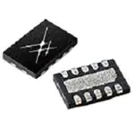
The SKY13322-375LF is a GaAs FET I/C single-pole, four-throw (SP4T) switch. This general purpose switch is an ideal choice for a variety of multiband telecommunication applications up to 6 GHz. The switch is manufactured in a compact, 2 x 3 mm, 10-pin exposed pad plastic Micro Leadframe Package Dual (MLPD) package. A functional block diagram is shown in Figure 1. The pin configuration and package are shown in Figure 2. Signal pin assignments and functional pin descriptions are provided in Table 1.
Features
Broadband frequency range: 0.1-6.0 GHz Low insertion loss: 0.45 dB @ 1 GHz Very high isolation: 28 dB @ 1 GHz Excellent linearity peformance: P1dB = +30 dBm @ 3.3 V Operating voltage range from 1.8 to 5.0 V Small, MLPD (10-pin, 2 x 3 mm) package (MSL1, 260 C per JEDEC J-STD-020)
J2
J4
J2 V2
1
10
J4 V4 RFC V3 J3
2
9
RFC
N/C V1
3
8
4
7
J1
J3
J1
5
6
S1537
S1538
Figure 1. SKY13322-375LF Block Diagram
Figure 2. SKY13322-375LF Pinout – 10-Pin MLPD (Top View)
Skyworks Solutions, Inc. • Phone [781] 376-3000 • Fax [781] 376-3100 • sales@skyworksinc.com • www.skyworksinc.com
201098C • Skyworks Proprietary Information • Products and Product Information are Subject to Change Without Notice • August 4, 2010 1
�DATA SHEET • SKY13322-375LF SP4T SWITCH
Table 1. SKY13322-375LF Signal Descriptions
Pin # 1 2 3 4 5 J2 V2 N/C V1 J1 Name Description RF output (Note 1) DC control voltage No connection DC control voltage RF output (Note 1) Pin # 6 7 8 9 10 J3 V3 RFC V4 J4 Name Description RF output (Note 1) DC control voltage RF common input (Note 1) DC control voltage RF output (Note 1)
Note 1: A 47 pF blocking capacitor is required for >1 GHz operation. Use larger value capacitors for lower frequency operation.
Table 2. SKY13322-375LF Absolute Maximum Ratings
Parameter Input power Voltage range Storage temperature Operating temperature
Note:
Symbol PIN VCTL TSTG TOP
Minimum
Typical +33 6
Maximum
Units dBm V C C
–65 –40
+150 +85
Exposure to maximum rating conditions for extended periods may reduce device reliability. There is no damage to device with only one parameter set at the limit and all other parameters set at or below their nominal value. Exceeding any of the limits listed here may result in permanent damage to the device.
CAUTION: Although this device is designed to be as robust as possible, Electrostatic Discharge (ESD) can damage this device. This device must be protected at all times from ESD. Static charges may easily produce potentials of several kilovolts on the human body or equipment, which can discharge without detection. Industry-standard ESD precautions should be used at all times.
Table 3. SKY13322-375LF Recommended Operating Conditions
Parameter Frequency Control voltage: Low High f VCTL_L VCTL_H Symbol Minimum 0.1 0 1.8 Typical Maximum 6.0 0.2 5.0 Units GHz V V
3.3
Electrical and Mechanical Specifications
The absolute maximum ratings of the SKY13322-375LF are provided in Table 2. The recommended operating conditions are specified in Table 3 and electrical specifications are provided in Table 4.
Typical performance characteristics of the SKY13322-375LF are illustrated in Figures 3 through 8. The state of the SKY13322-375LF is determined by the logic provided in Table 5.
Skyworks Solutions, Inc. • Phone [781] 376-3000 • Fax [781] 376-3100 • sales@skyworksinc.com • www.skyworksinc.com
2 August 4, 2010 • Skyworks Proprietary Information • Products and Product Information are Subject to Change Without Notice • 201098C
�DATA SHEET • SKY13322-375LF SP4T SWITCH
Table 4. SKY13322-375LF Electrical Specifications (Note 1) (VCTL = 0 V and +3.3 V, TOP = +25 C, PIN = 0 dBm, Characteristic Impedance [ZO] = 50 Ω, Unless Otherwise Noted)
Parameter Insertion loss IL Symbol Test Condition 0.1-1.0 GHz 1.0-2.5 GHz 2.5-3.0 GHz 3.0-4.0 GHz 4.0-6.0 GHz 0.1-1.0 GHz 1.0-2.5 GHz 2.5-3.0 GHz 3.0-4.0 GHz 4.0-6.0 GHz 0.1-1.0 GHz 1.0-2.5 GHz 2.5-3.0 GHz 3.0-4.0 GHz 4.0-6.0 GHz 10/90% or 90/10% RF 50% VCTL to 90/10% RF 26 23 23 23 15 15 15 10 Min Typical 0.45 0.60 0.75 1.00 2.00 28 26 27 27 18 22 22 22 13 7.5 60 60 40 IP1dB f = 0.9 GHz/2.45 GHz VCTL = 0 V/1.8 V, VCTL = 0 V/2.7 V VCTL = 0 V/3.3 V f = 48 MHz, VCTL = 0 V/2.7 V 0.1 dB Input Compression Point IP0.1dB f = 0.9 GHz/2.45 GHz VCTL = 0 V/1.8 V, VCTL = 0 V/2.7 V VCTL = 0 V/3.3 V f = 48 MHz, VCTL = 0 V/2.7 V Input IP3 IIP3 PIN = +15 dBm/tone, tone spacing = 1 MHz f = 0.9 GHz, f = 2.45 GHz 2nd harmonic 2fo PIN = +17 dBm f = 0.9 GHz f = 2.45 GHz 3rd harmonic 3fo PIN = +17 dBm f = 0.9 GHz f = 2.45 GHz Supply current ICC VCTL = 1.8 V to 5.0 V 70 65 5 dBc dBc μA 76 70 dBc dBc +54 +51 dBm dBm +17.5 +24.5 +27.0 +19.5 dBm dBm dBm dBm +21.0 +27.5 +30.0 +23.5 dBm dBm dBm dBm Max 0.60 0.75 0.95 1.25 Units dB dB dB dB dB dB dB dB dB dB dB dB dB dB dB ns ns mV
Isolation
Iso
Return loss (insertion loss state)
Switching characteristics: Rise/fall time On/off time Video feedthrough 1 dB Input Compression Point
Note 1: Performance is guaranteed only under the conditions listed in this Table.
Skyworks Solutions, Inc. • Phone [781] 376-3000 • Fax [781] 376-3100 • sales@skyworksinc.com • www.skyworksinc.com
201098C • Skyworks Proprietary Information • Products and Product Information are Subject to Change Without Notice • August 4, 2010 3
�DATA SHEET • SKY13322-375LF SP4T SWITCH
Typical Performance Characteristics
(VCTL = 0 V and +3.3 V, TOP = +25 C, PIN = 0 dBm, Characteristic Impedance [ZO] = 50 Ω, Blocking Capacitors = 47 pF, Unless Otherwise Noted)
0
0
–10
–0.5
–20
Insertion Loss (dB)
Isolation (dB)
–1.0
–30
–1.5
RFC to J1 RFC to J2 RFC to J3 RFC to J4
–40
–50 –60
–2.0
RFC to J2 RFC to J3 RFC to J4
–2.5 0 0.5 1.0 1.5 2.0 2.5 3.0 3.5 4.0 4.5 5.0 5.5 6.0
–70 0 0.5 1.0 1.5 2.0 2.5 3.0 3.5 4.0 4.5 5.0 5.5 6.0
Frequency (GHz)
Frequency (GHz)
Figure 3. Insertion Loss vs Frequency
Figure 4. Isolation vs Frequency (RFC to J1 Insertion Loss State)
0
0
–10
–10
–20
–20
Isolation (dB)
Isolation (dB)
–30
–30
–40
–40
–50 –60
RFC to J1 RFC to J3 RFC to J4
–50 –60
RFC to J1 RFC to J2 RFC to J4
–70 0 0.5 1.0 1.5 2.0 2.5 3.0 3.5 4.0 4.5 5.0 5.5 6.0
–70 0 0.5 1.0 1.5 2.0 2.5 3.0 3.5 4.0 4.5 5.0 5.5 6.0
Frequency (GHz)
Frequency (GHz)
Figure 5. Isolation vs Frequency (RFC to J2 Insertion Loss State)
Figure 6. Isolation vs Frequency (RFC to J3 Insertion Loss State)
0
0 –5
–10
–10 –15
–20
Return Loss (dB)
Isolation (dB)
–20 –25 –30 –35 –40 –45 –50
–30
–40
–50 –60
RFC to J1 RFC to J2 RFC to J3
RFC to J1 RFC to J2 RFC to J3 RFC to J4
–70 0 0.5 1.0 1.5 2.0 2.5 3.0 3.5 4.0 4.5 5.0 5.5 6.0
0
0.5
1.0
1.5
2.0
2.5
3.0
3.5
4.0
4.5
5.0
5.5
6.0
Frequency (GHz)
Frequency (GHz)
Figure 7. Isolation vs Frequency (RFC to J4 Insertion Loss State)
Figure 8. RFC Return Loss vs Frequency
Skyworks Solutions, Inc. • Phone [781] 376-3000 • Fax [781] 376-3100 • sales@skyworksinc.com • www.skyworksinc.com
4 August 4, 2010 • Skyworks Proprietary Information • Products and Product Information are Subject to Change Without Notice • 201098C
�DATA SHEET • SKY13322-375LF SP4T SWITCH
Table 5. SKY13322-375LF Truth Table
V1 (Pin 4) 1 0 0 0
Note:
V2 (Pin 2) 0 1 0 0
V3 (Pin 7) 0 0 1 0
V4 (Pin 9) 0 0 0 1
RFC to J1 Insertion loss Isolation Isolation Isolation
RFC to J2 Isolation Insertion loss Isolation Isolation
RFC to J3 Isolation Isolation Insertion loss Isolation
RFC to J4 Isolation Isolation Isolation Insertion loss
“1” = +1.8 V to +5 V. “0” = 0 V to +0.2 V. Any state other than described in this Table places the switch into an undefined state. An undefined state will not damage the device.
Evaluation Board Description
The SKY13322-375LF Evaluation Board is used to test the performance of the SKY13322-375LF SPDT Switch. An Evaluation Board schematic diagram is provided in Figure 9. An assembly drawing for the Evaluation Board is shown in Figure 10.
Package and Handling Information
Since the device package is sensitive to moisture absorption, it is baked and vacuum packed before shipping. Instructions on the shipping container label regarding exposure to moisture after the container seal is broken must be followed. Otherwise, problems related to moisture absorption may occur when the part is subjected to high temperature during solder assembly. THE SKY13322-375LF is rated to Moisture Sensitivity Level 1 (MSL1) at 260 C. It can be used for lead or lead-free soldering. Care must be taken when attaching this product, whether it is done manually or in a production solder reflow environment. Production quantities of this product are shipped in a standard tape and reel format.
Package Dimensions
The PCB layout footprint for the SKY13322-375LF is provided in Figure 11. Typical case markings are shown in Figure 12. Package dimensions for the 10-pin MLPD are shown in Figure 13, and tape and reel dimensions are provided in Figure 14.
CBL
1
10
CBL
RF Output DC Control Voltage (1.8-5.0 V)
×
2
J2 V2
3
J4
9
RF Output DC Control Voltage (1.8-5.0 V) RF Common Input DC Control Voltage (1.8-5.0 V) RF Output
V4
8
CBL
N/C
4
RFC
7
DC Control Voltage (1.8-5.0 V)
CBL
V1
5
V3
6
CBL
RF Output
J1
J3
CBL = 47 pF for >1 GHz operation. Exposed ground paddle should be grounded for best performance.
Use 10 nF blocking capacitors (CBL) for
很抱歉,暂时无法提供与“SKY13322-375LF”相匹配的价格&库存,您可以联系我们找货
免费人工找货- 国内价格 香港价格
- 1+23.050621+2.89060
- 10+17.1399110+2.14938
- 25+15.6659025+1.96454
- 100+14.04117100+1.76079
- 250+13.26685250+1.66369
- 500+12.80030500+1.60519
- 1000+12.416311000+1.55703


 工商网监
湘ICP备2023018690号
工商网监
湘ICP备2023018690号