DATA SHEET
SKY13412-487LF: 0.4 to 2.7 GHz SP12T Switch with GPIO
Interface
Applications
2G/3G/4G multimode cellular handsets (LTE, UMTS, CDMA2000,
EDGE, GSM)
Embedded data cards
TRX1
TRX2
TRX3
Features
TRX4
Broadband frequency range: 0.4 to 2.7 GHz
Low insertion loss
High isolation and linearity
Integrated GSM harmonic filter
Integrated GPIO interface
Ten TRX ports, one GSM low band transmit port, and one GSM
high band transmit port
Small QFN (30-pin, 3.0 x 3.8 x 0.75 mm) package (MSL1,
260 C per JEDEC J-STD-020)
TRX5
TRX6
ANT
TRX7
TRX8 (RX1)
TRX9 (RX2)
TRX10 (RX3)
TX1
TX2
V1
V2
V3
V4
Decoder
VDD
Skyworks Green™ products are compliant with
all applicable legislation and are halogen-free.
For additional information, refer to Skyworks
Definition of Green™, document number
SQ04-0074.
S2703
Figure 1. SKY13412-487LF Block Diagram
Description
The SKY13412-487LF is a single pole, twelve throw (SP12T)
antenna switch with integrated GSM transmit harmonic filter. The
SKY13412-487LF maintains a high linearity, high isolation, and
low insertion loss performance, which makes it an ideal choice for
UMTS, CDMA2000, EDGE, GSM, and LTE applications.
The design features two dedicated GSM transmit ports. The
remaining ten ports are suitable for WCDMA transmit/receive and
GSM receive functions. Three transmit ports have been
specifically designed to provide optimal LTE Band 13
performance. The switch exhibits an excellent triple beat ratio and
2nd/3rd order modulation distortion performance.
Switching is controlled by an integrated GPIO interface.
Depending on the logic applied to the decoder, the antenna pin is
connected to one of 12 switched RF ports using a low insertion
loss path, while the paths between the antenna pin and the other
RF pins are in a high isolation state. No external DC blocking
capacitors are required on the RF paths.
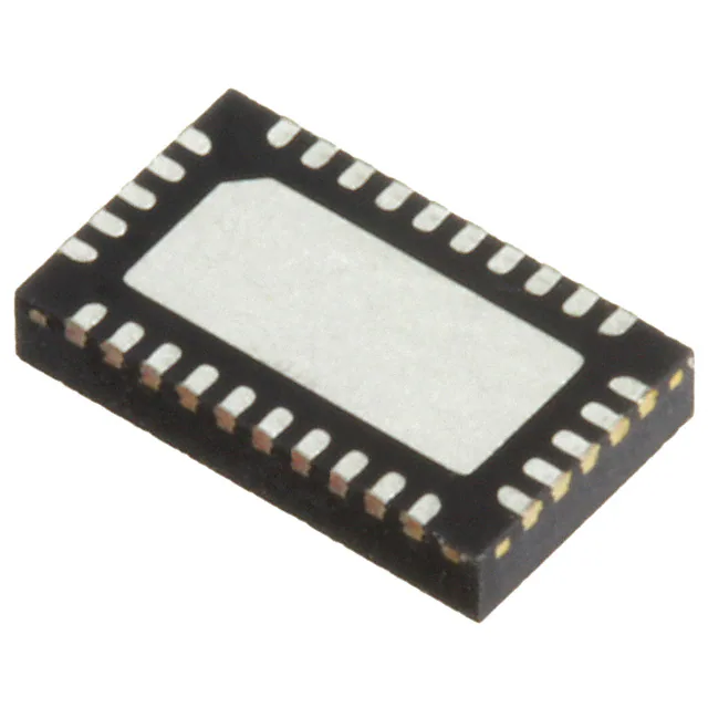
The SKY13412-487LF is manufactured in a compact,
3.0 x 3.8 x 0.75 mm, 30-pin surface mount Quad Flat No-Lead
(QFN) package.
A functional block diagram is shown in Figure 1. The pin
configuration and package are shown in Figure 2. Signal pin
assignments and functional pin descriptions are provided in
Table 1.
Skyworks Solutions, Inc. • Phone [781] 376-3000 • Fax [781] 376-3100 • sales@skyworksinc.com • www.skyworksinc.com
201762F • Skyworks Proprietary Information • Products and Product Information are Subject to Change Without Notice • September 18, 2014
1
�GND
V1
V2
V3
V4
VDD
DATA SHEET • SKY13412-487LF: SP12T SWITCH WITH GPIO INTERFACE
30
29
28
27
26
25
23
TRX2
TRX3
3
22
TRX1
TRX4
4
21
TRX7
TRX5
5
20
TRX8 (RX1)
TRX6
6
19
TRX9 (RX2)
GND
7
18
GND
ANT
8
17
TRX10 (RX3)
GND
9
16
GND
10
11
12
13
14
15
GND
2
TX1
GND
GND
GND
GND
24
TX2
1
GND
GND
S2810
Figure 2. SKY13412-487LF Pinout – 30-Pin QFN
(Top View)
Table 1. SKY13412-487LF Signal Descriptions (Note 1)
Pin
Name
Description
Pin
Name
Description
1
GND
Ground
16
GND
Ground
2
GND
Ground
17
TRX10 (RX3)
RF input/output port 10 (receive 3)
3
TRX3
RF input/output port 3. Optimized for LTE
Band 13 (704 to 787 MHz)
18
GND
Ground
4
TRX4
RF input/output port 4
19
TRX9 (RX2)
RF input/output port 9 (receive 2)
5
TRX5
RF input/output port 5
20
TRX8 (RX1)
RF input/output port 8 (receive 1)
6
TRX6
RF input/output port 6
21
TRX7
RF input/output port 7 optimized for LTE
Band 13 (704 to 787 MHz)
7
GND
Ground
22
TRX1
RF input/output port 1 optimized for LTE
Band 13 (704 to 787 MHz)
8
ANT
Antenna RF port
23
TRX2
RF input/output port 2
9
GND
Ground
24
GND
Ground
10
GND
Ground
25
VDD
DC power supply
11
TX2
GSM high band transmit RF input port with
integrated harmonic filter
26
V4
DC input control voltage 4
12
GND
Ground
27
V3
DC input control voltage 3
13
GND
Ground
28
V2
DC input control voltage 2
14
TX1
GSM low band transmit RF input port with
integrated harmonic filter
29
V1
DC input control voltage 1
15
GND
Ground
30
GND
Ground
Note 1: Bottom ground paddles must be connected to ground.
Skyworks Solutions, Inc. • Phone [781] 376-3000 • Fax [781] 376-3100 • sales@skyworksinc.com • www.skyworksinc.com
2
September 18, 2014 • Skyworks Proprietary Information • Products and Product Information are Subject to Change Without Notice • 201762F
�DATA SHEET • SKY13412-487LF: SP12T SWITCH WITH GPIO INTERFACE
Electrical and Mechanical Specifications
+20 dBm Continuous Wave (CW) signal, fFUND, is sequentially
applied to the TRX1 through TRX8 ports, while a –15 dBm CW
blocker signal, fBLK, is applied to the ANT port.
The absolute maximum ratings of the SKY13412-487LF are
provided in Table 2. Electrical specifications are provided in
Tables 3 through 8. Table 9 provides the control logic for the
SKY13412-487LF.
The resulting 3rd Order Intermodulation Distortion (IMD3), fRX, is
measured over all phases of fFUND. The SKY13412-487LF exhibits
exceptional performance for all TRXx ports.
Figure 3 illustrates the test setup used to measure
intermodulation products. This industry standardized test is used
to simulate the WCDMA Band 1 linearity of the antenna switch. A
Table 2. SKY13412-487LF Absolute Maximum Ratings (Note 1)
Parameter
Minimum
Maximum
Units
VDD
2.5
5.0
V
Digital control signals (V1, V2, V3, V4)
VCTRL
–0.5
+3.5
V
RF input power:
TX1 pin
TX2 pin
All TRXx pins (Note 2)
PIN
+36
+34
+33
dBm
dBm
dBm
Storage temperature
TSTG
–55
+150
C
Operating temperature
TOP
–35
+90
C
Power supply
Symbol
Note 1: Exposure to maximum rating conditions for extended periods may reduce device reliability. There is no damage to device with only one parameter set at the limit and all other
parameters set at or below their nominal value. Exceeding any of the limits listed here may result in permanent damage to the device.
Note 2: All TRXx ports absolute maximum power are evaluated with GSM modulated signal at 50 Ω matching condition.
CAUTION: Although this device is designed to be as robust as possible, electrostatic discharge (ESD) can damage this device. This device
must be protected at all times from ESD. Static charges may easily produce potentials of several kilovolts on the human body
or equipment, which can discharge without detection. Industry-standard ESD precautions should be used at all times.
Table 3. SKY13412-487LF Electrical Specifications (Note 1) (1 of 3)
(VDD = 2.85 V, TOP = +25 C, Characteristic Impedance [ZO] = 50 Ω, Unless Otherwise Noted)
Parameter
Symbol
Test Condition
Min
Typical
Max
Units
RF Specifications
Insertion loss
IL
Transmit low band, 915 MHz
1.10
1.45
dB
Transmit high band, 1910 MHz
1.10
1.40
dB
TRX1/3/7 Band 13, 704 to 787 MHz
0.40
0.60
dB
TRXx ports, 960 MHz, +26 dBm
0.50
0.70
dB
TRXx ports, 1990 MHz, +26 dBm
0.60
0.80
dB
TRXx ports, 2170 MHz, +26 dBm
0.70
0.90
dB
TRXx ports, 2690 MHz
0.95
1.15
dB
Skyworks Solutions, Inc. • Phone [781] 376-3000 • Fax [781] 376-3100 • sales@skyworksinc.com • www.skyworksinc.com
201762F • Skyworks Proprietary Information • Products and Product Information are Subject to Change Without Notice • September 18, 2014
3
�DATA SHEET • SKY13412-487LF: SP12T SWITCH WITH GPIO INTERFACE
Table 3. SKY13412-487LF Electrical Specifications (Note 1) (2 of 3)
(VDD = 2.85 V, TOP = +25 C, Characteristic Impedance [ZO] = 50 Ω, Unless Otherwise Noted)
Parameter
Symbol
Test Condition
Min
Typical
Max
Units
Transmit low band to ANT,
2fo 1648 to 1830 MHz
28
25
dB
Transmit low band to ANT,
3fo 2472 to 2745 MHz
28
25
dB
Transmit low band to ANT,
2fo 3296 to 3660 MHz
25
18
dB
Transmit high band to ANT,
2fo 3420 to 3820 MHz
28
25
dB
Transmit high band to ANT,
3fo 5130 to 5730 MHz
28
25
dB
Transmit GSM low band,
PIN


 工商网监
湘ICP备2023018690号
工商网监
湘ICP备2023018690号
