DATA SHEET
SKY14151-350LF: 20 MHz-2.5 GHz High Power SP4T Switch
With Decoder
Applications
GSM/WCDMA/EDGE datacards and handsets
Mobile high power switching systems
RF1
RF2
ANT
RF3
Features
Broadband frequency range: 20 MHz to 2.5 GHz
Low insertion loss: 0.40 dB @ 1 GHz, 0.45 dB @ 2 GHz with
high isolation (29 dB @ 1 GHz)
VDD: 2.5 to 3.0 V for high power applications; can be used down
to 1.8 V for low power applications
High linearity IMD < –111 dBm over phase
Good harmonic performance < –80 dBc @ 0.9 GHz
Low voltage logic compatible (minimum VHIGH = 1.8 V)
Small, QFN (16-pin, 3 x 3 mm) package (MSL1, 260 C per
JEDEC J-STD-020)
RF4
CTRL1
CTRL2
S1947
Figure 1. SKY14151-350LF Block Diagram
Description
The SKY14151-350LF is a symmetrical, single-pole, four-throw
(SP4T) switch. The device is designed for broadband, high power
switching applications that demand high linearity and low
insertion loss. This is a general purpose switch optimized for a
variety of multimode applications such as GSM/WCDMA/EDGE.
The switch is manufactured using Skyworks state-of-the-art
pHEMT process. The SKY14151-350LF features integrated logic
that uses only two control lines for switch operation. The low
current consumption makes the device suitable for batteryoperated applications.
N/C
RF2
GND
RF1
The SKY14151-350LF SP4T switch is provided in a compact Quad
Flat No-Lead (QFN) 3 x 3 mm package. A functional block
diagram is shown in Figure 1. The pin configuration and package
are shown in Figure 2. Signal pin assignments and functional pin
descriptions are provided in Table 1.
16
15
14
13
VDD
2
11
ANT
CTRL2
3
10
GND
CTRL1
4
9
GND
5
6
7
8
RF3
GND
GND
12
RF4
1
GND
GND
S1948
Figure 2. SKY14151-350LF Pinout – 16-Pin QFN
(Top View)
Skyworks Solutions, Inc. • Phone [781] 376-3000 • Fax [781] 376-3100 • sales@skyworksinc.com • www.skyworksinc.com
200983H • Skyworks Proprietary Information • Products and Product Information are Subject to Change Without Notice • October 6, 2010
1
�DATA SHEET • SKY14151-350LF SP4T SWITCH
Table 1. SKY14151-350LF Signal Descriptions
Pin #
Name
Description
Pin #
Name
Description
1
GND
Ground
9
GND
Ground
2
VDD
Supply voltage input. The voltage may be
switched. The switching time must be no longer
than the start-up time.
10
GND
Ground
3
CTRL2
Control signal 2. The logic level applied to this
pin, along with the logic level applied to pin 4,
controls the state of the switch.
11
ANT
Antenna. This pin is connected directly and
exclusively to pin 6, 8, 13, or 15 depending on
the control voltage applied to pins 3 and 4. A DC
blocking capacitor is required.
4
CTRL1
Control signal 1. The logic level applied to this
pin, along with the logic level applied to pin 3,
controls the state of the switch.
12
GND
Ground
5
GND
Ground
13
RF1
RF output 1. This pin is either connected directly
to or is disconnected from pin 11, depending on
the control voltage applied to pins 3 and 4. A DC
blocking capacitor is required.
6
RF4
RF output 4. This pin is either connected directly
to or is disconnected from pin 11, depending on
the control voltage applied to pins 3 and 4. A DC
blocking capacitor is required.
14
GND
Ground
7
GND
Ground
15
RF2
RF output 2. This pin is either connected directly
to or is disconnected from pin 11, depending on
the control voltage applied to pins 3 and 4. A DC
blocking capacitor is required.
8
RF3
RF output 3. This pin is either connected directly
to or is disconnected from pin 11, depending on
the control voltage applied to pins 3 and 4. A DC
blocking capacitor is required.
16
N/C
No connection.
Table 2. SKY14151-350LF Absolute Maximum Ratings
Maximum
Units
Supply voltage
Parameter
VDD
Symbol
Minimum
3
V
Input power (20 MHz to 2.5 GHz,
VDD = 2.5 to 3.0 V)
PIN
+36
dBm
Control voltage
CTRL1, CTRL2
3
V
Operating temperature
TOP
–40
+85
C
Storage temperature
TSTG
–50
+100
C
Note:
Exposure to maximum rating conditions for extended periods may reduce device reliability. There is no damage to device with only one parameter set at the limit and all other
parameters set at or below their nominal value. Exceeding any of the limits listed here may result in permanent damage to the device.
CAUTION: Although this device is designed to be as robust as possible, Electrostatic Discharge (ESD) can damage this device. This device
must be protected at all times from ESD. Static charges may easily produce potentials of several kilovolts on the human body
or equipment, which can discharge without detection. Industry-standard ESD precautions should be used at all times.
Skyworks Solutions, Inc. • Phone [781] 376-3000 • Fax [781] 376-3100 • sales@skyworksinc.com • www.skyworksinc.com
2
October 6, 2010 • Skyworks Proprietary Information • Products and Product Information are Subject to Change Without Notice • 200983H
�DATA SHEET • SKY14151-350LF SP4T SWITCH
Functional Description
The SKY14151-350LF is comprised of a CMOS decoder that
enables two TTL-compatible DC lines to control four RF ports. The
decoder is internally connected to a GaAs pHEMT RF switch.
Depending on the logic voltage level applied to the control pins,
the ANT pin is connected to one of four switched RF outputs (RF1,
RF2, RF3, or RF4) by a low insertion loss path, while maintaining
a high isolation path to the alternate port.
When VDD is not applied, the device is considered off or inactive.
All arms of the switch remain on in this state, creating a poor
four-way power splitter. The return loss of all RF ports is very low
in this state. RF should not be applied when VDD is not present
and should only be used to conserve current.
Electrical and Mechanical Specifications
Startup time is defined as the time from when VDD is applied to
when the switch is active. Once the startup time has passed, the
control voltages CTRL1 and CTRL2 can be applied. RF power
should not be applied during the startup time or damage to the
device could result.
The absolute maximum ratings of the SKY14151-350LF are
provided in Table 2. Electrical specifications are provided in
Table 3.
The recommended startup sequence is:
Typical performance characteristics of the SKY14151-350LF are
illustrated in Figures 3 through 10.
Step 1: Apply VDD.
The state of the SKY14151-350LF is determined by the logic
provided in Table 4.
Figure 11 illustrates the test setup used to measure data for 3rd
Order Intermodulation Distortion (IMD3) testing. Figure 12
illustrates the test setup used to measure triple beat ratio data.
Step 2: Apply CTRL1 and CTRL2
Step 3: Apply RF input.
The device must be turned off in the reverse order.
Table 3. SKY14151-350LF Electrical Specifications (1 of 3) (Note 1)
(VDD = 2.65 V, CTRL1 = CTRL2 = VDD, TOP = +25 C, All Unused RF Ports are Terminated in a 50 Ω Load, Unless Otherwise Noted)
Parameter
Symbol
Test Condition
Min
Typical
Max
Units
0.40
0.45
0.50
0.50
0.60
0.60
dB
dB
dB
RF Specifications
Insertion loss
IL
0.02 to 1.0 GHz
1.0 to 2.0 GHz
2.0 to 2.1 GHz
Isolation
ISO
0.02 to 1.0 GHz
1.0 to 2.0 GHz
2.0 to 2.1 GHz
Return loss
|S11|
0.02 to 2.5 GHz, all RF
ports, insertion loss state
Second harmonic
2fo
fFUND = 900 MHz,
PIN = +34.5 dBm
Third harmonic
3fo
29
24
23
dB
dB
dB
15
dB
–75
–80
dBc
fFUND = 0.12 GHz,
PIN = +10 dBm
–75
–80
dBc
fFUND = 0.4 GHz,
PIN = +10 dBm
–80
–90
dBc
fFUND = 1.8 GHz,
PIN = +31.5 dBm
–70
–85
dBc
fFUND = 900 MHz,
PIN = +34.5 dBm
–70
–80
dBc
fFUND = 0.12 GHz,
PIN = +10 dBm
–80
–90
dBc
fFUND = 0.4 GHz,
PIN = +10 dBm
–80
–90
dBc
fFUND = 1.8 GHz,
PIN = +31.5 dBm
–70
–80
dBc
26
19
19
Skyworks Solutions, Inc. • Phone [781] 376-3000 • Fax [781] 376-3100 • sales@skyworksinc.com • www.skyworksinc.com
200983H • Skyworks Proprietary Information • Products and Product Information are Subject to Change Without Notice • October 6, 2010
3
�DATA SHEET • SKY14151-350LF SP4T SWITCH
Table 3. SKY14151-350LF Electrical Specifications (2 of 3) (Note 1)
(VDD = 2.65 V, CTRL1 = CTRL2 = VDD, TOP = +25 C, All Unused RF Ports are Terminated in a 50 Ω Load, Unless Otherwise Noted)
Parameter
Symbol
Test Condition
Min
Typical
Max
Units
+37.0
+34.0
+38.5
+38.0
+35.0
dBm
dBm
dBm
fFUND = 1.95 GHz @
+20 dBm,
fBLK = 1.76 GHz
@ –15 dBm,
fRX = 2.14 GHz, worst
case over phase. See
Figure 9.
–111
dBm
@ 900 MHz, VSWR = 20:1
@ 1.8 GHz, VSWR = 20:1
+34.5
+31.5
dBm
dBm
f0 = 836.61 MHz
@ +26 dBm,
f2 = 1718.22 MHz
@ –20 dBm, measured
@ 881.61 MHz
+113.5
dBm
RF Specifications (continued)
Input 0.1 dB compression point
3rd Order Intermodulation Distortion
P0.1dB
IMD3
Power handling under mismatch
2nd Order Input Intercept Point
IIP2
@ 48 MHz
@ 900 MHz
@ 1.8 GHz
Switching speed
10/90% RF rise/fall time
5
μs
Startup time
Wait time required from
when VDD is applied until
control voltage can be
applied
25
μs
Triple beat ratio (matched)
3BR
f1 = 1880 MHz,
P1 = +21.5 dBm,
f2 = 1881 MHz,
P2 = +21.5 dBm,
fJAMMER = 1960 MHz,
PJAMMER = –30 dBm,
measured @ 1959 MHz
and 1961 MHz for worst
case, 50 Ω load
+81
+82
dBc
f1 = 891.025 MHz
@ +14 dBm,
f2 = 892.025 MHz,
P2 = +14 dBm,
fJAMMER = 836.0125 MHz,
PJAMMER = –30 dBm,
measured @
835.0125 MHz and
837.0125 MHz for worst
case, 50 Ω load
+81
+82
dBc
f1 = 825.995 MHz,
P1 = +21.5 dBm,
f2 = 826.995 MHz,
P2 = +21.5 dBm,
fJAMMER = 870.995 MHz,
PJAMMER = –30 dBm,
measured @
869.995 MHz and
871.995 MHz for worst
case, 50 Ω load
+81
+82
dBc
Skyworks Solutions, Inc. • Phone [781] 376-3000 • Fax [781] 376-3100 • sales@skyworksinc.com • www.skyworksinc.com
4
October 6, 2010 • Skyworks Proprietary Information • Products and Product Information are Subject to Change Without Notice • 200983H
�DATA SHEET • SKY14151-350LF SP4T SWITCH
Table 3. SKY14151-350LF Electrical Specifications (3 of 3) (Note 1)
(VDD = 2.65 V, CTRL1 = CTRL2 = VDD, TOP = +25 C, All Unused RF Ports are Terminated in a 50 Ω Load, Unless Otherwise Noted)
Parameter
Symbol
Test Condition
Min
Typical
Max
Units
f1 = 1880 MHz,
P1 = +21.5 dBm,
f2 = 1881 MHz,
P2 = +21.5 dBm,
fJAMMER = 1960 MHz,
PJAMMER = –30 dBm,
measured @ 1959 MHz
and 1961 MHz for worst
case over phase, 2:1
VSWR load
+81
+82
dBc
f1 = 891.025 MHz,
P1 = +14 dBm,
f2 = 892.025 MHz,
P2 = +14 dBm,
fJAMMER = 836.0125 MHz,
PJAMMER = –30 dBm,
measured @
835.0125 MHz and
837.0125 MHz for worst
case over phase, 2:1
VSWR load
+81
+82
dBc
f1 = 825.995 MHz,
P1 = +21.5 dBm,
f2 = 826.995 MHz,
P2 = +21.5 dBm,
fJAMMER = 870.995 MHz,
PJAMMER = –30 dBm,
measured @
869.995 MHz and
871.995 MHz for worst
case over phase, 2:1
VSWR load
+81
+82
dBc
1.8
2.0
RF Specifications (continued)
Triple beat ratio (2:1 VSWR)
3BR
DC/Control Specifications
Switched supply voltage (Note 2)
VDD
Switched supply current
IDD
Control voltage:
High
Low
CTRL1, CTRL2
Control current:
High
Low
ICTL
3.00
0.3
1.80 (Note 3)
2.65
0
V
mA
3.00
0.3
0.5
0.5
V
V
μA
μA
Note 1: Performance is guaranteed only under the conditions listed in this Table.
Note 2: For best receiver sensitivity, VDD is recommended to be between 1.8 and 2.0 V with CTRL1/2 (high) no larger than VDD.
Note 3: For 1.8 V control, VDD must be ≤ 2.65 V.
Skyworks Solutions, Inc. • Phone [781] 376-3000 • Fax [781] 376-3100 • sales@skyworksinc.com • www.skyworksinc.com
200983H • Skyworks Proprietary Information • Products and Product Information are Subject to Change Without Notice • October 6, 2010
5
�DATA SHEET • SKY14151-350LF SP4T SWITCH
Table 4. SKY14151-350LF Truth Table
Note:
State
CTRL1 (Pin 4)
CTRL2 (Pin 3)
RF Path
1
VLOW
VLOW
ANT to RF1
2
VLOW
VHIGH
ANT to RF2
3
VHIGH
VLOW
ANT to RF3
4
VHIGH
VHIGH
ANT to RF4
VHIGH = 1.8 V to VDD
VLOW = 0 to 0.3 V
Any state other than described in this Table places the switch into an undefined state.
Typical Performance Characteristics
(VDD = 2.5 to 3.0 V, CTRL1 = CTRL2 = VDD, TOP = +25 C, All Unused RF Ports are Terminated in a 50 Ω Load, Unless Otherwise Noted)
0
0
RF1
RF2
RF3
RF4
–0.1
ANT to RF2
ANT to RF3
ANT to RF4
–10
–0.3
Isolation (dB)
Insertion Loss (dB)
–0.2
–5
–0.4
–0.5
–0.6
–15
–20
–25
–0.7
–30
–0.8
–35
–0.9
–1.0
0.5
1.0
1.5
2.0
2.5
–40
3.0
0.5
1.0
Frequency (GHz)
–15
Isolation (dB)
Isolation (dB)
–10
–15
–20
–25
–20
–25
–30
–30
–35
–35
2.0
Frequency (GHz)
Figure 5. Isolation vs Frequency
(ANT to RF2 Insertion Loss State)
2.5
ANT to RF1
ANT to RF2
ANT to RF4
–5
–10
1.5
3.0
–40
0.5
1.0
1.5
2.0
Frequency (GHz)
Figure 6. Isolation vs Frequency
(ANT to RF3 Insertion Loss State)
Skyworks Solutions, Inc. • Phone [781] 376-3000 • Fax [781] 376-3100 • sales@skyworksinc.com • www.skyworksinc.com
6
3.0
0
ANT to RF1
ANT to RF3
ANT to RF4
–5
1.0
2.5
Figure 4. Isolation vs Frequency
(ANT to RF1 Insertion Loss State)
0
0.5
2.0
Frequency (GHz)
Figure 3. Insertion Loss vs Frequency
–40
1.5
October 6, 2010 • Skyworks Proprietary Information • Products and Product Information are Subject to Change Without Notice • 200983H
2.5
3.0
�DATA SHEET • SKY14151-350LF SP4T SWITCH
0
0
ANT to RF1
ANT to RF2
ANT to RF3
–5
Input Return Loss (dB)
Isolation (dB)
–10
–15
–20
–25
–30
–10
–15
–20
–25
–30
–35
–35
–40
RF1
RF2
RF3
RF4
–5
–40
0.5
1.0
1.5
2.0
2.5
0.5
3.0
1.0
1.5
2.0
2.5
3.0
Frequency (GHz)
Frequency (GHz)
Figure 8. Input Return Loss vs Frequency
Figure 7. Isolation vs Frequency
(ANT to RF4 Insertion Loss State)
–100
+5
–105
Noise Figure (dB)
+4
IMD3 (dBm)
–110
–115
–120
+3
+2
+1
0
–125
–1
0.6
0.8
1.0
1.2
1.4
1.6
1.8
2.0
2.2
Frequency (GHz)
–130
0
20
40
60
80
100
120
140
160
180
Note: For best receiver sensitivity, VDD is recommended to be between 1.8 and 2.0 V
with CTRL1/2 (high) no larger than VDD.
Phase (deg)
Figure 10. Typical Noise Figure vs Frequency
(VDD = 2 V, CTRL1/2 = 1.8 V)
Figure 9. 3rd Order Intermodulation Distortion vs Phase
fBLK
1760 MHz
@ –15 dBm
fFUND
1950 MHz
@ +20 dBm
fRX
2140 MHz,
Measure Tone
Circulator
Signal Generator
fFUND = 1950 MHz,
@ +20 dBm
Coupler to Monitor
Input Power
1950 MHz
Bandpass Filter
Circulator
Duplexer
Phase Shifter
SKY14151-350LF
PFUND = +20 dBm
PBLK = –15 dBm
1760 MHz
Bandpass Filter
Signal Generator
fBLK = 1760 MHz
@ –15 dBm
Spectrum Analyzer
fRX = 2140 MHz
S1909a
Figure 11. 3rd Order Intermodulation Test Setup
Skyworks Solutions, Inc. • Phone [781] 376-3000 • Fax [781] 376-3100 • sales@skyworksinc.com • www.skyworksinc.com
200983H • Skyworks Proprietary Information • Products and Product Information are Subject to Change Without Notice • October 6, 2010
7
�DATA SHEET • SKY14151-350LF SP4T SWITCH
Circulator
LPF
Testing under mismatched conditions over phase
or
testing under matched conditions: ZL = 50 Ω
Combiner
f1
PIN1, PIN2,
PINJAMMER
Circulator
f1, f2
Phase Shifter
Directional Coupler
LPF
SKY14151-350LF
f2
10 dB
10 dB
fJAMMER
fJAMMER
P
10 dB
ZL
Spectrum
Analyzer
10 dB
30 dB
Circulator
f
P3BL, P3BH
fJAMMER
Power Meter
P (dBm)
3BRL = PJAMMER – P3BL
3BRH = PJAMMER – P3BH
3BR = Min(3BRL, 3BRH)
PJAMMER
P3BL
f3BL = fJAMMER – (f2 – f1)
P3BH
fJAMMER
f3BH = fJAMMER + (f2 – f1)
f
S1972
Figure 12. Triple Beat Ratio (3BR) Test Setup
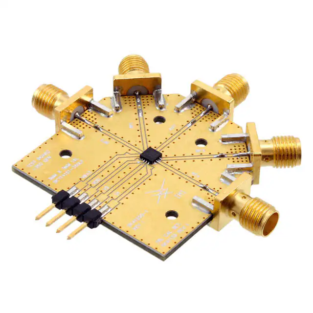
Evaluation Board Description
The SKY14151-350LF Evaluation Board is used to test the
performance of the SKY14151-350LF SP4T Switch. An Evaluation
Board schematic diagram is provided in Figure 13. An assembly
drawing for the Evaluation Board is shown in Figure 14.
Components C3 and L1 constitute an ESD filter. This topology and
the component values noted in Figure 13 may vary according to
the ESD requirement and acceptable insertion loss for a specific
application.
Decoupling capacitors (C3 through C6) are recommended to
suppress noise and to prevent RF leakage into the DC control
circuits.
DC blocking capacitors C1, C2, C7, C8, and C9 determine the low
frequency operation of the switch. Increase the capacitor values
to lower operation frequency.
Skyworks Solutions, Inc. • Phone [781] 376-3000 • Fax [781] 376-3100 • sales@skyworksinc.com • www.skyworksinc.com
8
October 6, 2010 • Skyworks Proprietary Information • Products and Product Information are Subject to Change Without Notice • 200983H
�DATA SHEET • SKY14151-350LF SP4T SWITCH
RF Output 2
RF Output 4
×
C2
100 pF
13
RF1
14
GND
15
N/C
16
RF2
C1
100 pF
1
GND
GND
VDD
ANT
2
Supply Voltage
C4
10 nF
3
Control Signal 2
C5
100 pF
4
CTRL2
GND
CTRL1
GND
12
C3
1 pF
L1
10 nH
11
10
Antenna
C9
100 pF
9
5
6
7
RF3
RF4
GND
C6
100 pF
GND
Control Signal 1
8
RF Output 4
RF Output 3
C7
100 pF
C8
100 pF
Note: Some component labels may be different than the
corresponding component symbol shown here.
Component values, however, are accurate as of the
date of this Data Sheet.
S1950
Use 10 nF DC blocking capacitors (C1, C2, C7, C8,
and C9) for


 工商网监
湘ICP备2023018690号
工商网监
湘ICP备2023018690号
