DATA SHEET
SKY65095-360LF: 1600 to 2100 MHz Low-Noise Power
Amplifier Driver
Applications
2.5G, 3G, 4G wireless infrastructure transceivers
ISM band transmitters
WCS fixed wireless
Active Bias
3GPP LTE
RF_IN
RF_OUT/BIAS
Features
Wideband frequency range: 1600 to 2100 MHz
GND
ENABLE
Low noise figure: 4.5 dB
High IIP3 up to +32 dBm
Output P1dB = +28.5 dBm
S1964a
Figure 1. SKY65095-360LF Functional Block Diagram
High gain: +14.5 dBm
Single DC supply: +5 V
Description
Enable voltage: +3.3 V
The Skyworks SKY65095-360LF is a high-performance,
ultra-wideband power amplifier (PA) driver with superior output
power, low noise, and linearity. The device provides excellent
noise figure (NF) and high output power at 1 dB compression,
which makes the SKY65095-360LF ideal for use in the driver
stage of infrastructure transmit or receive chains.
On-chip bias circuit
DFN (8-pin, 2 x 2 mm) package
(MSL1, 260 °C per JEDEC J-STD-020)
TM
Skyworks Green products are compliant with
all applicable legislation and are halogen-free.
For additional information, refer to Skyworks
Definition of GreenTM, document number
SQ04–0074.
GND
1
8
N/U
RF_IN
2
7
RF_OUT/BIAS
N/U
3
6
ENABLE
N/U
4
5
N/U
The SKY65095-360LF uses low-cost surface-mount technology
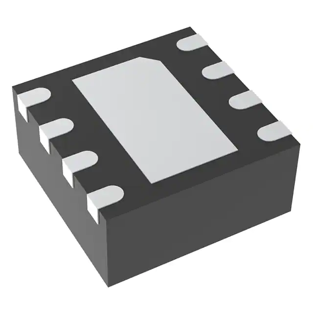
(SMT) in the form of an 8-pin, 2 x 2 mm Dual Flat No-Lead (DFN)
package. A functional block diagram is provided in Figure 1, and
the device package and pinout are shown in Figure 2. Signal pin
assignments and functional pin descriptions are described in
Table 1.
S2494
Figure 2. SKY65095-360LF Pinout
(Top View)
Skyworks Solutions, Inc. • Phone [781] 376-3000 • Fax [781] 376-3100 • sales@skyworksinc.com • www.skyworksinc.com
201569D • Skyworks Proprietary Information • Products and Product Information are Subject to Change Without Notice • September 13, 2017
1
�DATA SHEET • SKY65095-360LF: 1600 TO 2100 MHz LOW-NOISE POWER AMPLIFIER DRIVER
Table 1. SKY65095-360LF Signal Descriptions
Pin
Name
Description
Pin
Name
Description
1
GND
Ground
5
N/U
Not used (may be grounded)
2
RF_IN
RF input
6
ENABLE
PA enable
3
N/U
Not used (may be grounded)
7
RF_OUT/BIAS
RF output/bias voltage
4
N/U
Not used (may be grounded)
8
N/U
Not used (may be grounded)
Technical Description
Electrical and Mechanical Specifications
The SKY65095-360LF is a single-stage, low-noise PA that
operates with a single 5 V power supply connected through an RF
choke (inductor L1) to the output signal (pin 7). The bias current is
set by the on-chip active bias composed of current mirror and
reference voltage transistors, which allow excellent gain tracking
over temperature and voltage variations. The device is externally
RF matched using surface-mount components to facilitate
operation over a frequency range of 1600 to 2100 MHz.
The absolute maximum ratings of the SKY65095-360LF are
provided in Table 2. The recommended operating conditions are
specified in Table 3 and electrical specifications are provided in
Table 4 (general specifications), Table 5 (1626 to 1660 MHz),
Table 6 (1710 to 1780 MHz), Table 7 (1850 to 1910 MHz), Table 8
(1920 to 1980 MHz), and Table 9 (2010 to 2025 MHz).
Typical performance characteristics of the SKY65095-360LF are
illustrated in Figures 3 through 13 (1626 to 1660 MHz), Figures
14 through 24 (1710 to 1785 MHz), Figures 25 through 44 (1850
to 1910 MHz), Figures 45 through 55 (1920 to 1980 MHz), and
Figures 56 through 66 (2010 to 2025 MHz).
Table 2. SKY65095-360LF Absolute Maximum Ratings1
Parameter
Symbol
Minimum
Maximum
Units
–0.3
+6.0
V
Supply voltage
VCC
RF input power
PIN
+20
dBm
Supply current @ P1dB
ICC
400
mA
Power dissipation @ P1dB
PD
1.1
W
Power dissipation @ PIN = –10 dBm
PD
Operating case temperature
TC
0
0.7
W
+70
°C
Extended operating temperature
TEXT
–33
+95
°C
Storage temperature
TST
–55
+150
°C
Junction temperature @ PIN = –10 dBm
TJ
+150
°C
Thermal resistance @ PIN = –10 dBm
ΘJC
35
°C/W
1 Exposure to maximum rating conditions for extended periods may reduce device reliability. There is no damage to device with only one parameter set at the limit and all other parameters set
at or below their nominal values. Exceeding any of the limits listed here may result in permanent damage to the device.
ESD HANDLING: Although this device is designed to be as robust as possible, electrostatic discharge (ESD) can damage this device.
This device must be protected at all times from ESD when handling or transporting. Static charges may easily produce
potentials of several kilovolts on the human body or equipment, which can discharge without detection.
Industry-standard ESD handling precautions should be used at all times.
Skyworks Solutions, Inc. • Phone [781] 376-3000 • Fax [781] 376-3100 • sales@skyworksinc.com • www.skyworksinc.com
2
September 13, 2017 • Skyworks Proprietary Information • Products and Product Information are Subject to Change Without Notice • 201569D
�DATA SHEET • SKY65095-360LF: 1600 TO 2100 MHz LOW-NOISE POWER AMPLIFIER DRIVER
Table 3. SKY65095-360LF Recommended Operating Conditions
Parameter
Symbol
Bias voltage
VCC
Enable voltage
VEN
Operating frequency
f
Min
Typ
Max
4.75
5.00
5.25
Units
V
3.3
V
1600
2100
MHz
Table 4. SKY65095-360LF Electrical Characteristics: General Specifications1
(VCC = +5 V, TJ = 25 °C, CW, Unless Otherwise Noted)
Parameter
Quiescent current
Symbol
IQ
Test Conditions
No RF
Gain vs temperature
0.1 dB output compression point
Min
Typical
135
–0.02
OP0.1dB
Sweep input power
Turn-on time
PIN = –10 dBm,
VEN = 3.3 V
Stability
PIN = 0 dBm, TJ = 0 °C
Max
Units
145
mA
+0.02
dB/°C
+22
dBm
1
μs
Unconditional
–
1 Performance is guaranteed only under the conditions listed in this table, and corresponds to the Bill of Materials in Table 10 for each frequency band.
Table 5. SKY65095-360LF Electrical Characteristics: 1626 to 1660 MHz1
(VCC = +5 V, TJ = 25 °C, f = 1643 MHz, CW, Unless Otherwise Noted)
Parameter
Symbol
Test Conditions
Frequency
f
Third order input intercept point
IIP3
PIN = –10 dBm/tone,
5 MHz spacing
Small signal gain
|S21|
PIN = –30 dBm
Input return loss
|S11|
Output return loss
|S22|
Noise figure
NF
1 dB output compression point
OP1dB
Min
Typ
1626
Max
Units
1660
MHz
+29.5
dBm
15.0
dB
PIN = –30 dBm
25
dB
PIN = –30 dBm
7.5
dB
4.5
dB
+27.5
dBm
Sweep input power
1 Performance is verified by characterization. Evaluation Board input trace loss up to DC blocking capacitors = 0.16 dB. Output trace loss up to DC blocking capacitors = 0.16 dB.
Table 6. SKY65095-360LF Electrical Characteristics: 1710 to 1785 MHz1
(VCC = +5 V, TJ = 25 °C, f = 1747.5 MHz, CW, Unless Otherwise Noted)
Parameter
Symbol
Test Conditions
Frequency
f
Third order input intercept point
IIP3
PIN = –10 dBm/tone,
5 MHz spacing
Small signal gain
|S21|
Input return loss
Output return loss
Min
Typ
1710
Max
Units
1785
MHz
+29.5
dBm
PIN = –30 dBm
14.5
dB
|S11|
PIN = –30 dBm
25.5
dB
|S22|
PIN = –30 dBm
8.2
dB
Noise figure
NF
1 dB output compression point
OP1dB
Sweep input power
4.5
dB
+27.2
dBm
1 Performance is verified by characterization. Evaluation Board input trace loss up to DC blocking capacitors = 0.17 dB. Output trace loss up to DC blocking capacitors = 0.17 dB.
Skyworks Solutions, Inc. • Phone [781] 376-3000 • Fax [781] 376-3100 • sales@skyworksinc.com • www.skyworksinc.com
201569D • Skyworks Proprietary Information • Products and Product Information are Subject to Change Without Notice • September 13, 2017
3
�DATA SHEET • SKY65095-360LF: 1600 TO 2100 MHz LOW-NOISE POWER AMPLIFIER DRIVER
Table 7. SKY65095-360LF Electrical Characteristics: 1850 to 1910 MHz, Production Screen Tested1
(VCC = +5 V, TJ = 25 °C, f = 1880 MHz, CW, Unless Otherwise Noted)
Parameter
Symbol
Test Conditions
Min
Typ
1850
Max
Units
1910
MHz
Frequency
f
Third order input intercept point
IIP3
PIN = –10 dBm/tone,
5 MHz spacing
Small signal gain
|S21|
PIN = –30 dBm
Input return loss
|S11|
PIN = –30 dBm
17
23
dB
Output return loss
|S22|
PIN = –30 dBm
7
10
dB
+26
+27
Gain vs frequency
dBm
+28.0
+31.5
14
15
–0.25
Noise figure
NF
1 dB output compression point
OP1dB
4.4
Sweep input power
16
dB
+0.25
dB/20 MHz
5.1
dB
dBm
1 Performance is guaranteed only under the conditions listed in this table, and corresponds to the Bill of Materials in Table 10 for each frequency band. Evaluation Board input trace loss up to
DC blocking capacitors = 0.17 dB. Output trace loss up to DC blocking capacitors = 0.18 dB.
Table 8. SKY65095-360LF Electrical Characteristics: 1920 to 1980 MHz1
(VCC = +5 V, TJ = 25 °C, f = 1960 MHz, CW, Unless Otherwise Noted)
Parameter
Symbol
Test Conditions
Min
Typ
1920
Max
Units
1980
MHz
Frequency
f
Third order input intercept point
IIP3
PIN = –10 dBm/tone,
5 MHz spacing
Small signal gain
|S21|
PIN = –30 dBm
14.7
dB
Input return loss
|S11|
PIN = –30 dBm
26.2
dB
Output return loss
|S22|
PIN = –30 dBm
11.3
dB
Noise figure
NF
1 dB output compression point
OP1dB
dBm
+34.5
Sweep input power
4.5
dB
+28.3
dBm
1 Performance is verified by characterization. Evaluation Board input trace loss up to DC blocking capacitors = 0.16 dB. Output trace loss up to DC blocking capacitors = 0.16 dB.
Table 9. SKY65095-360LF Electrical Characteristics: 2010 to 2025 MHz1
(VCC = +5 V, TJ = 25 °C, f = 2017.5 MHz, CW, Unless Otherwise Noted)
Parameter
Symbol
Test Conditions
Frequency
f
Third order input intercept point
IIP3
PIN = –10 dBm/tone,
5 MHz spacing
Small signal gain
|S21|
Input return loss
|S11|
Output return loss
|S22|
Noise figure
NF
1 dB output compression point
OP1dB
Min
Typ
2010
Max
Units
2025
MHz
+33.7
dBm
PIN = –30 dBm
14.4
dB
PIN = –30 dBm
20.4
dB
PIN = –30 dBm
9.5
dB
Sweep input power
4.2
dB
+26.5
dBm
1 Performance is verified by characterization. Evaluation Board input trace loss up to DC blocking capacitors = 0.19 dB. Output trace loss up to DC blocking capacitors = 0.19 dB.
Skyworks Solutions, Inc. • Phone [781] 376-3000 • Fax [781] 376-3100 • sales@skyworksinc.com • www.skyworksinc.com
4
September 13, 2017 • Skyworks Proprietary Information • Products and Product Information are Subject to Change Without Notice • 201569D
�DATA SHEET • SKY65095-360LF: 1600 TO 2100 MHz LOW-NOISE POWER AMPLIFIER DRIVER
Typical Performance Characteristics (1626 to 1660 MHz)
(Based on BOM in Table 10)
–23
4.75 V
5.00 V
5.25 V
15.30
Input Return Loss (dB)
Small Signal Gain (dB)
15.35
15.25
15.20
15.15
15.10
15.05
15.00
1625
1630
1635
1640
1645
1650
1655
4.75 V
5.00 V
5.25 V
–26
–29
–32
–35
1625
1660
1630
1635
1650
1665
1660
–27.8
Reverse Isolation (dB)
–7.2
Output Return Loss (dB)
1645
Figure 4. Input Return Loss vs Frequency Over Voltage
Figure 3. Small Signal Gain vs Frequency Over Voltage
–7.4
–7.6
4.75 V
5.00 V
5.25 V
–7.8
–8.0
1625
1630
1635
1640
1645
1650
1665
–27.9
–28.0
–28.2
1625
1660
4.75 V
5.00 V
5.25 V
–28.1
1630
16.0
15.5
15.5
15.0
15.0
Gain (dB)
16.0
14.5
14.0
4.75 V
5.00 V
5.25 V
13.0
+14
+17
+20
+23
1640
1645
1650
1665
1660
Figure 6. Reverse Isolation vs Frequency Over Voltage
Figure 5. Output Return Loss vs Frequency Over Voltage
13.5
1635
Frequency (MHz)
Frequency (MHz)
Gain (dB)
1640
Frequency (MHz)
Frequency (MHz)
+26
Output Power (dBm)
Figure 7. Gain vs Output Power Over Voltage
14.5
14.0
1626 MHz
1643 MHz
1660 MHz
13.5
+29
13.0
+14
+17
+20
+23
+26
+29
Output Power (dBm)
Figure 8. Gain vs Output Power Over Frequency
Skyworks Solutions, Inc. • Phone [781] 376-3000 • Fax [781] 376-3100 • sales@skyworksinc.com • www.skyworksinc.com
201569D • Skyworks Proprietary Information • Products and Product Information are Subject to Change Without Notice • September 13, 2017
5
�DATA SHEET • SKY65095-360LF: 1600 TO 2100 MHz LOW-NOISE POWER AMPLIFIER DRIVER
+32
+29.9
+29.8
+29.7
IIP3 (dBm)
IIP3 (dBm)
+31
+30
+29.6
+29.5
+29.4
+29
+29.3
+28
+2
+3
+4
+5
+6
+7
+29.2
1625
+8
1630
1635
1640
1645
1650
1665
1660
Frequency (MHz)
Output Power (dBm)
Figure 10. IIP3 vs Frequency
(PIN = –10 dBm)
Figure 9. IIP3 vs Output Power
460
4.7
Noise Figure (dB)
Current (mA)
410
360
310
260
210
4.75 V
5.00 V
5.25 V
160
110
+14
+17
+20
+23
+26
4.6
4.5
4.4
4.75 V
5.00 V
5.25 V
+29
Output Power (dBm)
4.3
1625
1630
1635
1640
1645
1650
Figure 11. Operational Current vs Output Power Over Voltage
Figure 12. Noise Figure vs Frequency Over Voltage
+26.8
OP0.1dB (dBm)
+26.7
+26.6
–40 °C
0 °C
+25 °C
+95 °C
+26.5
+26.4
+26.3
1625
1630
1635
1640
1645
1650
1655
1660
Frequency (MHz)
Figure 13. OP0.1dB vs Frequency Over Temperature
Skyworks Solutions, Inc. • Phone [781] 376-3000 • Fax [781] 376-3100 • sales@skyworksinc.com • www.skyworksinc.com
6
1665
Frequency (MHz)
September 13, 2017 • Skyworks Proprietary Information • Products and Product Information are Subject to Change Without Notice • 201569D
1660
�DATA SHEET • SKY65095-360LF: 1600 TO 2100 MHz LOW-NOISE POWER AMPLIFIER DRIVER
Typical Performance Characteristics (1710 to 1785 MHz)
(Based on BOM in Table 10)
–7.0
Output Return Loss (dB)
Input Return Loss (dB)
–20
–23
–26
4.75 V
5.00 V
5.25 V
–29
–32
1710
1725
1740
1755
1770
–7.5
–8.0
–9.0
1710
1785
4.75 V
5.00 V
5.25 V
–8.5
1725
1740
Figure 14. Input Return Loss vs Frequency Over Voltage
1785
–27.0
Reverse Isolation (dB)
Small Signal Gain (dB)
1770
Figure 15. Output Return Loss vs Frequency Over Voltage
15.3
4.75 V
5.00 V
5.25 V
15.1
14.9
14.7
14.5
1710
1725
1740
1755
1770
–27.2
–27.4
–27.8
1710
1785
4.75 V
5.00 V
5.25 V
–27.6
1725
1740
Figure 16. Small Signal Gain vs Frequency Over Voltage
15.5
15.0
15.0
Gain (dB)
14.5
14.0
13.5
12.5
+14
4.75 V
5.00 V
5.25 V
+17
+23
1785
14.5
14.0
13.5
+20
1770
Figure 17. Reverse Isolation vs Frequency Over Voltage
15.5
13.0
1755
Frequency (MHz)
Frequency (MHz)
Gain (dB)
1755
Frequency (MHz)
Frequency (MHz)
+26
Output Power (dBm)
Figure 18. Gaim vs Output Power Over Voltage
+29
13.0
+14
1710.0 MHz
1747.5 MHz
1785.0 MHz
+17
+20
+23
+26
+29
Output Power (dBm)
Figure 19. Gain vs Output Power Over Frequency
Skyworks Solutions, Inc. • Phone [781] 376-3000 • Fax [781] 376-3100 • sales@skyworksinc.com • www.skyworksinc.com
201569D • Skyworks Proprietary Information • Products and Product Information are Subject to Change Without Notice • September 13, 2017
7
�DATA SHEET • SKY65095-360LF: 1600 TO 2100 MHz LOW-NOISE POWER AMPLIFIER DRIVER
+33
+30.0
+29.8
IIP3 (dBm)
IIP3 (dBm)
+32
+31
+29.6
+29.4
+30
+29.2
+29
1710
1725
1740
1755
1770
+29.0
+2
1785
+3
Frequency (MHz)
+4
+5
+6
+7
1770
1785
Output Power (dBm)
Figure 20. IIP3 vs Frequency
(PIN = –10 dBm)
Figure 21. IIP3 vs Output Power
5.3
450
Noise Figure (dB)
Current (mA)
400
350
300
250
200
4.8
4.3
3.8
150
100
+13
+16
+19
+22
+25
+28
3.3
1710
1725
1740
1755
Frequency (MHz)
Output Power (dBm)
Figure 23. Noise Figure vs Frequency
Figure 22. Operational Current vs Output Power
OP0.1dB (dBm)
+27.2
–40 °C
0 °C
+25 °C
+95 °C
+26.8
+26.4
+26.0
+25.6
+25.2
1710
1725
1740
1755
1770
1785
Frequency (MHz)
Figure 24. OP0.1dB vs Frequency Over Temperature
Skyworks Solutions, Inc. • Phone [781] 376-3000 • Fax [781] 376-3100 • sales@skyworksinc.com • www.skyworksinc.com
8
September 13, 2017 • Skyworks Proprietary Information • Products and Product Information are Subject to Change Without Notice • 201569D
�DATA SHEET • SKY65095-360LF: 1600 TO 2100 MHz LOW-NOISE POWER AMPLIFIER DRIVER
Typical Performance Characteristics (1850 to 1910 MHz)
(Based on BOM in Table 10)
–20
–21
–22
–23
–40 °C
0 °C
+25 °C
+95 °C
–24
–25
1850
1860
1870
1880
1890
1900
Input Return Loss (dB)
Input Return Loss (dB)
–20
–21
–22
–23
4.75 V
5.00 V
5.25 V
–24
1850
1910
1860
Frequency (MHz)
–9.5
–10.0
–10.5
–40 °C
0 °C
+25 °C
+95 °C
1860
1870
1880
1890
1900
Output Return Loss (dB)
Output Return Loss (dB)
1900
1910
–9.0
–9.5
–10.0
–10.5
4.75 V
5.00 V
5.25 V
–11.0
1850
1910
1860
Frequency (MHz)
1870
1880
1890
1900
1910
Frequency (MHz)
Figure 27. Output Return Loss vs Frequency Over Temperature
Figure 28. Output Return Loss vs Frequency Over Voltage
15.1
16.0
–40 °C
0 °C
+25 °C
+95 °C
15.5
Small Signal Gain (dB)
Small Signal Gain (dB)
1890
Figure 26. Input Return Loss vs Frequency Over Voltage
–9.0
15.0
14.5
14.0
1850
1880
Frequency (MHz)
Figure 25. Input Return Loss vs Frequency Over Temperature
–11.0
1850
1870
1860
1870
1880
1890
1900
1910
Frequency (MHz)
Figure 29. Small Signal Gain vs Frequency Over Temperature
4.75 V
5.00 V
5.25 V
15.0
14.9
14.8
14.7
14.6
1850
1860
1870
1880
1890
1900
1910
Frequency (MHz)
Figure 30. Small Signal Gain vs Frequency Over Voltage
Skyworks Solutions, Inc. • Phone [781] 376-3000 • Fax [781] 376-3100 • sales@skyworksinc.com • www.skyworksinc.com
201569D • Skyworks Proprietary Information • Products and Product Information are Subject to Change Without Notice • September 13, 2017
9
�DATA SHEET • SKY65095-360LF: 1600 TO 2100 MHz LOW-NOISE POWER AMPLIFIER DRIVER
–26.0
Reverse Isolation (dB)
Reverse Isolation (dB)
–25.5
–26.0
–26.5
–40 °C
0 °C
+25 °C
+95 °C
–27.0
1850
1860
1870
1880
1890
1900
–26.2
–26.4
–26.6
–26.8
4.75 V
5.00 V
5.25 V
–27.0
1850
1910
1860
Frequency (MHz)
15
15
Gain (dB)
Gain (dB)
16
14
–40 °C
0 °C
+25 °C
+95 °C
13
+17
+19
+21
+23
1900
+25
13
+27
4.75 V
5.00 V
5.25 V
12
+13
+29
+15
+17
+19
+21
+23
+25
+28.5
+33.4
+32.8
OP1dB (dBm)
+28.0
+27.5
+32.2
+31.6
+31.0
4.75 V
5.00 V
5.25 V
+30.4
1870
1880
1890
1900
Frequency (MHz)
Figure 35. OP1dB vs Frequency Over Temperature
1910
+29.8
1850
1860
1870
1880
1890
1900
Frequency (MHz)
Figure 36. OP1dB vs Frequency Over Voltage
Skyworks Solutions, Inc. • Phone [781] 376-3000 • Fax [781] 376-3100 • sales@skyworksinc.com • www.skyworksinc.com
10
+29
Figure 34. Gain vs Output Power Over Voltage
–40 °C
0 °C
+25 °C
+95 °C
1860
+27
Output Power (dBm)
Figure 33. Gain vs Output Power Over Temperature
+27.0
1850
1910
14
Output Power (dBm)
OP1dB (dBm)
1890
Figure 32. Reverse Isolation vs Frequency Over Voltage
16
+15
1880
Frequency (MHz)
Figure 31. Reverse Isolation vs Frequency Over Temperature
12
+13
1870
September 13, 2017 • Skyworks Proprietary Information • Products and Product Information are Subject to Change Without Notice • 201569D
1910
�DATA SHEET • SKY65095-360LF: 1600 TO 2100 MHz LOW-NOISE POWER AMPLIFIER DRIVER
+33.5
+32.2
+33.0
+32.5
+31.4
IIP3 (dBm)
IIP3 (dBm)
+31.8
+31.0
+30.6
+30.2
+29.8
+1
+3
+4
+5
+6
+31.5
+31.0
+30.5
+30.0
+29.5
+29.0
1850
–40 °C
0 °C
+25 °C
+95 °C
+2
+32.0
+7
–40 °C
0 °C
+25 °C
+95 °C
1860
1870
1890
1900
1910
Figure 38. IIP3 vs Frequency Over Temperature
Figure 37. IIP3 vs Output Power Over Temperature
5.5
4.8
–40 °C
0 °C
+25 °C
+95 °C
5.0
4.5
4.0
4.75 V
5.00 V
5.25 V
Noise Figure (dB)
Noise Figure (dB)
1880
Frequency (MHz)
Output Power (dBm)
4.6
4.4
4.2
3.5
3.0
1850
1860
1870
1880
1890
1900
4.0
1850
1910
1860
400
400
350
350
Current (mA)
Current (mA)
450
300
250
200
–40 °C
0 °C
+25 °C
+95 °C
150
+17
+19
+21
+23
1880
1890
1900
1910
Figure 40. Noise Figure vs Frequency Over Voltage
Figure 39. Noise Figure vs Frequency Over Temperature
100
+15
1870
Frequency (MHz)
Frequency (MHz)
+25
Output Power (dBm)
Figure 41. Operational Current vs Output Power Over
Temperature
+27
300
250
200
4.75 V
5.00 V
5.25 V
150
100
+15
+17
+19
+21
+23
+25
+27
Output Power (dBm)
Figure 42. Operational Current vs Output Power Over Voltage
Skyworks Solutions, Inc. • Phone [781] 376-3000 • Fax [781] 376-3100 • sales@skyworksinc.com • www.skyworksinc.com
201569D • Skyworks Proprietary Information • Products and Product Information are Subject to Change Without Notice • September 13, 2017
11
�DATA SHEET • SKY65095-360LF: 1600 TO 2100 MHz LOW-NOISE POWER AMPLIFIER DRIVER
+27.2
145
135
125
–40 °C
0 °C
+25 °C
+95 °C
115
105
4.75
–40 °C
0 °C
+25 °C
+95 °C
+27.0
OP0.1dB (dBm)
Quiescent Current (mA)
155
4.85
4.95
5.05
5.15
+26.8
+26.6
+26.4
+26.2
5.25
Voltage (V)
Figure 43. Quiescent Current vs Voltage Over Temperature
+26.0
1850
1860
1870
1880
1890
Figure 44. OP0.1dB vs Frequency Over Temperature
Skyworks Solutions, Inc. • Phone [781] 376-3000 • Fax [781] 376-3100 • sales@skyworksinc.com • www.skyworksinc.com
12
1900
Frequency (MHz)
September 13, 2017 • Skyworks Proprietary Information • Products and Product Information are Subject to Change Without Notice • 201569D
1910
�DATA SHEET • SKY65095-360LF: 1600 TO 2100 MHz LOW-NOISE POWER AMPLIFIER DRIVER
Typical Performance Characteristics (1920 to 1980 MHz)
(Based on BOM in Table 10)
–10.5
Output Return Loss (dB)
Input Return Loss (dB)
–22
–24
–26
4.75 V
5.00 V
5.25 V
–28
1920
1930
1940
1950
1960
1970
–11.0
–11.5
–12.0
4.75 V
5.00 V
5.25 V
–12.5
1920
1980
1930
1940
1950
Frequency (MHz)
Figure 45. Input Return Loss vs Frequency Over Voltage
14.7
14.5
1930
1940
1950
1960
1970
–25.8
–25.9
–26.0
4.75 V
5.00 V
5.25 V
–26.1
1920
1980
1930
15.5
15.5
15.0
15.0
14.5
14.5
14.0
13.5
4.75 V
5.00 V
5.25 V
+23
1960
1970
1980
14.0
13.5
13.0
+20
1950
Figure 48. Reverse Isolation vs Frequency Over Voltage
Gain (dB)
Gain (dB)
Figure 47. Small Signal Gain vs Frequency Over Voltage
+17
1940
Frequency (MHz)
Frequency (MHz)
12.5
+14
1980
Figure 46. Output Return Loss vs Frequency Over Voltage
Reverse Isolation (dB)
Small Signal Gain (dB)
4.75 V
5.00 V
5.25 V
14.9
13.0
1970
–25.7
15.1
14.3
1920
1960
Frequency (MHz)
+26
Output Power (dBm)
Figure 49. Gain vs Output Power Over Voltage
+29
12.5
+14
1920 MHz
1950 MHz
1980 MHz
+17
+20
+23
+26
+29
Output Power (dBm)
Figure 50. Gain vs Output Power Over Frequency
Skyworks Solutions, Inc. • Phone [781] 376-3000 • Fax [781] 376-3100 • sales@skyworksinc.com • www.skyworksinc.com
201569D • Skyworks Proprietary Information • Products and Product Information are Subject to Change Without Notice • September 13, 2017
13
�DATA SHEET • SKY65095-360LF: 1600 TO 2100 MHz LOW-NOISE POWER AMPLIFIER DRIVER
+35.05
+35.2
+35.0
IIP3 (dBm)
IIP3 (dBm)
+34.95
+34.85
+34.8
+34.6
+34.4
+34.75
+34.2
+34.65
1920
1930
1940
1950
1960
1970
+34.0
1980
+2
+3
Frequency (MHz)
+6
Noise Figure (dB)
320
270
220
+17
+20
+23
+26
+29
Output Power (dBm)
1980
4.5
4.0
3.0
1920
1930
1940
1950
1960
Frequency (MHz)
Figure 53. Operational Current vs Output Power Over Voltage
Figure 54. Noise Figure vs Frequency
+27.6
OP0.1dB (dBm)
1970
5.0
3.5
4.75 V
5.00 V
5.25 V
170
–40 °C
0 °C
+25 °C
+95 °C
+27.2
+26.8
+26.4
1930
1940
1950
1960
1970
1980
Frequency (MHz)
Figure 55. OP0.1dB vs Frequency Over Temperature
Skyworks Solutions, Inc. • Phone [781] 376-3000 • Fax [781] 376-3100 • sales@skyworksinc.com • www.skyworksinc.com
14
+8
5.5
370
+26.0
1920
+7
Figure 52. IIP3 vs Output Power
420
Current (mA)
+5
Output Power (dBm)
Figure 51. IIP3 vs Frequency
(PIN = –10 dBm)
120
+14
+4
September 13, 2017 • Skyworks Proprietary Information • Products and Product Information are Subject to Change Without Notice • 201569D
�DATA SHEET • SKY65095-360LF: 1600 TO 2100 MHz LOW-NOISE POWER AMPLIFIER DRIVER
Typical Performance Characteristics (2010 to 2025 MHz)
(Based on BOM in Table 10)
–9.2
4.75 V
5.00 V
5.25 V
Output Return Loss (dB)
Input Return Loss (dB)
–20.2
–20.4
–20.6
–20.8
–21.0
2010
2013
2016
2019
2022
–9.4
–9.6
–9.8
4.75 V
5.00 V
5.25 V
–10.0
2010
2025
2013
Frequency (MHz)
Figure 56. Input Return Loss vs Frequency Over Voltage
2022
2025
–25.3
4.75 V
5.00 V
5.25 V
Reverse Isolation (dB)
Small Signal Gain (dB)
2019
Figure 57. Output Return Loss vs Frequency Over Voltage
14.6
14.5
14.4
14.3
2010
2016
Frequency (MHz)
2013
2016
2019
2022
–25.5
–25.7
–25.9
4.75 V
5.00 V
5.25 V
–26.1
2010
2025
2013
Frequency (MHz)
2016
2019
2022
2025
Frequency (MHz)
Figure 58. Small Signal Gain vs Frequency Over Voltage
Figure 59. Reverse Isolation vs Frequency Over Voltage
+26.56
+26.55
15
+26.53
Gain (dB)
OP1dB dBm)
+26.54
+26.52
+26.51
+26.50
14
13
+26.49
+26.48
+26.47
2010
4.75 V
5.00 V
5.25 V
2013
2016
2019
Frequency (MHz)
Figure 60. OP1dB vs Frequency
2022
2025
12
+13
+16
+19
+22
+25
+28
Output Power (dBm)
Figure 61. Gain vs Output Power Over Voltage
Skyworks Solutions, Inc. • Phone [781] 376-3000 • Fax [781] 376-3100 • sales@skyworksinc.com • www.skyworksinc.com
201569D • Skyworks Proprietary Information • Products and Product Information are Subject to Change Without Notice • September 13, 2017
15
�DATA SHEET • SKY65095-360LF: 1600 TO 2100 MHz LOW-NOISE POWER AMPLIFIER DRIVER
+33.9
+35
+33.8
+33
IIP3 (dBm)
IIP3 (dBm)
+33.7
+33.6
+33.5
+33.4
+33.3
+31
+29
+33.2
+33.1
2010
2013
2016
2019
2022
+27
+1
2025
+2
+3
+4
+5
+6
+7
Output Power (dBm)
Frequency (MHz)
Figure 63. IIP3 vs Output Power
Figure 62. IIP3 vs Frequency
(PIN = –10 dBm)
400
5.0
Noise Figure (dB)
Current (mA)
350
300
250
200
4.0
3.5
4.75 V
5.00 V
5.25 V
150
100
+13
4.5
+16
+19
+22
+25
+28
Output Power (dBm)
3.0
2010
2013
2016
2019
2022
Frequency (MHz)
Figure 64. Operational Current vs Output Power Over Voltage
Figure 65. Noise Figure vs Frequency
+25.8
OP0.1dB (dBm)
+25.6
–40 °C
0 °C
+25 °C
+95 °C
+25.4
+25.2
+25.0
+24.8
2010
2013
2016
2019
2022
2025
Frequency (MHz)
Figure 66. OP0.1dB vs Frequency Over Temperature
Skyworks Solutions, Inc. • Phone [781] 376-3000 • Fax [781] 376-3100 • sales@skyworksinc.com • www.skyworksinc.com
16
September 13, 2017 • Skyworks Proprietary Information • Products and Product Information are Subject to Change Without Notice • 201569D
2025
�DATA SHEET • SKY65095-360LF: 1600 TO 2100 MHz LOW-NOISE POWER AMPLIFIER DRIVER
Evaluation Board Description
Circuit Design Configurations
The Skyworks SKY65095-360LF Evaluation Board is used to test
the performance of the SKY65095-360LF PA driver. An assembly
drawing for the Evaluation Board is shown in Figure 67 and the
layer detail is provided in Figure 68. The layer detail physical
characteristics are noted in Figure 69.
The following design considerations are general in nature and
must be followed regardless of final use or configuration.
Paths to ground should be made as short as possible.
The ground pad of the SKY65095-360LF power amplifier has
special electrical and thermal grounding requirements. This pad
is the main thermal conduit for heat dissipation. Since the
circuit board acts as the heat sink, it must shunt as much heat
as possible from the amplifier.
Capacitor C10 provides DC bias decoupling for the output stage
collector voltage. Pins 2 and 7 are the RF input and output
signals, respectively. External DC blocking is required on the input
and output, but can be implemented as part of the RF matching
circuit. Ground pin 1 and the center ground pad provide the DC
and RF ground.
Therefore, design the connection to the ground pad to dissipate
the maximum wattage produced to the circuit board. Multiple
vias to the grounding layer are required.
A suggested matching circuit is shown in Figure 70 with
component values for the SKY65095-360LF Evaluation Board
listed in Table 10.
NOTE: Junction temperature (Tj) of the device increases with a
poor connection to the slug and ground. This reduces the
lifetime of the device.
Testing Procedure
Use the following procedure to set up the SKY65095-360LF
Evaluation Board for testing:
CAUTION: If any of the output signals exceed the rated
maximum values, the SKY65095-360LF Evaluation
Board can be permanently damaged.
1. Connect a 5.0 V supply to the VCC pin and 3.3 V to the
ENABLE pin of the J3 header (see Evaluation Board assembly
drawing in Figure 67 and schematic diagram in Figure 70). If
available, enable the current limiting function of the power
supply to 500 mA.
2. Connect a signal generator to the RF signal input port. Set it to
the desired RF frequency at a power level of -15 dBm or less
to the Evaluation Board but do NOT enable the RF signal.
3. Connect a spectrum analyzer to the RF signal output port.
4. Enable the power supply.
5. Enable the RF signal.
6. Take measurements.
J1
C4
C2
RF_IN
C1
C5
C11
C6
L1
C10
C3
RF_OUT/BIAS
J2
C9
VCC
GND
ENABLE
GND
N/U
J3
S2496
Figure 67. Evaluation Board Assembly Drawing
Skyworks Solutions, Inc. • Phone [781] 376-3000 • Fax [781] 376-3100 • sales@skyworksinc.com • www.skyworksinc.com
201569D • Skyworks Proprietary Information • Products and Product Information are Subject to Change Without Notice • September 13, 2017
17
�DATA SHEET • SKY65095-360LF: 1600 TO 2100 MHz LOW-NOISE POWER AMPLIFIER DRIVER
Layer 1: Top – Metal
Layer 2: Ground
Layer 3: Power Plane
Layer 4: Solid Ground Plane
S2497
Figure 68. Evaluation Board Layer Detail
Skyworks Solutions, Inc. • Phone [781] 376-3000 • Fax [781] 376-3100 • sales@skyworksinc.com • www.skyworksinc.com
18
September 13, 2017 • Skyworks Proprietary Information • Products and Product Information are Subject to Change Without Notice • 201569D
�DATA SHEET • SKY65095-360LF: 1600 TO 2100 MHz LOW-NOISE POWER AMPLIFIER DRIVER
Cross Section
Name Thickness (mm) Material
Tmask
0.010
Solder Resist
L1
0.035
Cu, 1 oz.
Dielectric
0.250
FR4
L2
0.035
Cu, 1 oz
Dielectric
1.000
FR4
L3
0.035
Cu, 1 oz
Dielectric
0.250
FR4
L4
0.035
Cu, 1 oz
Bmask
0.010
Solder resist
S2097
Figure 69. Layer Detail Physical Characteristics
Vcc
GND
ENABLE
GND
N/U
5
4
3
2
1
Vcc (+5 V)
J3 Header 5
C9
1
GND
N/U
8
×
C10
L1
J1
C5
2
C1
C2
RF_IN
RF_OUT/BIAS
C4
C3
×
3
×
4
C11
J2
7
C6
6
N/U
ENABLE
N/U
N/U
Enable (+3.3 V)
5
×
S2495
Figure 70. SKY65095-360LF Evaluation Board Schematic
Skyworks Solutions, Inc. • Phone [781] 376-3000 • Fax [781] 376-3100 • sales@skyworksinc.com • www.skyworksinc.com
201569D • Skyworks Proprietary Information • Products and Product Information are Subject to Change Without Notice • September 13, 2017
19
�DATA SHEET • SKY65095-360LF: 1600 TO 2100 MHz LOW-NOISE POWER AMPLIFIER DRIVER
Table 10. SKY65095-360LF (DFN Package) Evaluation Board Bill of Materials (1 of 2)
Component
Size
Value
Vendor
Vendor Part #
C1
0402
4.3 pF
Murata
GRM615C0G4R3B50
C2
0402
20 pF
Murata
GRM615C0G200J50
1626 MHz to 1660 MHz
C3
0402
DNI
–
C4
0402
2.4 pF
Murata
GRM615C0G2R4B50
–
C5
0402
3.6 nH
Murata
LQG15HS3N6S02
C6
0402
1.2 pF
Murata
GRM615C0G1R2B50
C9
DNI
–
–
–
C10
0402
1 μF
Murata
GRM155R61A105KE15
C11
0402
20 pF
Murata
GRM615C0G200J50
L1
0402
18 nH
Murata
LQG15HS18NJ02
C1
0402
3.3 pF
Murata
GRM615C0G3R3B50
C2
0402
20 pF
Murata
GRM615C0G200J50
C3
0402
1.3 pF
Murata
GRM615C0G1R3B50
1710 MHz to 1785 MHz
C4
0402
2.0 pF
Murata
GRM615C0G020B50
C5
0402
3.0 nH
Murata
LQG15HS3N0S02
C6
0402
1.2 pF
Murata
GRM615C0G1R2B50
C9
DNI
–
–
C10
0402
1 μF
Murata
–
C11
0402
20 pF
Murata
GRM615C0G200J50
L1
0402
18 nH
Murata
LQG15HS18NJ02
0402
2.7 pF
Murata
GRM615C0G2R7B50
GRM155R61A105KE15
1850 MHz to 1910 MHz
C1
C2
0402
20 pF
Murata
GRM615C0G200J50
C3
0402
1.2 pF
Murata
GRM615C0G1R2B50
C4
0402
1.8 pF
Murata
GRM615C0G1R8B50
C5
0402
2.4 nH
Murata
LQG15HS2N4S02
C6
0402
1.5 pF
Murata
GRM615C0G1R5B50
C9
DNI
–
–
–
C10
0402
1 μF
Murata
GRM155R61A105KE15
C11
0402
20 pF
Murata
GRM615C0G200J50
L1
0402
18 nH
Murata
LQG15HS18NJ02
Skyworks Solutions, Inc. • Phone [781] 376-3000 • Fax [781] 376-3100 • sales@skyworksinc.com • www.skyworksinc.com
20
September 13, 2017 • Skyworks Proprietary Information • Products and Product Information are Subject to Change Without Notice • 201569D
�DATA SHEET • SKY65095-360LF: 1600 TO 2100 MHz LOW-NOISE POWER AMPLIFIER DRIVER
Table 10. SKY65095-360LF (DFN Package) Evaluation Board Bill of Materials (2 of 2)
Component
Size
Value
Vendor
Vendor Part #
C1
0402
2.2 pF
Murata
GRM615C0G2R2B50
C2
0402
20 pF
Murata
GJM1555C1H200JB01
C3
0402
1.8 pF
Murata
GRM615C0G1R8B50
C4
0402
1.8 pF
Murata
GRM615C0G1R8B50
C5
0402
2.0 nH
Murata
LQG15HS2N0S02
C6
0402
1.5 pF
Murata
GRM615C0G1R5B50
C9
DNI
–
–
1920 MHz to 1980 MHz
–
C10
0402
1 μF
Murata
GRM155R61A105KE15
C11
0402
20 pF
Murata
GRM615C0G200J50
L1
0402
18 nH
Murata
LQG15HS18NJ02
C1
0402
1.5 pF
Murata
GRM615C0G1R5B50
C2
0402
20 pF
Murata
GRM615C0G200J50K500
C3
0402
2.4 pF
Murata
GRM615C0G2R4B50
2010 MHz to 2025 MHz
C4
0402
1.0 pF
Murata
GRM615C0G010B50
C5
0402
1.5 nH
Murata
LQG15HS1N5S02
C6
0402
1.5 pF
Murata
GRM615C0G1R5B50
C9
DNI
–
–
C10
0402
1 μF
Murata
GRM155R61A105KE15
–
C11
0402
20 pF
Murata
GRM615C0G200J50K500
L1
0402
18 nH
Murata
LQG15HS18NJ02
Skyworks Solutions, Inc. • Phone [781] 376-3000 • Fax [781] 376-3100 • sales@skyworksinc.com • www.skyworksinc.com
201569D • Skyworks Proprietary Information • Products and Product Information are Subject to Change Without Notice • September 13, 2017
21
�DATA SHEET • SKY65095-360LF: 1600 TO 2100 MHz LOW-NOISE POWER AMPLIFIER DRIVER
Package Dimensions
Package and Handling Information
The PCB layout footprint for the SKY65095-360LF is shown in
Figure 71. Package dimensions are shown in Figure 72, and
tape and reel dimensions are provided in Figure 73.
Instructions on the shipping container label regarding exposure
to moisture after the container seal is broken must be followed.
Otherwise, problems related to moisture absorption may occur
when the part is subjected to high temperature during solder
assembly.
The SKY65095-360LF is rated to Moisture Sensitivity Level 1
(MSL1) at 260 C. It can be used for lead or lead-free soldering.
Care must be taken when attaching this product, whether it is
done manually or in a production solder reflow environment.
Production quantities of this product are shipped in a standard
tape and reel format.
8X 0.70
8X 0.45
R0.20
Pin 1
8X 0.25
0.50 Pitch
2X 0.85
0.25
2X 0.45
Exposed Solder Areas
(Typical)
All dimensions are in millimeters
S1413
Figure 71. SKY65095-360LF PCB Layout Footprint
Skyworks Solutions, Inc. • Phone [781] 376-3000 • Fax [781] 376-3100 • sales@skyworksinc.com • www.skyworksinc.com
22
September 13, 2017 • Skyworks Proprietary Information • Products and Product Information are Subject to Change Without Notice • 201569D
�DATA SHEET • SKY65095-360LF: 1600 TO 2100 MHz LOW-NOISE POWER AMPLIFIER DRIVER
0.90 +0.10/–0.15
C
0.20 Ref
Seating Plane
A
2
B
0.45 +0.05/–0.07
Exposed Pad
Detail A
0.02 +0.03/–0.02
Pin 1
Indicator
-B-
2
0.15 C
2X
8X
3
0.08 C
Detail C
0.90 ± 0.10
0.15 C
2X
1.70 +0.10/–0.15
0.85 +0.05/–0.07
Detail B
2 Places
0.10 C
Top View
Side View
Bottom View
R0.12 Typ
0.25
0.30 ± 0.10
-A-
CL
R0.20
0.5
0.25 +0.05/–0.07 5
0.10 M C A B
0.05 M C
Detail C
Detail B
8 Places
Detail A
All measurements are in millimeters.
Dimensioning and tolerancing according to ASME Y14.5M-1994.
Coplanarity applies to the exposed heat sink slug as well as the terminals..
Plating requirement per source control drawing (SCD) 2504.
Dimension applies to metalized terminal and is measured between 0.15 mm and 0.30 mm from terminal tip.
S1415
Figure 72. SKY65095-360LF Package Dimensions
∅1.50+ 0.10/–0.00
0.30 ± 0.05 (T)
Pin 1
4.00 ± 0.10
2.00 ± 0.05
4.00 (see Note 4)
1.75 ± 0.10
2.30 (Bo)
A
B
1.00 (Ko)
8.00 +0.30/–0.10
A
3.50 ± 0.05
B
∅1.00 Min
R0.30 Typ
Detail B
2.30 (Ao)
Notes:
1. Carrier tape: black conductive polystyrene.
2. Cover tape material: transparent conductive HSA.
3. Cover tape size: 5.40 mm width.
4. Ten sprocket hole pitch cumulative tolerance = ±0.20 mm.
5. ESD surface resistivity is ≤1 x 10⁸ Ohms/square per EIA, JEDEC
tape and reel specification.
6. Ao and Bo measurement point to be 0.30 mm from bottom pocket.
7. All measurements are in millimeters.
Detail A
S1601
Figure 73. SKY65095-360LF Tape and Reel Dimensions
Skyworks Solutions, Inc. • Phone [781] 376-3000 • Fax [781] 376-3100 • sales@skyworksinc.com • www.skyworksinc.com
201569D • Skyworks Proprietary Information • Products and Product Information are Subject to Change Without Notice • September 13, 2017
23
�DATA SHEET • SKY65095-360LF: 1600 TO 2100 MHz LOW-NOISE POWER AMPLIFIER DRIVER
Ordering Information
Model Name
SKY65095-360LF Low Noise PA Driver
Ordering Part Number
SKY65095-360LF
Evaluation Board Part Number
SKY65095-360EK1 (1626 to 1660MHz)
SKY65095-360EK2 (1710 to 1785MHz)
SKY65095-360EK3 (1850 to 1910MHz)
SKY65095-360EK4 (1920 to 1980MHz)
SKY65095-360EK5 (2010 to 2025MHz)
Copyright © 2011-2012, 2017 Skyworks Solutions, Inc. All Rights Reserved.
Information in this document is provided in connection with Skyworks Solutions, Inc. (“Skyworks”) products or services. These materials, including the information contained herein, are provided
by Skyworks as a service to its customers and may be used for informational purposes only by the customer. Skyworks assumes no responsibility for errors or omissions in these materials or the
information contained herein. Skyworks may change its documentation, products, services, specifications or product descriptions at any time, without notice. Skyworks makes no commitment to
update the materials or information and shall have no responsibility whatsoever for conflicts, incompatibilities, or other difficulties arising from any future changes.
No license, whether express, implied, by estoppel or otherwise, is granted to any intellectual property rights by this document. Skyworks assumes no liability for any materials, products or
information provided hereunder, including the sale, distribution, reproduction or use of Skyworks products, information or materials, except as may be provided in Skyworks Terms and Conditions
of Sale.
THE MATERIALS, PRODUCTS AND INFORMATION ARE PROVIDED “AS IS” WITHOUT WARRANTY OF ANY KIND, WHETHER EXPRESS, IMPLIED, STATUTORY, OR OTHERWISE, INCLUDING FITNESS FOR
A PARTICULAR PURPOSE OR USE, MERCHANTABILITY, PERFORMANCE, QUALITY OR NON-INFRINGEMENT OF ANY INTELLECTUAL PROPERTY RIGHT; ALL SUCH WARRANTIES ARE HEREBY
EXPRESSLY DISCLAIMED. SKYWORKS DOES NOT WARRANT THE ACCURACY OR COMPLETENESS OF THE INFORMATION, TEXT, GRAPHICS OR OTHER ITEMS CONTAINED WITHIN THESE MATERIALS.
SKYWORKS SHALL NOT BE LIABLE FOR ANY DAMAGES, INCLUDING BUT NOT LIMITED TO ANY SPECIAL, INDIRECT, INCIDENTAL, STATUTORY, OR CONSEQUENTIAL DAMAGES, INCLUDING WITHOUT
LIMITATION, LOST REVENUES OR LOST PROFITS THAT MAY RESULT FROM THE USE OF THE MATERIALS OR INFORMATION, WHETHER OR NOT THE RECIPIENT OF MATERIALS HAS BEEN ADVISED
OF THE POSSIBILITY OF SUCH DAMAGE.
Skyworks products are not intended for use in medical, lifesaving or life-sustaining applications, or other equipment in which the failure of the Skyworks products could lead to personal injury,
death, physical or environmental damage. Skyworks customers using or selling Skyworks products for use in such applications do so at their own risk and agree to fully indemnify Skyworks for
any damages resulting from such improper use or sale.
Customers are responsible for their products and applications using Skyworks products, which may deviate from published specifications as a result of design defects, errors, or operation of
products outside of published parameters or design specifications. Customers should include design and operating safeguards to minimize these and other risks. Skyworks assumes no liability for
applications assistance, customer product design, or damage to any equipment resulting from the use of Skyworks products outside of stated published specifications or parameters.
Skyworks and the Skyworks symbol are trademarks or registered trademarks of Skyworks Solutions, Inc., in the United States and other countries. Third-party brands and names are for
identification purposes only, and are the property of their respective owners. Additional information, including relevant terms and conditions, posted at www.skyworksinc.com, are incorporated by
reference.
Skyworks Solutions, Inc. • Phone [781] 376-3000 • Fax [781] 376-3100 • sales@skyworksinc.com • www.skyworksinc.com
24
September 13, 2017 • Skyworks Proprietary Information • Products and Product Information are Subject to Change Without Notice • 201569D
�