DATA SHEET
SKY65116: 390 to 500 MHz Linear Power Amplifier
Applications
TETRA radio
VCC1
VREF
VCNT
VCC2
GSM450 and GSM480
Active Bias
NMT450
Wireless local loop
RF In
Input
Match
Interstage
Match
Stage 1
Features
Output
Match
RF Out
Stage 2
Y0693
Wideband frequency operation: 390 to 500 MHz
Figure 1. SKY65116 Functional Block Diagram
High linearity: OIP3 +43 dBm
High efficiency: 40% PAE
Description
High gain: 35 dB
The SKY65116 is a fully matched, linear Power Amplifier (PA),
high linearity and high efficiency surface mount module designed
for use in the 390 to 500 MHz band.
P1dB = +32.5 dBm
Single DC supply: 3.6 V
Internal RF match and bias circuits
PA on/off voltage control
Operating temperature: –40 C to +85 C
Low cost, MCM (12-pin, 8 x 8 mm) Pb-free (MSL3, 250 C per
JEDEC J-STD-020) package
Skyworks Green™ products are compliant with
all applicable legislation and are halogen-free.
For additional information, refer to Skyworks
Definition of Green™, document number
SQ04-0074.
The device is fabricated using Skyworks high reliability Gallium
Arsenide (GaAs) Heterojunction Bipolar Transistor (HBT) process,
which allows for single supply operation while maintaining high
efficiency and good linearity. Microwave Monolithic Integrated
Circuits (MMICs), comprised of GaAs and Silicon CMOS, contain
all the active circuitry in the module. This includes the in-module
bias circuitry, as well as the RF interstage matching circuit. The
input and output match is realized off-chip within the module
package to optimize efficiency and high power performance
(P1 dB = +32.5 dBm) into a 50 load.
Primary bias to the SKY65116 can be supplied directly from a
single cell lithium-ion or other suitable battery with a nominal
output of 3.6 V. No external supply side switch is needed as
typical “off” leakage is a few microamperes with full primary
voltage supplied from the battery.
The module can operate over the temperature range of –40 °C to
+85 °C.
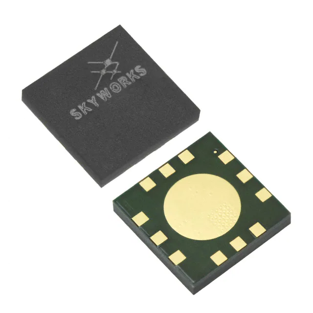
The SKY65116 is provided in a low-cost, Surface Mount
Technology (SMT) 8 x 8 mm Multi-Chip Module (MCM) package.
Figure 1 shows a functional block diagram for the SKY65116. The
pin configuration and package are shown in Figure 2. Signal pin
assignments and functional pin descriptions are provided in
Table 1.
Skyworks Solutions, Inc. • Phone [781] 376-3000 • Fax [781] 376-3100 • sales@skyworksinc.com • www.skyworksinc.com
200510I • Skyworks Proprietary and Confidential information • Products and Product Information are Subject to Change Without Notice • February 21, 2014
1
�12
11
VCC2
VCNT
VREF
DATA SHEET • SKY65116 LINEAR POWER AMPLIFIER
10
GND 1
9
GND
RFIN 2
8
RFOUT
GND 3
7
GND
6
GND
5
GND
VCC1
4
Y0694
Figure 2. SKY65116 Pinout– 12-Pin MCM Package
Table 1. SKY65116 Signal Descriptions
Pin
Name
Description
Ground
Pin
7
Name
GND
Description
1
GND
Ground
2
RFIN
RF input
8
RFOUT
RF output
3
GND
Ground
9
GND
Ground
4
VCC1
Stage 1 collector voltage
10
VCC2
Stage 2 collector voltage
5
GND
Ground
11
VCNT
PA on/off coltrol voltage
6
GND
Ground
12
VREF
Bias reference voltage
Technical Description
The SKY65116 is comprised of two amplifier stages. The
matching circuits for the input stage, inter-stage, and output
stage are contained within the device. The bias circuits for both
input and output stages are included within the device for
optimum temperature tracking performance.
The SKY65116 is internally matched for optimum linearity and
efficiency. The input and output stages are independently
supplied using the VCC1 and VCC2 supply lines, pins 4 and 10,
respectively. The bias reference voltage is supplied using a
common VREF (pin 12) line. The device can be switched on and
off using the VCNT signal (pin 11).
Skyworks Solutions, Inc. • Phone [781] 376-3000 • Fax [781] 376-3100 • sales@skyworksinc.com • www.skyworksinc.com
2
February 21, 2014 • Skyworks Proprietary and Confidential information • Products and Product Information are Subject to Change Without Notice • 200510I
�PRELIMINARY DATA SHEET • SKY65116 LINEAR POWER AMPLIFIER
Electrical and Mechanical Specifications
Typical performance characteristics over temperature of the
SKY65116 are illustrated in Figures 3 through 29.
The absolute maximum ratings of the SKY65116 are provided in
Table 2. The recommended operating conditions are specified in
Table 3 and electrical specifications are provided in Table 4.
Figure 34 shows the package dimensions for the 12-pin
SKY65116 MCM and Figure 35 provides the tape and reel
dimensions.
Table 2. SKY65116 Absolute Maximum Ratings (Note 1)
Parameter
Symbol
Min
Typical
Max
Units
+34.5
dBm
RF output power
POUT
Supply voltage
VCC1, VCC2, VREF, VCNT
Supply current
ICC
Power dissipation
PDISS
3.7
W
Case operating temperature
TC
–40
+85
°C
Storage temperature
TST
–55
+125
°C
Junction temperature
TJ
+150
°C
4.5
V
1300
mA
Note 1: Exposure to maximum rating conditions for extended periods may reduce device reliability. There is no damage to device with only one parameter set at the limit and all other
parameters set at or below their nominal values.
CAUTION: Although this device is designed to be as robust as possible, Electrostatic Discharge (ESD) can damage this device. This
device must be protected at all times from ESD. Static charges may easily produce potentials of several kilovolts on the
human body or equipment, which can discharge without detection. Industry-standard ESD precautions should be used at all
times.
Table 3. SKY65116 Recommended Operating Conditions
Parameter
Symbol
Min
Typical
Max
Units
3.6
4.0
V
4.0
V
Supply voltage
VCC
3.2
Reference voltage
VREF
3.2
3.6
Control voltage (power-up)
VCNT
2.7
3.6
Control voltage (power down)
VCNT
Operating frequency
f
390
Operating case temperature
TC
–40
0
+25
V
0.5
V
500
MHz
+85
°C
Skyworks Solutions, Inc. • Phone [781] 376-3000 • Fax [781] 376-3100 • sales@skyworksinc.com • www.skyworksinc.com
200510I • Skyworks Proprietary and Confidential information • Products and Product Information are Subject to Change Without Notice • February 21, 2014
3
�DATA SHEET • SKY65116 LINEAR POWER AMPLIFIER
Table 4. SKY65116 Electrical Characteristics
(VCC1 = VCC2 = VCNT = VREF = 3.6 V, TC = +25 °C, Z0 = 50 Ω, Unless Otherwise Specified)
Parameter
Symbol
Test Condition
Min
Typical
Max
Units
500
MHz
0.375
A
Frequency
F
Quiescent current
ICQ
No RF
390
0.1
0.33
Small signal gain
G
PIN = -15 dBm
33.5
35
dB
Input return loss
lS11l
PIN = -15 dBm
10
22
dB
Output return loss
lS22l
PIN = -15 dBm
4.5
6
dB
Output power
POUT
@ P1 dB
31.5
32.5
dBm
Power added efficiency
PAE
POUT @ P1 dB
35
42
%
Output IP3
OIP3
POUT = 25 dBm/tone
38
43
dBm
Noise figure
NF
PIN = -15 dBm
Thermal resistance
JC
Junction to case
6
7.5
17.6
Skyworks Solutions, Inc. • Phone [781] 376-3000 • Fax [781] 376-3100 • sales@skyworksinc.com • www.skyworksinc.com
4
February 21, 2014 • Skyworks Proprietary and Confidential information • Products and Product Information are Subject to Change Without Notice • 200510I
dB
˚C/W
�PRELIMINARY DATA SHEET • SKY65116 LINEAR POWER AMPLIFIER
Typical Performance Characteristics
(VCC1 = VCC2 = VCNT = VREF = 3.6 V, TC = +25 °C, Z0 = 50 Ω, Unless Otherwise Specified)
-40 °C
25 °C
85 °C
-40 °C
46
37
25 °C
85 °C
36
44
OIP3 (dBm)
Gain (dB)
35
34
33
42
Y0696
40
Y0695
32
38
31
15
390 400 410 420 430 440 450 460 470 480 490 500
17
19
21
Frequency (MHz)
3.6 V
4.0 V
3.2 V
46
35.5
35.0
44
34.5
42
OIP3 (dBm)
Gain (dB)
25
27
29
31
33
35
Figure 4. OIP3 vs Output Power /Tone Across Temperature
Figure 3. Gain vs Frequency Across Temperature
3.2 V
23
POUT/Tone (dBm)
34.0
3.6 V
4.0 V
40
33.5
Y0697
Y0698
38
33.0
36
32.5
20
390 400 410 420 430 440 450 460 470 480 490 500
22
24
Frequency (MHz)
3.2 V
28
30
32
Figure 6. OIP3 vs Output Power /Tone Across Voltage
Figure 5. Gain vs Frequency Across Voltage
0.36
26
POUT/Tone (dBm)
3.6 V
390 MHz
4.0 V
450 MHz
500 MHz
50
0.35
46
OIP3 (dBm)
0.34
0.32
42
0.31
38
0.30
0.29
Y0700
Y6099
ICQ (A)
0.33
34
-40
-15
+10
+35
+60
Temperature (°C)
Figure 7. ICQ vs Temperature Across Voltage
+85
15
17
19
21
23
25
27
29
POUT/Tone (dBm)
Figure 8. OIP3 vs Output Power/Tone Across Frequency
Skyworks Solutions, Inc. • Phone [781] 376-3000 • Fax [781] 376-3100 • sales@skyworksinc.com • www.skyworksinc.com
200510I • Skyworks Proprietary and Confidential information • Products and Product Information are Subject to Change Without Notice • February 21, 2014
5
�DATA SHEET • SKY65116 LINEAR POWER AMPLIFIER
25 °C
3.2 V
85 °C
-12
-15
-15
S11 (dB)
S11 (dB)
-40 °C
-12
-18
3.6 V
4.0 V
-18
-21
Y0701
Y0702
-21
-24
-24
390 400 410 420 430 440 450 460 470 480 490 500
390 400 410 420 430 440 450 460 470 480 490 500
Frequency (MHz)
Frequency (MHz)
Figure 10. S11 vs Frequency Across VCC
Figure 9. S11 vs Frequency Across Temperature
-40 °C
25 °C
3.2 V
85 °C
4.0 V
-5.5
S22 (dB)
-5.5
S22 (dB)
3.6 V
-5.0
-5.0
-6.0
-6.0
-6.5
Y0703
Y0704
-6.5
-7.0
-7.0
390 400 410 420 430 440 450 460 470 480 490 500
390 400 410 420 430 440 450 460 470 480 490 500
Frequency (MHz)
Frequency (MHz)
Figure 12. S22 vs Frequency Across VCC
Figure 11. S22 vs Frequency Across Temperature
-40 °C
25 °C
3.2 V
85 °C
3.6 V
4.0 V
7.0
7.5
6.8
6.5
6.0
Y0705
5.5
5.0
6.6
6.4
6.2
6.0
Y0706
Noise Figure (dB)
Noise Figure (dB)
7.0
5.8
390 400 410 420 430 440 450 460 470 480 490 500
390 400 410 420 430 440 450 460 470 480 490 500
Frequency (MHz)
Frequency (MHz)
Figure 13. Noise Figure vs Frequency Across Temperature
Figure 14. Noise Figure vs Frequency Across VCC
Skyworks Solutions, Inc. • Phone [781] 376-3000 • Fax [781] 376-3100 • sales@skyworksinc.com • www.skyworksinc.com
6
February 21, 2014 • Skyworks Proprietary and Confidential information • Products and Product Information are Subject to Change Without Notice • 200510I
�PRELIMINARY DATA SHEET • SKY65116 LINEAR POWER AMPLIFIER
-40 °C
25 °C
85 °C
-40 °C
25 °C
85 °C
1.8
50
1.6
42
34
ICC (A)
PAE (%)
1.4
1.2
1.0
26
Y0707
10
+23
+25
+27
+29
+31
+33
Y0708
0.8
18
0.6
0.4
+23
+35
+25
+31
+33
+35
Figure 16. ICC vs Output Power Across Temperature
Figure 15. PAE vs Output Power Across Temperature
3.6 V
3.2 V
4.0 V
52
1.6
46
1.4
40
3.6 V
4.0 V
1.2
ICC (A)
PAE (%)
+29
Output Power (dBm)
Output Power (dBm)
3.2 V
+27
34
1.0
28
0.8
22
0.4
10
+23
+25
+27
+29
+31
+33
Y0710
0.6
Y0709
16
+23
+35
+25
+31
+33
+35
Figure 18. ICC vs Output Power Across VCC
Figure 17. PAE vs Output Power Across VCC
450 MHz
+29
Output Power (dBm)
Output Power (dBm)
390 MHz
+27
390 MHz
500 MHz
450 MHz
500 MHz
1.8
48
1.6
40
ICC (A)
32
1.2
1.0
24
8
+22
+24
+26
+28
+30
+32
+34
Output Power (dBm)
Figure 19. PAE vs Output Power Across Frequency
+36
Y0712
0.8
16
Y0711
PAE (%)
1.4
0.6
0.4
+21
+23
+25
+27
+29
+31
+33
+35
Output Power (dBm)
Figure 20. ICC vs Output Power Across Frequency
Skyworks Solutions, Inc. • Phone [781] 376-3000 • Fax [781] 376-3100 • sales@skyworksinc.com • www.skyworksinc.com
200510I • Skyworks Proprietary and Confidential information • Products and Product Information are Subject to Change Without Notice • February 21, 2014
7
�DATA SHEET • SKY65116 LINEAR POWER AMPLIFIER
-40 °C
25 °C
85 °C
3.2 V
38
36
37
35
4.0 V
34
Gain (dB)
Gain (dB)
36
3.6 V
35
34
33
32
33
31
+21
Y0714
31
Y0713
32
30
+23
+25
+27
+29
+31
+33
+23 +24 +25 +26 +27 +28 +29 +30 +31 +32 +33 +34 +35
+35
Output Power (dBm)
Output Power (dBm)
Figure 21. Gain vs Output Power Across Temperature
390 MHz
450 MHz
Figure 22. Gain vs Output Power Across VCC
500 MHz
36
S11
+40
S21
S22
+30
35
+20
+10
SIJ Mag (dB)
33
32
0
-10
-20
-30
-40
Y0715
31
-50
30
+21
+23
+25
+27
+29
+31
+33
Y0716
Gain (dB)
34
-60
+35
300
350
Output Power (dBm)
36
400 MHz
550 MHz
450
500
550
600
550
600
Frequency (MHz)
Figure 23. Gain vs Output Power Across Frequency
350 MHz
500 MHz
400
Figure 24. S-Parameters vs Frequency
450 MHz
+34
+33
35
+32
P1 dB (dBm)
34
Gain (dB)
33
32
31
30
+31
+30
+29
+28
Y0718
29
+27
Y0717
28
27
26
0
+5
+10
+15
+20
+25
+30
+35
+26
300
350
400
450
500
Frequency (MHz)
Power Out (dBm)
Figure 25. Gain vs CW Power Out
Figure 26. P1dB vs Frequency
Skyworks Solutions, Inc. • Phone [781] 376-3000 • Fax [781] 376-3100 • sales@skyworksinc.com • www.skyworksinc.com
8
February 21, 2014 • Skyworks Proprietary and Confidential information • Products and Product Information are Subject to Change Without Notice • 200510I
�PRELIMINARY DATA SHEET • SKY65116 LINEAR POWER AMPLIFIER
350 MHz
500 MHz
+48
400 MHz
550 MHz
45
450 MHz
40
+46
35
PAE (%)
+44
+40
30
25
+38
+36
20
Y0720
OIP3 (dBm)
+42
Y0719
+34
+32
15
300
350
400
450
500
550
600
+30
15
16
17
18
19
20
21
Frequency (MHz)
22
Power Out/Tone (dBm)
Figure 27. OIP3 vs Output Power/Tone Across Frequency
(Tone Spacing = 1 MHz)
Figure 28. PAE at P1dB vs Frequency
DC/RF Response Time
(VCC1, VCC2, VREF = 3.6 V, VCNT = 0/3.6 V, TA = 25 °C unless otherwise specified)
DC Pulse (VCNT)
RF Pulse
Y0721
Figure 29. SKY65116 Rise/Fall Times
Table 5. SKY65116 Rise/Fall Times (Note 1)
Percent
Label
Rise/Fall
Time
RF-RF
Pulse
10-90
P3
Rise
1.13 μs
DC-RF
50-90
P4
Rise
13.45 μs
RF-RF
90-10
P5
Fall
0.034 μs
DC-RF
50-10
P6
Fall
3.66 μs
Note 1: 10 μF capacitor, C2 and 0.01 μF capacitor, C5 removed for rise-fall time measurements. Their purpose is to filter DC noise < 200 MHz due to long bias leads to power supply. No
noise observed with the removal of C2 and C5.
Skyworks Solutions, Inc. • Phone [781] 376-3000 • Fax [781] 376-3100 • sales@skyworksinc.com • www.skyworksinc.com
200510I • Skyworks Proprietary and Confidential information • Products and Product Information are Subject to Change Without Notice • February 21, 2014
9
�DATA SHEET • SKY65116 LINEAR POWER AMPLIFIER
Theory of Operation
The SKY65116 is comprised of two amplifier stages, and is
internally matched for optimum linearity and efficiency. The
matching circuits for the input stage, inter-stage, and output
stage are contained within the device. An on-chip active bias
circuit is included within the device for both input and output
stages providing for excellent gain tracking over temperature and
voltage variations. The module operates with all positive DC
voltages while maintaining high efficiency and good linearity. The
nominal operating voltage is 3.6 V for maximum power, but can
be operated at slightly lower voltages for other mobile
applications.
The input and output stages are independently supplied using the
VCC1 and VCC2 supply lines, pins 4 and 10, respectively. The bias
reference voltage is supplied using a common VREF (pin 12) line.
The module includes a silicon CMOS controller circuit to provide
an amplifier On/Off operation. VCNT (pin 11) is the PA on/off
control voltage to the CMOS controller for stages 1 and 2. 0 V =
Off, 3.6 V = On. Nominal “On” operating range is between 2.7 to
3.6 VDC. VCNT set to 0 VDC will force the amplifier into off mode,
drawing only microamperes of current.
Application Circuit Notes
Center Ground. It is extremely important that the device paddle
be sufficiently grounded for both thermal and stability reasons.
Multiple small vias are acceptable and will work well under the
device if solder migration is an issue.
Ground (Pins 1, 3, 5, 6, 7, 9). Attach all ground pins to the RF
ground plane with the largest diameter and lowest inductance via
that the layout will allow. Multiple small vias are also acceptable
and will work well under the device if solder migration is an issue.
RF_IN (Pin 2). Amplifier RF Input Pin. ZO = 50 W. The module
includes an onboard internal DC blocking capacitor. All impedance matching is provided internal to the module.
VCC1 (Pin 4). Supply voltage for the first stage collector bias
(typically 3.6 V). Bypassing of VCC1 is accomplished with C7 and
C8 and should be placed in the approximate location shown on
the evaluation board, but placement is not critical.
RF_OUT(Pin 8). Amplifier RF Output Pin. ZO = 50 W. The module
includes an onboard internal DC blocking capacitor. All
impedance matching is provided internal to the module.
VCC2 (Pin 10). Supply voltage for the output (final) stage collector
bias (typically 3.6 V). Bypassing of VCC2 is accomplished with C1
and C4 and should be placed in the approximate location shown
on the evaluation board, but placement is not critical.
VCNT(Pin 11). VCNT is the PA on/off control voltage to the silicon
CMOS controller for stages 1 and 2. 0 V = Off, 3.6 V = On.
Nominal “On” operating range is between 2.7 to 3.6 VDC. VCNT set
to 0 VDC will force the amplifier into standby mode.
VREF (Pin 12). Bias reference voltage for amplifier stages 1 and 2.
VREF should be operated over the same voltage range as VCC, with
a nominal voltage of 3.6 V.
Package and Handling Information
Since the device package is sensitive to moisture absorption, it is
baked and vacuum packed before shipping Instructions on the
shipping container label regarding exposure to moisture after the
container seal is broken must be followed. Otherwise, problems
related to moisture absorption may occur when the part is
subjected to high temperature during solder assembly.
The SKY65116 is rated to Moisture Sensitivity Level 3 (MSL3) at
260 °C. It can be used for lead or lead-free soldering. For
additional information, refer to the Skyworks Application Note,
Solder Reflow Information, document number 200164.
Care must be taken when attaching this product, whether it is
done manually or in a production solder reflow environment.
Production quantities of this product are shipped in a standard
tape and reel format.
Skyworks Solutions, Inc. • Phone [781] 376-3000 • Fax [781] 376-3100 • sales@skyworksinc.com • www.skyworksinc.com
10
February 21, 2014 • Skyworks Proprietary and Confidential information • Products and Product Information are Subject to Change Without Notice • 200510I
�PRELIMINARY DATA SHEET • SKY65116 LINEAR POWER AMPLIFIER
Evaluation Board Description
Evaluation Board Test Procedure
Skyworks SKY65116 Evaluation Board is used to test the
performance of the SKY65116 PA. The Evaluation Board
schematic diagram is shown in Figure 30. The schematic shows
the basic design of the board for the 390 to 500 MHz range. An
assembly drawing for the Evaluation Board is shown in Figure 31
and the layer detail is provided in Figures 32 and 33.
Use the following procedure to set up the SKY65116 Evaluation
Board for testing:
Circuit Design Considerations
The following design considerations are general in nature and
must be followed regardless of final use or configuration.
1. Paths to ground should be made as short as possible.
2. The ground pad of the SKY65116 PA has special electrical and
thermal grounding requirements. This pad is the main thermal
conduit for heat dissipation. Since the circuit board acts as the
heat sink, it must shunt as much heat as possible from the
amplifier. As such, design the connection to the ground pad to
dissipate the maximum wattage produced to the circuit board.
Multiple vias to the grounding layer are required.
3. Two external output bypass capacitors (0.01 F and 10 F)
are required on the VCC1 (pin 4) supply input. The same two
capacitors are also required on the VCC2 (pin 10) supply input
and on the VREF input (pin 12). Each of these capacitors
should be placed in parallel between the supply line and
ground. See Figure 30 for a detailed diagram.
1. Connect a +3.6 V supply to VCC1 and VCC2, and +3.6 V
supply to VREF and VCNT. If available, enable the current
limiting function of the VCC power supply to 1.5 A.
2. Connect a signal generator to the RF signal input port. Set it to
the desired RF frequency at a power level of 2 dBm or less to
the Evaluation Board but do NOT enable the RF signal.
3. Connect a spectrum analyzer to the RF signal output port.
4. Enable the power supply.
5. Enable the RF signal.
6. Take measurements.
NOTE: It is important that the VCC1 and VCC2 voltage source be
adjusted such that 3.6 V is measured at the board. The
high collector currents will drop the collector voltage
significantly if long leads are used. Adjust the bias
voltage to compensate.
4. VCC1 (pin 4) and VCC2 (pin 10) may be connected together at
the supply.
NOTE: Junction temperature (TJ) of the device increases with a
poor connection to the ground pad and ground. This
reduces the life of the device.
Skyworks Solutions, Inc. • Phone [781] 376-3000 • Fax [781] 376-3100 • sales@skyworksinc.com • www.skyworksinc.com
200510I • Skyworks Proprietary and Confidential information • Products and Product Information are Subject to Change Without Notice • February 21, 2014
11
�DATA SHEET • SKY65116 LINEAR POWER AMPLIFIER
Reference
Voltage
C3
10 μF
C5
0.01 μF
C6
0.01 μF
C2
10 μF
PA Control
Voltage
VCC
12
VCNT
VREF
1
10
C1
10 μF
VCC2
11
C4
0.01 μF
GND
GND
RFIN
RFOUT
9
RF out
RF in
2
8
50 Ω transmission
line
50 Ω transmission
line
GND
GND
4
7
GND
GND
VCC1
3
5
6
VCC
C7
10 μF
C8
0.01 μF
S747
VCC2
VCNT
VREF
VCC1
GND
GND
GND
GND
Figure 30. SKY65116 Evaluation Board Schematic
J1
C2
C3
C1
C5
C6
RFIN
C4
J2
J3
RFOUT
C8
C7
S751
Figure 31. Evaluation Board Assembly Diagram
Skyworks Solutions, Inc. • Phone [781] 376-3000 • Fax [781] 376-3100 • sales@skyworksinc.com • www.skyworksinc.com
12
February 21, 2014 • Skyworks Proprietary and Confidential information • Products and Product Information are Subject to Change Without Notice • 200510I
�PRELIMINARY DATA SHEET • SKY65116 LINEAR POWER AMPLIFIER
Layer 1: Top -- Metal
Layer 2: Ground
Layer 3: Ground
Layer 4: Solid Ground Plane
S752
Figure 32. Evaluation Board Layer Detail
Skyworks Solutions, Inc. • Phone [781] 376-3000 • Fax [781] 376-3100 • sales@skyworksinc.com • www.skyworksinc.com
200510I • Skyworks Proprietary and Confidential information • Products and Product Information are Subject to Change Without Notice • February 21, 2014
13
�DATA SHEET • SKY65116 LINEAR POWER AMPLIFIER
Cross Section
Name Thickness (mils) Material
εr
L1
1.4
–
Lam1
12
L2_GND
1.4
Cu, 1 oz.
–
4
FR4-4
4.35
L3_GND
1.4
Cu, 1 oz.
–
Lam3
12
FR4-12
4.35
L4
1.4
Cu, 1 oz.
–
Lam2
Cu
Rogers 4003-12 3.38
Y0723
8.385
6x 4.093
Figure 33. Evaluation Board Layer Detail – Physical Characteristics
B
Pin 1
Indicator
C
(3.4)
( 0.3)
Solder Mask Opening
( 0.15)
Metal Pad
Pin 1 Indicator
12x SMT Pad
Top
Pin 1
(2.7)
0
8.385
A
4x 1.91
1.45 ± 0.1
0.15 A B C
A
0
0.1
12x SMT Pad
4x 1.65
6x 4.093
5.080
Solder Mask Opening
0.15 A B C
0.15 A B C
0.793 ± 0.1
(0.1)
Metal Pad Edge
Detail A
Pad
3x - This rotationo
3x - Rotated 180
3x - Rotated 90o
3x - Rotated 90o
0.81 ± 0.05
Notes:
Y0724
1. Dimensions and tolerances in accordance with ASME Y14.5M–1994.
2. All measurements are in millimeters.
3. Pad definitions per details on drawing.
Figure 34. SKY65116 12-Pin MCM Package Dimensions
Skyworks Solutions, Inc. • Phone [781] 376-3000 • Fax [781] 376-3100 • sales@skyworksinc.com • www.skyworksinc.com
14
February 21, 2014 • Skyworks Proprietary and Confidential information • Products and Product Information are Subject to Change Without Notice • 200510I
�PRELIMINARY DATA SHEET • SKY65116 LINEAR POWER AMPLIFIER
12.00 ± 1.10
2.00 ± 0.10
4.00 ± 0.10
Pin 1
Ø1.50 ± 0.10
1.75 ± 0.10
B
A
A
5° Max
16.00 + 0.30
–0.10
7.50 ± 0.10
8.88 ± 0.10 (Bo)
0.318 ± 0.013T
B
Ø1.50 + 0.25
2.14 ± 0.10 (Ko)
8° Max
Section B
8.89 ± 0.10 (Ao)
Section A
Notes:
1. Carrier tape material: black conductive polycarbonate or polystyrene.
2. Cover tape: transparent conductive pressure sensitive adhesive (PSA) material, 13.3 mm width.
3. ESD-surface resistivity shall be < / =1 X 10⁸ ohms/square per EIA, JEDEC TNR specification.
4. All dimensions are in millimeters
Y0725
Figure 35. SKY65116 12-Pin MCM Tape and Reel Dimensions
Skyworks Solutions, Inc. • Phone [781] 376-3000 • Fax [781] 376-3100 • sales@skyworksinc.com • www.skyworksinc.com
200510I • Skyworks Proprietary and Confidential information • Products and Product Information are Subject to Change Without Notice • February 21, 2014
15
�DATA SHEET • SKY65116 LINEAR POWER AMPLIFIER
Ordering Information
Model Name
SKY65116 390-500 MHz Linear Power Amplifier
Manufacturing Part Number
SKY65116-21
Evaluation Kit Part Number
TW14-D621
Copyright © 2006, 2008-2009, 2014 Skyworks Solutions, Inc. All Rights Reserved.
Information in this document is provided in connection with Skyworks Solutions, Inc. (“Skyworks”) products or services. These materials, including the information contained herein, are provided by
Skyworks as a service to its customers and may be used for informational purposes only by the customer. Skyworks assumes no responsibility for errors or omissions in these materials or the
information contained herein. Skyworks may change its documentation, products, services, specifications or product descriptions at any time, without notice. Skyworks makes no commitment to
update the materials or information and shall have no responsibility whatsoever for conflicts, incompatibilities, or other difficulties arising from any future changes.
No license, whether express, implied, by estoppel or otherwise, is granted to any intellectual property rights by this document. Skyworks assumes no liability for any materials, products or
information provided hereunder, including the sale, distribution, reproduction or use of Skyworks products, information or materials, except as may be provided in Skyworks Terms and Conditions
of Sale.
THE MATERIALS, PRODUCTS AND INFORMATION ARE PROVIDED “AS IS” WITHOUT WARRANTY OF ANY KIND, WHETHER EXPRESS, IMPLIED, STATUTORY, OR OTHERWISE, INCLUDING FITNESS FOR A
PARTICULAR PURPOSE OR USE, MERCHANTABILITY, PERFORMANCE, QUALITY OR NON-INFRINGEMENT OF ANY INTELLECTUAL PROPERTY RIGHT; ALL SUCH WARRANTIES ARE HEREBY EXPRESSLY
DISCLAIMED. SKYWORKS DOES NOT WARRANT THE ACCURACY OR COMPLETENESS OF THE INFORMATION, TEXT, GRAPHICS OR OTHER ITEMS CONTAINED WITHIN THESE MATERIALS. SKYWORKS
SHALL NOT BE LIABLE FOR ANY DAMAGES, INCLUDING BUT NOT LIMITED TO ANY SPECIAL, INDIRECT, INCIDENTAL, STATUTORY, OR CONSEQUENTIAL DAMAGES, INCLUDING WITHOUT LIMITATION,
LOST REVENUES OR LOST PROFITS THAT MAY RESULT FROM THE USE OF THE MATERIALS OR INFORMATION, WHETHER OR NOT THE RECIPIENT OF MATERIALS HAS BEEN ADVISED OF THE
POSSIBILITY OF SUCH DAMAGE.
Skyworks products are not intended for use in medical, lifesaving or life-sustaining applications, or other equipment in which the failure of the Skyworks products could lead to personal injury,
death, physical or environmental damage. Skyworks customers using or selling Skyworks products for use in such applications do so at their own risk and agree to fully indemnify Skyworks for any
damages resulting from such improper use or sale.
Customers are responsible for their products and applications using Skyworks products, which may deviate from published specifications as a result of design defects, errors, or operation of
products outside of published parameters or design specifications. Customers should include design and operating safeguards to minimize these and other risks. Skyworks assumes no liability for
applications assistance, customer product design, or damage to any equipment resulting from the use of Skyworks products outside of stated published specifications or parameters.
Skyworks, the Skyworks symbol, and “Breakthrough Simplicity” are trademarks or registered trademarks of Skyworks Solutions, Inc., in the United States and other countries. Third-party brands
and names are for identification purposes only, and are the property of their respective owners. Additional information, including relevant terms and conditions, posted at www.skyworksinc.com,
are incorporated by reference.
Skyworks Solutions, Inc. • Phone [781] 376-3000 • Fax [781] 376-3100 • sales@skyworksinc.com • www.skyworksinc.com
16
February 21, 2014 • Skyworks Proprietary and Confidential information • Products and Product Information are Subject to Change Without Notice • 200510I
�


 工商网监
湘ICP备2023018690号
工商网监
湘ICP备2023018690号