DATA SHEET
SKY65135: WLAN Power Amplifier
Applications
• IEEE802.11 b/g WLAN • ISM band • WCS fixed wireless • Wireless access nodes
Description
Skyworks SKY65135 is a Microwave Monolithic Integrated Circuit (MMIC) Power Amplifier (PA) with superior output power, linearity, and efficiency. These features make the SKY65135 ideal for Wireless Local Area Network (WLAN) applications. The device is fabricated using Skyworks high reliability Indium Gallium Phosphide (InGaP) Heterojunction Bipolar Transistor (HBT) technology. The device is internally matched and mounted in a 20-pin, 6 x 6 mm Multi-Chip Module (MCM) Surface-Mounted Technology (SMT) package, which allows for a highly manufacturable low cost solution. The device package and pinout for the 20-pin MCM are shown in Figure 1. A block diagram of the SKY65135 is shown in Figure 2.
Features
• Linear output power of +31 dBm for IEEE802.11b mask • Linear output power of +30 dBm for IEEE802.11g mask • Three percent EVM at POUT >+27 dBm • High gain of 33 dB • Output power detector: 20 dB dynamic range • Superior gain flatness • Internal RF match and bias circuits • Small footprint, MCM (20-pin, 6 x 6 mm) Pb-free (MSL3, 250 °C per JEDEC J-STD-020) SMT package Skyworks offers lead (Pb)-free RoHS (Restriction of Hazardous Substances) compliant packaging.
RF_IN
18
GND
GND
GND GND GND VC_BIAS VREF1 VREF2
1
20
19
GND
17
16
VCC1 VCC_DET V_DET VCC2 VDET_CNTL VCC3
2
15
3
14
4
13
5
12
6
7
8
9
10
11
VREF3
GND
RF_OUT
GND
S414
Figure 1. SKY65135 Pinout – 20-Pin MCM (Top View)
Skyworks Solutions, Inc. • Phone [781] 376-3000 • Fax [781] 376-3100 • sales@skyworksinc.com • www.skyworksinc.com
200436D • Skyworks Proprietary and Confidential information • Products and Product Information are Subject to Change Without Notice • March 28, 2007 1
�DATA SHEET • SKY65135 WLAN PA
VCC1
VREF1, VREF2 VREF3
VC_BIAS
VCC3
VCC_DET
Active Bias
Detector
V_DET
RF_IN
Input Match Stage 1 PA
Inter-Stage Match
Stage 2 PA
VCC2
Inter-Stage Match
Output Match Stage 3 PA
RF_OUT
S413
Figure 2. SKY65135 Block Diagram
Technical Description
The SKY65135 PA contains all of the needed RF matching and DC biasing circuits. The device also provides an output power detector voltage. The SKY65135 is a three-stage, HBT InGaP device optimized for high linearity and power efficiency. These features make the device suitable for wideband digital applications, where PA linearity and power consumption are of critical importance (e.g., WLANs). The device has been characterized with the highest specified data rates for 802.11b (11 Mbps) and 802.11g (54 Mbps). Under these stringent test conditions, the device exhibits excellent spectral purity and power efficiency.
Care must be taken when attaching this product, whether it is done manually or in a production solder reflow environment. Production quantities of this product are shipped in a standard tape and reel format. For packaging details, refer to the Skyworks Application Note, Tape and Reel, document number 101568.
Electrical and Mechanical Specifications
Signal pin assignments and functional pin descriptions are described in Table 1. The absolute maximum ratings of the SKY65135 are provided in Table 2. Electrical specifications are provided in Table 3. Typical performance characteristics are shown in Figures 3 through 11. Figure 12 provides a typical evaluation board schematic. An assembly drawing for the Evaluation Board is shown in Figure 13 and the layer detail is provided in Figure 14. The layer detail physical characteristics are noted in Figure 15. The phone board layout footprint for the SKY65135 is shown in Figure 16. Package dimensions for the 20-pin MCM are shown in Figure 17, and tape and reel dimensions are provided in Figure 18.
Package and Handling Information
Since the device package is sensitive to moisture absorption, it is baked and vacuum packed before shipping. Instructions on the shipping container label regarding exposure to moisture after the container seal is broken must be followed. Otherwise, problems related to moisture absorption may occur when the part is subjected to high temperature during solder assembly. The SKY65135 is rated to Moisture Sensitivity Level 3 (MSL3) at 250 °C. It can be used for lead or lead-free soldering. For additional information, refer to Skyworks Application Note, PCB Design and SMT Assembly/Rework Guidelines for MCM-L Packages, document number 101752.
Electrostatic Discharge (ESD) Sensitivity
The SKY65135 is a static-sensitive electronic device. Do not operate or store near strong electrostatic fields. Take proper ESD precautions.
Skyworks Solutions, Inc. • Phone [781] 376-3000 • Fax [781] 376-3100 • sales@skyworksinc.com • www.skyworksinc.com
2 March 28, 2007 • Skyworks Proprietary and Confidential information • Products and Product Information are Subject to Change Without Notice • 200436D
�DATA SHEET • SKY65135 WLAN PA
Table 1. SKY65135 Signal Descriptions
Pin # 1 2 3 4 5 6 7 8 9 10 GND GND GND VC_BIAS VREF1 VREF2 VREF3 GND RF_OUT GND Name Ground Ground Ground Bias voltage Bias reference voltage 1 Bias referance voltage 2 Bias referance voltage 3 Ground RF output Ground Description Pin # 11 12 13 14 15 16 17 18 19 20 VCC3 VDET_CNTL VCC2 V_DET VCC_DET VCC1 GND RF_IN GND GND Name Description Stage 3 collector voltage Detector voltage control Stage 2 collector voltage Detector output signal Detector supply voltage Stage 1 collector voltage Ground RF input Ground Ground
Table 2. SKY65135 Absolute Maximum Ratings (Note 1)
Parameter RF output power Supply voltage, measured at pin of package (Note 2) 3rd stage supply voltage Total supply current (ICC + IBIAS + IREF) Power dissipation Case operating temperature Storage temperature Junction temperature TC TST TJ –40 –55 POUT VREF1, VREF2, VREF3, VCC1, VCC2, and VCC_DET VCC3, VC_BIAS ICC_TOTAL Symbol Minimum Maximum 30 4 Units dBm V
6 1200 4.0 +85 +125 +150
V mA W °C °C °C
Note 1: Exposure to maximum rating conditions for extended periods may reduce device reliability. There is no damage to device with only one parameter set at the limit and all other parameters set at or below their nominal value. Note 2: Evaluation Board supply voltage levels can be different. Refer to the Evaluation Board schematic diagram in Figure 12.
Table 3. SKY65135 Recommended Operating Conditions
Parameter RF input power Supply voltage, measured at pin of package (Note 1) PIN VREF1, VREF2, and VREF3 VCC1 and VCC2 VCC_DET VCC3 and VC_BIAS Case operating temperature Storage temperature TC TST 2.3 3.0 3.3 4.5 –40 –55 2.5 3.3 3.6 5.0 Symbol Minimum Typical Maximum –6 2.7 3.6 3.9 5.5 +85 +125 Units dBm V V V V °C °C
Note 1: Evaluation Board supply voltage levels can be different. Refer to the Evaluation Board schematic diagram in Figure 12.
Skyworks Solutions, Inc. • Phone [781] 376-3000 • Fax [781] 376-3100 • sales@skyworksinc.com • www.skyworksinc.com
200436D • Skyworks Proprietary and Confidential information • Products and Product Information are Subject to Change Without Notice • March 28, 2007 3
�DATA SHEET • SKY65135 WLAN PA
Table 4. SKY65135 Electrical Specifications (VCC1 = VCC2 = 3.3 V, VCC3 = 5 V, TC = +25 °C, Test Frequency = 2.442 GHz unless otherwise noted)
Parameter Symbol Test Condition Min Typical Max Units
Using IEEE802.11b Complimentary Code Keying Input Signal, Data Rate = 11 Mbps Total supply current Output power (Note 1) Power added efficiency (Note 2) Ramp-up/ramp-down (Note 3) ICC_TOTAL POUT PAE TS 1150 31 25
很抱歉,暂时无法提供与“SKY65135-21”相匹配的价格&库存,您可以联系我们找货
免费人工找货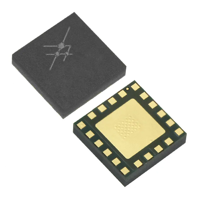


 工商网监
湘ICP备2023018690号
工商网监
湘ICP备2023018690号
