PRELIMINARY DATA SHEET
SKY66005-11: 850 to 920 MHz, +19 dBm Linear Power
Amplifier
Applications
Residential femtocells
VEN
WCDMA, Bands 5, 6, 18, 19, and 26
MMIC
VCC1
Small cells
Power Stage
Bias
Driver Stage
Bias
RF_IN
Features
Input
Match
DA
Inter-Stage
Match
PA
Output
Match
RF_OUT
VCC2
CPL_OUT
CPL_IN
Small signal gain: 29 dB
ACLR at POUT = +29 dBm: -51 dBc
S2993
PA on/off control
Figure 1. SKY66005-11 Linear PA Block Diagram
I/O impedance internally matched to 50 Ω
Single DC supply: 3.3 V to 4.6 V
Description
Minimal number of external components required
The SKY66005-11 linear power amplifier (PA) is a fully matched
surface mount module developed for WCDMA applications
operating from 850 to 920 MHz. The device meets the stringent
spectral linearity requirements of WCDMA femtocell applications
with high power-added efficiency. An integrated directional
coupler eliminates the need for any external coupler.
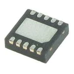
Small footprint MCM (10-pin, 3 x 3 mm) package
(MSL3, 260 C per JEDEC J-STD-020)
Skyworks GreenTM products are compliant with
all applicable legislation and are halogen-free.
For additional information, refer to Skyworks
Definition of GreenTM, document number
SQ04–0074.
VCC1
1
10
VCC2
RF_IN
2
9
RF_OUT
GND
3
8
CPL_IN
GND
4
7
GND
VEN
5
6
CPL_OUT
S2992
The GaAs MMIC contains all active amplifier circuitry, which
includes input and interstage matching circuits. An output match
into a 50 Ω load, realized off-chip within the module package,
optimizes efficiency and power performance.
The SKY66005-11 is manufactured with Skyworks InGaP GaAs
HBT process, which provides for all positive voltage DC supply
operation and maintains high efficiency and good linearity. The
primary bias to the device can be supplied directly from any
suitable power supply with an output of 4.2 V. Power down is
achieved by setting the VEN pin to 0 V. No external supply side
switch is needed since typical “off” leakage is a few microamps
with full primary voltage supplied from the main power supply.
The SKY66005-11 is packaged in a 10-pin, 3 x 3 mm Multi-Chip
Module (MCM), which allows for a highly manufacturable low-cost
solution.
A functional block diagram of the SKY66005-11 is shown in
Figure 1. The 10-pin MCM package and pinout are shown in
Figure 2. Signal pin assignments and functional pin descriptions
are provided in Table 1.
Figure 2. SKY66005-11 Pinout
(Top View)
Skyworks Solutions, Inc. • Phone [781] 376-3000 • Fax [781] 376-3100 • sales@skyworksinc.com • www.skyworksinc.com
202504D • Skyworks Proprietary Information • Products and Product Information are Subject to Change Without Notice • October 6, 2017
1
�PRELIMINARY DATA SHEET • SKY66005-11: 850 TO 920 MHz, +19 dBm LINEAR POWER AMPLIFIER
Table 1. SKY66005-11 Signal Descriptions
Pin
Name
Description
Pin
Input stage supply voltage
6
Name
Description
1
VCC1
CPL_OUT
RF coupler output
2
RF_IN
RF input port
3
GND
Ground
7
GND
Ground
8
CPL_IN
RF coupler input
4
GND
Ground
9
RF_OUT
RF output port
5
VEN
Enable
10
VCC2
Output stage supply voltage
Technical Description
Electrical and Mechanical Specifications
The SKY66005-11 PA contains all of the needed RF matching and
DC biasing circuits. The device is a two-stage, HBT InGaP device
optimized for high linearity and power efficiency. These features
make the device suitable for wideband digital applications where
PA linearity and power consumption are of critical importance
(e.g., small cell and infrastructure applications).
The absolute maximum ratings of the SKY66005-11 are provided
in Table 2. The recommended operating conditions are specified
in Table 3 and electrical specifications are provided in Table 4.
A typical performance plot of ACLR5 versus output power is
shown in Figure 3.
The device is designed for standard WCDMA modulated signals.
Under these stringent test conditions, the device exhibits excellent
spectral purity and power efficiency.
Table 2. SKY66005-11 Absolute Maximum Ratings1
Parameter
Supply voltage (VCC1, VCC2)
Symbol
VCC
Minimum
Maximum
Units
0
+4.6
V
Total supply current
ICC
700
mA
Logic control input voltage (VEN)
VCTL
-0.5
3.1
V
Case operating temperature2
TC
-40
+85
C
Storage temperature
TSTG
-55
Junction temperature
TJ
Thermal resistance
ΘJC
Electrostatic discharge:
ESD
Charged Device Model (CDM), Class 3
Human Body Model (HBM), Class 1C
Machine Model (MM), Class A
+150
C
+150
C
60
C/W
1000
1000
50
V
V
V
1 Exposure to maximum rating conditions for extended periods may reduce device reliability. There is no damage to device with only one parameter set at the limit and all other parameters
set at or below their nominal value. Exceeding any of the limits listed here may result in permanent damage to the device.
2 Case operating temperature (Tc) refers to the temperature of the bottom ground pad.
ESD HANDLING: Although this device is designed to be as robust as possible, electrostatic discharge (ESD) can damage this device.
This device must be protected at all times from ESD when handling or transporting. Static charges may easily produce
potentials of several kilovolts on the human body or equipment, which can discharge without detection.
Industry-standard ESD handling precautions should be used at all times.
Skyworks Solutions, Inc. • Phone [781] 376-3000 • Fax [781] 376-3100 • sales@skyworksinc.com • www.skyworksinc.com
2
October 6, 2017 • Skyworks Proprietary Information • Products and Product Information are Subject to Change Without Notice • 202504D
�PRELIMINARY DATA SHEET • SKY66005-11 850 TO 920 MHz, +19 dBm LINEAR POWER AMPLIFIER
Table 3. SKY66005-11 Recommended Operating Conditions
Parameter
Symbol
Min
Typ
Max
Units
897
MHz
Frequency range
f
869
Supply voltage (VCC1, VCC2) 1
VCC
4.0
4.2
4.6
V
Logic control input voltage:
Logic high
Logic low
VIH
VIL
1.35
0
1.80
3.10
0.5
V
V
PA enable current
IEN
很抱歉,暂时无法提供与“SKY66005-11”相匹配的价格&库存,您可以联系我们找货
免费人工找货- 国内价格
- 1+12.87360
- 200+4.98960
- 500+4.81680
- 1000+4.73040