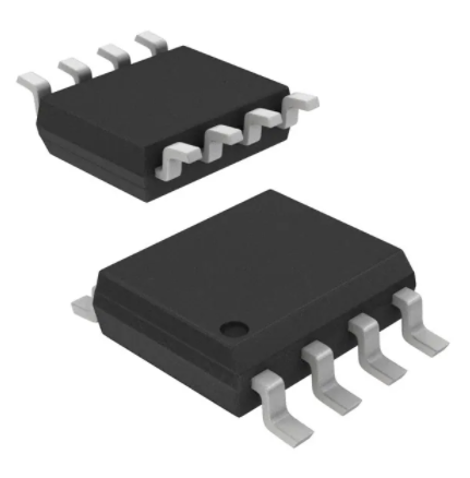
STP6621
P Channel Enhancement Mode MOSFET
-18.0A
SCRIPTION
STP6621 is the P-Channel logic enhancement mode power field effect transistor which
is produced using high cell density, DMOS trench technology. This high density
process is especially tailored to minimize on-state resistance. These devices are
particularly suited for low voltage application, noteook power management ane ther
battery powered circuits where high-side witching.
PIN CONFIGURATION
SOP-8
FEATURE
�
�
�
�
�
-60V/-10.0A, RDS(ON) = 23mΩ (Typ.)
@VGS =-10V
-60V/-8.0A, RDS(ON) = 28mΩ
@VGS = -4.5V
Super high density cell design for
extremely low RDS(ON)
Exceptional on-resistance and maximum
DC current capability
SOP-8 package design
PART MARKING
SOP-8
STANSON TECHNOLOGY
120 Bentley Square, Mountain View, Ca 94040 USA
www.stansontech.com
.
STP6621 2010. V1
�STP6621
P Channel Enhancement Mode MOSFET
-18.0A
ABSOULTE MAXIMUM RATINGS (Ta = 25℃ Unless otherwise noted )
Symbol
Typical
Unit
Drain-Source Voltage
VDSS
-60
V
Gate-Source Voltage
VGSS
±20
V
ID
-18.0
-11.0
A
IDM
-50
A
IS
-4.3
A
PD
3.1
2.0
W
TJ
-55/150
℃
Storgae Temperature Range
TSTG
-55/150
℃
Thermal Resistance-Junction to Ambient
RθJA
70
Parameter
Continuous Drain Current
(TJ=150℃)
TA=25℃
TA=70℃
Pulsed Drain Current
Continuous Source Current
(Diode Conduction)
Power Dissipation
TA=25℃
TA=70℃
Operation Junction Temperature
℃/W
STANSON TECHNOLOGY
120 Bentley Square, Mountain View, Ca 94040 USA
www.stansontech.com
.
STP6621 2010. V1
�STP6621
P Channel Enhancement Mode MOSFET
-18.0A
ELECTRICAL CHARACTERISTICS ( Ta = 25℃ Unless otherwise noted )
Parameter
Symbol
Condition
Min
Typ
Max Unit
V(BR)DSS
VGS=0V,ID=-250uA
-60
VGS(th)
VDS=VGS,ID=-250 uA
-0.8
Gate Leakage Current
IGSS
Zero Gate Voltage Drain
Current
IDSS
On-State Drain Current
ID(on)
VDS=-5V,VGS=10V
Drain-source On-Resistance
RDS(on)
VGS=-10V, ID=-10A
VGS=-4.5V, ID=-8A
Forward Tran Conductance
gfs
VDS=-5V,ID=-6.7A
18
Diode Forward Voltage
VSD
IS=-2.3A,VGS=0V
-0.7
-1.0
47
55
Static
Drain-Source Breakdown
Voltage
Gate Threshold Voltage
V
-2.5
V
VDS=0V,VGS=±20V
±100
nA
VDS=-48V,VGS=0V
VDS=-48V,VGS=0V
TJ=85℃
-1
-10
-18
uA
A
0.023 0.030
0.028 0.038
Ω
S
V
Dynamic
Total Gate Charge
Qg
VDS=-30V,VGS=-10
ID≡-6.2A
Gate-Source Charge
Qgs
Gate-Drain Charge
Qgd
9.3
Input Capacitance
Ciss
2410
Output Capacitance
Coss
Reverse TransferCapacitance
Crss
125
Turn-On Time
td(on)
9.8
Turn-Off Time
tr
td(off)
VDS =-30V,VGS=0V
f=1MHz
VDS=-30V,RL=4.7Ω
VGS=-10V,RGEN=3Ω
tf
9.2
179
6.1
nC
pF
nS
44
12.9
STANSON TECHNOLOGY
120 Bentley Square, Mountain View, Ca 94040 USA
www.stansontech.com
.
STP6621 2010. V1
�STP6621
P Channel Enhancement Mode MOSFET
-18.0A
TYPICAL CHARACTERICTICS
STANSON TECHNOLOGY
120 Bentley Square, Mountain View, Ca 94040 USA
www.stansontech.com
.
STP6621 2010. V1
�STP6621
P Channel Enhancement Mode MOSFET
-18.0A
TYPICAL CHARACTERICTICS
STANSON TECHNOLOGY
120 Bentley Square, Mountain View, Ca 94040 USA
www.stansontech.com
.
STP6621 2010. V1
�STP6621
P Channel Enhancement Mode MOSFET
-18.0A
SOP-8 PACKAGE OUTLINE
STANSON TECHNOLOGY
120 Bentley Square, Mountain View, Ca 94040 USA
www.stansontech.com
.
STP6621 2010. V1
�
很抱歉,暂时无法提供与“STP6621”相匹配的价格&库存,您可以联系我们找货
免费人工找货