®
2SD2012
NPN SILICON POWER TRANSISTOR
s s s
HIGH DC CURRENT GAIN LOW SATURATION VOLTAGE INSULATED PACKAGE FOR EASY MOUNTING
APPLICATIONS GENERAL PURPOSE POWER AMPLIFIERS s GENERAL PURPOSE SWITCHING
s
DESCRIPTION The 2SD2012 is a silicon NPN power transistor housed in TO-220F insulated package. It is inteded for power linear and switching applications.
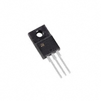
3 1 2
TO-220F
INTERNAL SCHEMATIC DIAGRAM
ABSOLUTE MAXIMUM RATINGS
Symbol V CBO V CEO V EBO IC I CM IB P tot Visol T stg Tj Parameter Collector-Base Voltage (I E = 0 ) Collector-Emitter Voltage (I B = 0 ) Emitter-Base Voltage (I C = 0 ) Collector Current Collector Peak Current (t p < 5 m s) Base Current Total Dissipation at T c ≤ 2 5 o C Insulation Withstand Voltage (RMS) from All Three Leads to Exernal Heatsink Storage Temperature Max. Operating Junction Temperature Value 60 60 7 3 6 0.5 25 1500 -65 to 150 150 Unit V V V A A A W V
o o
C C
October 2003
1/5
�2SD2012
THERMAL DATA
R thj-case Thermal Resistance Junction-case Max 5
o
C/W
ELECTRICAL CHARACTERISTICS (Tcase = 25 oC unless otherwise specified)
Symbol I CBO I EBO Parameter Collector Cut-off Current (I E = 0 ) Emitter Cut-off Current (I C = 0 ) Test Conditions V CB = 6 0 V V EB = 7 V I C = 5 0 mA 60 Min. Typ. Max. 100 100 Unit µA µA V
V (BR)CEO ∗ Collector-Emitter Breakdown Voltage (I B = 0) V CE(sat) ∗ V BE ∗ h FE ∗ fT C CBO Collector-Emitter Saturation Voltage Base-Emitter Voltage DC Current Gain Transition frequency Collector-Base Capacitance
IC = 2 A I C = 0 .5 A I C = 0 .5 A IC = 2 A V CE = 5 V V CB = 1 0 V IE = 0
I B = 0 .2 A V CE = 5 V V CE = 5 V V CE = 5 V I C = 0 .5 A f = 1 M Hz 100 20
0.4 0.75
1 1 320
V V
3 35
MHz pF
∗ Pulsed: Pulse duration = 300 µs, duty cycle ≤ 2 %
Safe Operating Area
Derating Curve
2/5
�2SD2012
DC Current Gain Collector Emitter Saturation Voltage
Base Emitter On Voltage
3/5
�2SD2012
TO-220F MECHANICAL DATA
DIM. MIN. A B D E F F1 G G1 H L2 L4 L6 L7 L8 Dia 3.08 9.45 15.67 8.99 3.30 3.28 0.121 2.34 9.96 15.80 10.05 16.07 9.39 0.372 0.617 0.354 0.130 0.129 5.08 2.54 2.74 10.36 0.092 0.392 0.622 0.396 0.633 0.370 4.50 2.34 2.56 0.45 0.70 0.50 mm TYP. MAX. 4.90 2.74 2.96 0.60 0.90 1.47 0.200 0.100 0.108 0.408 MIN. 0.177 0.092 0.101 0.018 0.028 0.020 inch TYP. MAX. 0.193 0.108 0.117 0.024 0.035 0.058
4/5
�2SD2012
Information furnished is believed to be accurate and reliable. However, STMicroelectronics assumes no responsibility for the consequences of use of such information nor for any infringement of patents or other rights of third parties which may result from its use. No license is granted by implication or otherwise under any patent or patent rights of STMicroelectronics. Specification mentioned in this publication are subject to change without notice. This publication supersedes and replaces all information previously supplied. STMicroelectronics products are not authorized for use as critical components in life support devices or systems without express written approval of STMicroelectronics. The ST logo is a trademark of STMicroelectronics. All other names are the property of their respective owners. © 2003 STMicroelectronics – All Rights reserved STMicroelectronics GROUP OF COMPANIES Australia - Belgium - Brazil - Canada - China - Czech Republic - Finland - France - Germany - Hong Kong - India - Israel - Italy - Japan Malaysia - Malta - Morocco - Singapore - Spain - Sweden - Switzerland - United Kingdom - United States. http://www.st.com
5/5
�
很抱歉,暂时无法提供与“2SD2012”相匹配的价格&库存,您可以联系我们找货
免费人工找货