1. 物料型号:74AC74,这是一个由SGS-THOMSON MICROELECTRONICS生产的高速CMOS D型触发器。
2. 器件简介:
- 74AC74是一款高速CMOS八路D型触发器,具有预置和清除功能,采用亚微米硅门和双层金属布线C²MOS技术制造。
- 它具有300MHz(典型值)的高速度和低功耗(最大4µA)特性,以及高噪声免疫能力和对称的输出阻抗。
3. 引脚分配:
- 1,13:1CLR, 2CLR(异步复位 - 直接输入)
- 2,12:1D,2D(数据输入)
- 3,11:1CK, 2CK(时钟输入,低至高边缘触发)
- 4,10:1PR,2PR(异步置位 - 直接输入)
- 5,9:1Q,2Q(真触发器输出)
- 6,8:1Q,2Q(互补触发器输出)
- 7:GND(地)
- 14:Vcc(正电源电压)
4. 参数特性:
- 工作电压范围:2V至6V
- 最大时钟频率:300MHz(典型值)
- 低功耗:4µA(最大值)
- 高噪声免疫:Vcc的28%
- 对称的输出阻抗:24mA(最小值)
5. 功能详解:
- D输入的信号在时钟脉冲的上升沿传输到Q输出。
- 清除和预置独立于时钟,通过在相应的输入上设置低电平来完成。
- 所有输入和输出都配备了防静电放电保护电路,具有2KV的ESD免疫能力和瞬态过电压保护。
6. 应用信息:
- 74AC74适用于低功耗应用,同时保持与双极肖特基TTL相当的高速操作。
- 它适用于需要高速操作和低功耗的数字电路设计。
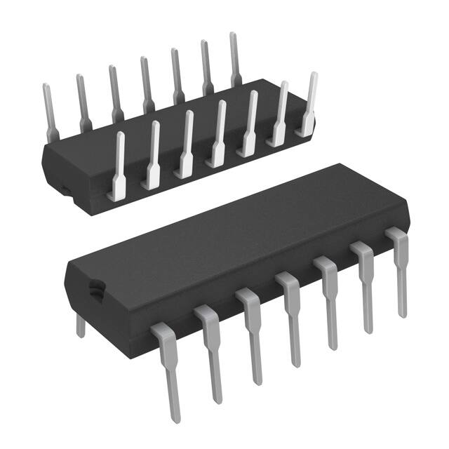
7. 封装信息:
- 提供了Plastic DIP14和SO14两种封装方式的详细机械尺寸数据。