®
74ACT273
OCTAL D-TYPE FLIP FLOP WITH CLEAR
PRELIMINARY DATA
s
s
s
s
s
s
s
s
s
HIGH SPEED: fMAX = 190 MHz ns (TYP.) at VCC = 5V LOW POWER DISSIPATION: ICC = 8 µA (MAX.) at TA = 25 oC COMPATIBLE WITH TTL OUTPUTS VIH = 2V (MIN), VIL = 0.8V (MAX) 50Ω TRANSMISSION LINE DRIVING CAPABILITY SYMMETRICAL OUTPUT IMPEDANCE: |IOH| = IOL = 24 mA (MIN) BALANCED PROPAGATION DELAYS: tPLH ≅ tPHL OPERATING VOLTAGE RANGE: VCC (OPR) = 4.5V to 5.5V PIN AND FUNCTION COMPATIBLE WITH 74 SERIES 273 IMPROVED LATCH-UP IMMUNITY
M (Micro Package) B (Plastic Package) ORDER CODES : 74ACT273B 74ACT273M 74ACT273T T (TSSOP Package)
DESCRIPTION The ACT273 is a high-speed CMOS OCTAL D-TYPE FLIP FLOP WITH CLEAR fabricated with sub-micron silicon gate and double-layer metal wiring C2MOS technology. It is ideal for low power applications mantaining high speed operation similar to equivalent Bipolar Schottky TTL.
Information signals applied to D inputs are transfered to the Q output on the positive going edge of the clock pulse. When the CLEAR input is held low, the Q outputs are held low independentely of the other inputs . The device is designed to interface directly High Speed CMOS systems with TTL, NMOS and CMOS output voltage levels. All inputs and outputs are equipped with protection circuits against static discharge, giving them 2KV ESD immunity and transient excess voltage.
PIN CONNECTION AND IEC LOGIC SYMBOLS
May 1999
1/11
�74ACT273
INPUT AND OUTPUT EQUIVALENT CIRCUIT PIN DESCRIPTION
PIN No 1 2, 5, 6, 9, 12, 15, 16, 19 3, 4, 7, 8, 13, 14, 17, 18 11 SYMBOL CLEAR Q0 to Q7 D0 to D7 CLOCK NAME AND FUNCT ION Asyncronous Master Reset (Active LOW) Flip-Flop Outpus Data Inputs Clock Input (LOW-to-HIGH, EdgeTriggered) Ground (0V) Positive Supply Voltage
10 20
GND VCC
TRUTH TABLE
INPUTS CL EAR L H H H
X:Don’t Care
OUT PUT S CLO CK X Q L L H Qn
F UNCTIO N CLEAR
D X L H X
NO CHANGE
LOGIC DIAGRAMS
Thislogic diagram has notbe used to esimate propagation delays
2/11
�74ACT273
ABSOLUTE MAXIMUM RATINGS
Symbol VCC VI VO IIK IOK IO ICC orIGND Tstg TL Supply Voltage DC Input Voltage DC Output Voltage DC Input Diode Current DC Output Diode Current DC Output Current DC VCC or Ground Current Storage Temperature Lead Temperature (10 sec) Parameter Value -0.5 to +7 -0.5 to VCC + 0.5 -0.5 to VCC + 0.5 ± 20 ± 20 ± 50 ± 400 -65 to +150 300 Unit V V V mA mA mA mA
o o
C C
Absolute Maximum Ratings are those values beyond which damage to the device may occur. Functional operation under these condition is not implied.
RECOMMENDED OPERATING CONDITIONS
Symbol VCC VI VO Top dt/dv Supply Voltage Input Voltage Output Voltage Operating Temperature: Input Rise and Fall Time VCC = 4.5 to 5.5V (note 1) Parameter Value 4.5 to 5.5 0 to VCC 0 to VCC -40 to +85 8 Unit V V V
o
C
ns/V
1) VIN from 0.8 V to 2.0 V
3/11
�74ACT273
DC SPECIFICATIONS
Symb ol Parameter V CC (V) VIH VIL VOH High Level Input Voltage Low Level Input Voltage High Level Output Voltage 4.5 5.5 4.5 5.5 4.5 5.5 4.5 5.5 VOL Low Level Output Voltage 4.5 5.5 4.5 5.5 II ICCT ICC IOLD IOHD Input Leakage Current Max ICC /Input Quiescent Supply Current Dynamic Output Current (note 1, 2) 5.5 5.5 5.5 5.5 VI = VIH or VIL
(*)
Test Co nditions Min. VO = 0.1 V or VCC - 0.1 V VO = 0.1 V or VCC - 0.1 V VI(*) = VIH or VIL IO=-50 µA IO=-50 µA IO=-24 mA IO=-24 mA IO=50 µA IO=50 mA IO=24 mA IO=24 mA VI = VCC orGND VI = VCC -2.1V VI = VCC orGND VOLD = 1.65 V max VOHD = 3.85 V min 0.6 4.4 5.4 3.86 4.86 0.001 0.001 2.0 2.0 T yp. 1.5 1.5 1.5 1.5 4.49 5.49
Valu e T A = 25 oC Max. -40 to 85 o C Min. 2.0 2.0 0.8 0.8 4.4 5.4 3.76 4.76 0.1 0.1 0.36 0.36 ±0.1 4 0.1 0.1 0.44 0.44 ±1 1.5 40 75 -75 0.8 0.8 Max.
Un it
V V V
V
µA mA µA mA mA
1) Maximum test duration 2ms, one output loaded attime 2) Incident wave switching is guaranteed on transmission lines with impedances as low as 50 Ω.
4/11
�74ACT273
AC ELECTRICAL CHARACTERISTICS (CL = 50 pF, RL = 500 Ω, Input tr = tf =3 ns)
Symb ol Parameter V CC (V) tPLH tPHL tPLH tPHL twL tw ts th tREM fMAX Propagation Delay Time CK to Q Propagation Delay Time CLR to Q CLR pulse Width, LOW CK pulse Width Setup Time Q to CK HIGH or LOW Hold Time Q to CK HIGH or LOW Recovery Time CLR to CK Maximum Clock Frequency 5.0(*) 5.0
(*)
T est Con ditio n
Valu e T A = 25 oC -40 to 85 o C Min. T yp. Max. Min. Max. 1.5 6.5 8.5 1.5 9.0 1.5 7.0 1.5 1.0 1.0 -0.5 0.5 125 190 9.0 4.0 4.0 3.5 1.5 3.0 110 1.5 9.5 4.0 4.0 3.5 1.5 3.0
Un it
ns ns ns ns ns ns ns MHz
5.0 5.0
(*) (*)
5.0(*) 5.0(*) 5.0
(*)
5.0(*)
(*) Voltage range is 5V ± 0.5V
CAPACITIVE CHARACTERISTICS
Symb ol Parameter V CC (V) CIN CPD Input Capacitance Power Dissipation Capacitance (note 1) 5.0 5.0 fIN = 10 MHz Test Co nditions Min. T yp. 4 32 Valu e T A = 25 oC Max. -40 to 85 o C Min. Max. pF pF Un it
1) CPD isdefined as the value of the IC’sinternal equivalent capacitance which is calculated fromthe operating current consumption without load. (Referto Test Circuit).Average operting current can be obtained by the following equation. ICC(opr) = CPD • VCC • fIN + ICC/n(per circuit)
5/11
�74ACT273
TEST CIRCUIT
CL = 50 pF or equivalent (includes jigand probe capacitance) RL = R1 = 500Ω orequivalent RT = ZOUT of pulse generator (typically 50Ω)
WAVEFORM 1: PROPAGATION DELAYS, SETUP AND HOLD TIMES (f=1MHz; 50% duty cycle)
6/11
�74ACT273
WAVEFORM 2: PROPAGATION DELAYS (f=1MHz; 50% duty cycle)
WAVEFORM 3: RECOVERY TIME (f=1MHz; 50% duty cycle)
7/11
�74ACT273
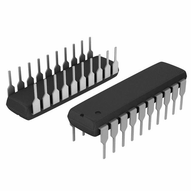
Plastic DIP-20 (0.25) MECHANICAL DATA
mm MIN. a1 B b b1 D E e e3 F I L Z 3.3 1.34 8.5 2.54 22.86 7.1 3.93 0.130 0.053 0.254 1.39 0.45 0.25 25.4 0.335 0.100 0.900 0.280 0.155 1.65 TYP. MAX. MIN. 0.010 0.055 0.018 0.010 1.000 0.065 inch TYP. MAX.
DIM.
P001J
8/11
�74ACT273
SO-20 MECHANICAL DATA
DIM. MIN. A a1 a2 b b1 C c1 D E e e3 F L M S 7.40 0.50 12.60 10.00 1.27 11.43 7.60 1.27 0.75 8 (max.) 0.291 0.19 13.00 10.65 0.35 0.23 0.50 45 (typ.) 0.496 0.393 0.050 0.450 0.299 0.050 0.029 0.512 0.419 0.10 mm TYP. MAX. 2.65 0.20 2.45 0.49 0.32 0.013 0.009 0.020 0.004 MIN. inch TYP. MAX. 0.104 0.007 0.096 0.019 0.012
P013L
9/11
�74ACT273
TSSOP20 MECHANICAL DATA
mm MIN. A A1 A2 b c D E E1 e K L 0o 0.50 0.05 0.85 0.19 0.09 6.4 6.25 4.3 6.5 6.4 4.4 0.65 BSC 4o 0.60 8o 0.70 0o 0.020 0.10 0.9 TYP. MAX. 1.1 0.15 0.95 0.30 0.2 6.6 6.5 4.48 0.002 0.335 0.0075 0.0035 0.252 0.246 0.169 0.256 0.252 0.173 0.0256 BSC 4o 0.024 8o 0.028 0.004 0.354 MIN. inch TYP. MAX. 0.433 0.006 0.374 0.0118 0.0079 0.260 0.256 0.176
DIM.
A
A2 A1 b e K c L E
D
E1
PIN 1 IDENTIFICATION
1
10/11
�74ACT273
Information furnished is believed to be accurate and reliable. However, STMicroelectronics assumes no responsibility for the consequences of use of such information nor for any infringement of patents or other rights of third parties which may result from its use. No license is granted by implication or otherwise under any patent or patent rights of STMicroelectronics. Specification mentioned in this publication are subject to change without notice. This publication supersedes and replaces all information previously supplied. STMicroelectronics products are not authorized for use as critical components in life support devices or systems without express written approval of STMicroelectronics. The ST logo is a trademark of STMicroelectronics © 1999 STMicroelectronics – Printed in Italy – All Rights Reserved STMicroelectronics GROUP OF COMPANIES Australia - Brazil - Canada - China - France - Germany - Italy - Japan - Korea - Malaysia - Malta - Mexico - Morocco - The Netherlands Singapore - Spain - Sweden - Switzerland - Taiwan - Thailand - United Kingdom - U.S.A. http://www.st.com .
11/11
�
很抱歉,暂时无法提供与“74ACT273B”相匹配的价格&库存,您可以联系我们找货
免费人工找货