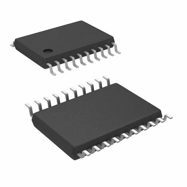
74LCX240TTR

74LCX240TTR

  • 厂商:

    STMICROELECTRONICS(意法半导体)

  • 封装:

    TSSOP20_6.5X4.4MM

  • 描述:

    IC BUFFER INVERT 3.6V 20TSSOP

  • 详情介绍
  • 数据手册
  • 价格&库存
74LCX240TTR 数据手册
74LCX240 LOW VOLTAGE CMOS OCTAL BUS BUFFER (3-STATE INV.) WITH 5V TOLERANT INPUTS AND OUTPUTS s s s s s s s s s s 5V TOLERANT INPUTS AND OUTPUTS HIGH SPEED: tPD = 6.5 ns (MAX.) at VCC = 3V POWER DOWN PROTECTION ON INPUTS AND OUTPUTS SYMMETRICAL OUTPUT IMPEDANCE: |IOH| = IOL = 24mA (MIN) at VCC = 3V PCI BUS LEVELS GUARANTEED AT 24 mA BALANCED PROPAGATION DELAYS: tPLH ≅ tPHL OPERATING VOLTAGE RANGE: VCC(OPR) = 2.0V to 3.6V (1.5V Data Retention) PIN AND FUNCTION COMPATIBLE WITH 74 SERIES 240 LATCH-UP PERFORMANCE EXCEEDS 500mA (JESD 17) ESD PERFORMANCE: HBM > 2000V (MIL STD 883 method 3015); MM > 200V SOP TSSOP Table 1: Order Codes PACKAGE SOP TSSOP T&R 74LCX240MTR 74LCX240TTR DESCRIPTION The 74LCX240 is a low voltage CMOS OCTAL BUS BUFFER fabricated with sub-micron silicon gate and double-layer metal wiring C2MOS technology. It is ideal for low power and high speed 3.3V applications; it can be interfaced to 5V signal environment for both inputs and outputs. It has same speed performance at 3.3V than 5V AC/ACT family, combined with a lower power consumption. This device is designed to be used with 3 state memory address drivers, etc. All inputs and outputs are equipped with protection circuits against static discharge, giving them 2KV ESD immunity and transient excess voltage. Figure 1: Pin Connection And IEC Logic Symbols September 2004 Rev. 6 1/12 74LCX240 Figure 2: Input And Output Equivalent Circuit Table 2: Pin Description PIN N° 1 2, 4, 6, 8 9, 7, 5, 3 11, 13, 15, 17 18, 16, 14, 12 19 10 20 SYMBOL 1G 1A1 to 1A4 2Y1 to 2Y4 2A1 to 2A4 1Y1 to 1Y4 2G GND VCC NAME AND FUNCTION Output Enable Input Data Inputs Data Outputs Data Inputs Data Outputs Output Enable Input Ground (0V) Positive Supply Voltage Table 3: Truth Table INPUT G L L H X : Don’t Care Z : High Impedance OUTPUT An L H X Yn H L Z Table 4: Absolute Maximum Ratings Symbol VCC VI VO VO IIK IOK IO ICC IGND Tstg TL Supply Voltage DC Input Voltage DC Output Voltage (OFF State) DC Output Voltage (High or Low State) (note 1) DC Input Diode Current DC Output Diode Current (note 2) DC Output Current DC Supply Current per Supply Pin DC Ground Current per Supply Pin Storage Temperature Lead Temperature (10 sec) Parameter Value -0.5 to +7.0 -0.5 to +7.0 -0.5 to +7.0 -0.5 to VCC + 0.5 - 50 - 50 ± 50 ± 100 ± 100 -65 to +150 300 Unit V V V V mA mA mA mA mA °C °C Absolute Maximum Ratings are those values beyond which damage to the device may occur. Functional operation under these conditions is not implied 1) IO absolute maximum rating must be observed 2) VO < GND 2/12 74LCX240 Table 5: Recommended Operating Conditions Symbol VCC VI VO VO IOH, IOL IOH, IOL Top dt/dv Supply Voltage (note 1) Input Voltage Output Voltage (OFF State) Output Voltage (High or Low State) High or Low Level Output Current (VCC = 3.0 to 3.6V) High or Low Level Output Current (VCC = 2.7V) Operating Temperature Input Rise and Fall Time (note 2) Parameter Value 2.0 to 3.6 0 to 5.5 0 to 5.5 0 to VCC ± 24 ± 12 -55 to 125 0 to 10 Unit V V V V mA mA °C ns/V 1) Truth Table guaranteed: 1.5V to 3.6V 2) VIN from 0.8V to 2V at VCC = 3.0V Table 6: DC Specifications Test Condition Symbol Parameter VCC (V) -40 to 85 °C Min. 2.0 2.7 to 3.6 0.8 2.7 to 3.6 2.7 3.0 VOL Low Level Output Voltage 2.7 to 3.6 2.7 3.0 II Ioff IOZ Input Leakage Current Power Off Leakage Current High Impedance Output Leakage Current Quiescent Supply Current ICC incr. per Input 2.7 to 3.6 0 2.7 to 3.6 IO=-100 µA IO=-12 mA IO=-18 mA IO=-24 mA IO=100 µA IO=12 mA IO=16 mA IO=24 mA VI = 0 to 5.5V VI or VO = 5.5V VI = VIH or VIL VO = 0 to VCC VI = VCC or GND VI or VO= 3.6 to 5.5V VIH = VCC - 0.6V VCC-0.2 2.2 2.4 2.2 0.2 0.4 0.4 0.55 ±5 10 ±5 10 ± 10 500 VCC-0.2 2.2 2.4 2.2 0.2 0.4 0.4 0.55 ±5 10 ±5 10 ± 10 500 µA µA µA µA µA V V 0.8 V Max. Value -55 to 125 °C Min. 2.0 Max. V Unit VIH VIL VOH High Level Input Voltage Low Level Input Voltage High Level Output Voltage ICC ∆ICC 2.7 to 3.6 2.7 to 3.6 3/12 74LCX240 Table 7: Dynamic Switching Characteristics Test Condition Symbol Parameter VCC (V) 3.3 CL = 50pF VIL = 0V, VIH = 3.3V Value TA = 25 °C Min. Typ. 0.8 -0.8 Max. V Unit VOLP VOLV Dynamic Low Level Quiet Output (note 1) 1) Number of outputs defined as "n". Measured with "n-1" outputs switching from HIGH to LOW or LOW to HIGH. The remaining output is measured in the LOW state. Table 8: AC Electrical Characteristics Test Condition Symbol Parameter VCC (V) 2.7 3.0 to 3.6 2.7 3.0 to 3.6 2.7 3.0 to 3.6 3.0 to 3.6 CL (pF) 50 50 50 50 RL (Ω ) 500 500 500 500 ts = tr (ns) 2.5 2.5 2.5 2.5 -40 to 85 °C Min. 1.5 1.5 1.5 1.5 1.5 1.5 Max. 7.5 6.5 9.0 8.0 8.0 7.0 1.0 Value -55 to 125 °C Min. 1.5 1.5 1.5 1.5 1.5 1.5 Max. 8.5 7.5 10.5 9.2 9.2 8.3 1.0 ns ns ns ns Unit tPLH tPHL tPZL tPZH tPLZ tPHZ tOSLH tOSHL Propagation Delay Time Output Enable Time Output Disable Time Output To Output Skew Time (note1, 2) 1) Skew is defined as the absolute value of the difference between the actual propagation delay for any two outputs of the same device switching in the same direction, either HIGH or LOW (tOSLH = | tPLHm - tPLHn|, tOSHL = | tPHLm - tPHLn|) 2) Parameter guaranteed by design Table 9: Capacitive Characteristics Test Condition Symbol Parameter VCC (V) 3.3 3.3 3.3 VIN = 0 to VCC VIN = 0 to VCC fIN = 10MHz VIN = 0 or VCC Value TA = 25 °C Min. Typ. 6 10 40 Max. pF pF pF Unit CIN COUT CPD Input Capacitance Output Capacitance Power Dissipation Capacitance (note 1) 1) CPD is defined as the value of the IC’s internal equivalent capacitance which is calculated from the operating current consumption without load. (Refer to Test Circuit). Average operating current can be obtained by the following equation. ICC(opr) = CPD x VCC x fIN + ICC/8 (per circuit) 4/12 74LCX240 Figure 3: Test Circuit TEST tPLH, tPHL tPZL, tPLZ tPZH, tPHZ CL = 50 pF or equivalent (includes jig and probe capacitance) RL = R1 = 500Ω or equivalent RT = ZOUT of pulse generator (typically 50Ω) SWITCH Open 6V GND Figure 4: Waveform - Propagation Delays (f=1MHz; 50% duty cycle) 5/12 74LCX240 Figure 5: Waveform - Output Enable And Disable Time (f=1MHz; 50% duty cycle) 6/12 74LCX240 SO-20 MECHANICAL DATA DIM. A A1 B C D E e H h L k ddd 10.00 0.25 0.4 0° mm. MIN. 2.35 0.1 0.33 0.23 12.60 7.4 1.27 10.65 0.75 1.27 8° 0.100 0.394 0.010 0.016 0° TYP MAX. 2.65 0.30 0.51 0.32 13.00 7.6 MIN. 0.093 0.004 0.013 0.009 0.496 0.291 0.050 0.419 0.030 0.050 8° 0.004 inch TYP. MAX. 0.104 0.012 0.020 0.013 0.512 0.299 0016022D 7/12 74LCX240 TSSOP20 MECHANICAL DATA mm. DIM. MIN. A A1 A2 b c D E E1 e K L 0˚ 0.45 0.60 0.05 0.8 0.19 0.09 6.4 6.2 4.3 6.5 6.4 4.4 0.65 BSC 8˚ 0.75 0˚ 0.018 0.024 1 TYP MAX. 1.2 0.15 1.05 0.30 0.20 6.6 6.6 4.48 0.002 0.031 0.007 0.004 0.252 0.244 0.169 0.256 0.252 0.173 0.0256 BSC 8˚ 0.030 0.004 0.039 MIN. TYP. MAX. 0.047 0.006 0.041 0.012 0.0079 0.260 0.260 0.176 inch A A2 A1 b e K c L E D E1 PIN 1 IDENTIFICATION 1 0087225C 8/12 74LCX240 Tape & Reel SO-20 MECHANICAL DATA mm. DIM. MIN. A C D N T Ao Bo Ko Po P 10.8 13.2 3.1 3.9 11.9 12.8 20.2 60 30.4 11 13.4 3.3 4.1 12.1 0.425 0.520 0.122 0.153 0.468 TYP MAX. 330 13.2 0.504 0.795 2.362 1.197 0.433 0.528 0.130 0.161 0.476 MIN. TYP. MAX. 12.992 0.519 inch 9/12 74LCX240 Tape & Reel TSSOP20 MECHANICAL DATA mm. DIM. MIN. A C D N T Ao Bo Ko Po P 6.8 6.9 1.7 3.9 11.9 12.8 20.2 60 22.4 7 7.1 1.9 4.1 12.1 0.268 0.272 0.067 0.153 0.468 TYP MAX. 330 13.2 0.504 0.795 2.362 0.882 0.276 0.280 0.075 0.161 0.476 MIN. TYP. MAX. 12.992 0.519 inch 10/12 74LCX240 Table 10: Revision History Date 15-Sep-2004 Revision 6 Description of Changes Ordering Codes Revision - pag. 1. 11/12 74LCX240 Information furnished is believed to be accurate and reliable. However, STMicroelectronics assumes no responsibility for the consequences of use of such information nor for any infringement of patents or other rights of third parties which may result from its use. No license is granted by implication or otherwise under any patent or patent rights of STMicroelectronics. Specifications mentioned in this publication are subject to change without notice. This publication supersedes and replaces all information previously supplied. STMicroelectronics products are not authorized for use as critical components in life support devices or systems without express written approval of STMicroelectronics. The ST logo is a registered trademark of STMicroelectronics All other names are the property of their respective owners © 2004 STMicroelectronics - All Rights Reserved STMicroelectronics group of companies Australia - Belgium - Brazil - Canada - China - Czech Republic - Finland - France - Germany - Hong Kong - India - Israel - Italy - Japan Malaysia - Malta - Morocco - Singapore - Spain - Sweden - Switzerland - United Kingdom - United States of America www.st.com 12/12
74LCX240TTR
1. 物料型号: - SOP封装:74LCX240MTR - TSSOP封装:74LCX240TTR

2. 器件简介: - 74LCX240是一款低压CMOS八路总线缓冲器(3态反相),具备5V容限输入输出,高速性能(最大传播延迟6.5ns),电源关闭保护以及对称输出阻抗。

3. 引脚分配: - 1G:输出使能输入 - 1A1至1A4:数据输入 - 2Y1至2Y4:数据输出 - 2A1至2A4:数据输入 - 1Y1至1Y4:数据输出 - 2G:输出使能输入 - GND:地(0V) - Vcc:正电源电压

4. 参数特性: - 工作电压范围:2.0V至3.6V(1.5V数据保持) - 对称输出阻抗:|I_OH|=I_OL=24mA(最小值)在3V电源下 - ESD性能:HBM > 2000V(MIL STD 883方法3015); MM > 200V

5. 功能详解: - 所有输入输出均配备有防静电放电保护电路,提供2KV的ESD保护和瞬态过电压保护。 - 设计用于与3态存储器地址驱动器等配合使用。

6. 应用信息: - 适用于低功耗、高速3.3V应用,可以与5V信号环境进行双向接口。

7. 封装信息: - 提供SOIC-20和TSSOP-20两种封装方式,详细机械尺寸数据已在文档中给出。

74LCX240TTR 价格&库存

很抱歉,暂时无法提供与“74LCX240TTR”相匹配的价格&库存,您可以联系我们找货

免费人工找货