74LVTH16244
LOW VOLTAGE BICMOS 16 BIT BUS BUFFER
WITH BUS HOLD AND POWER UP 3-STATE
■
■
HIGH SPEED:
tPD = 3.2ns (MAX.) at TA = 85°C VCC = 3.0V
LOW POWER DISSIPATION HIGH LEVEL
OUTPUT: ICC = 190µA (MAX.) at TA = 85°C
OUTPUT IMPEDANCE:
|IOH| = 32mA, IOL = 64mA (MIN at VCC = 3.0V)
|IOH| = 8mA, IOL = 24mA (MIN at VCC = 2.7V)
BALANCED PROPAGATION DELAYS:
tPLH ≅ tPHL
POWER DOWN PROTECTION ON INPUTS
AND OUTPUTS
COMPATIBLE WITH TTL OUTPUTS:
VIH = 2V (MIN),VIL = 0.8V(MAX) at
VCC = 2.7 to 3.6V
POWER-UP/DOWN 3-STATE: IOZPU = 100µA
MAX at VCC = 0V to 1.5V, VCC = 1.5V to 0V, TA
= 85°C
BUS HOLD PROVIDED ON DATA INPUTS
OPERATING VOLTAGE RANGE:
VCC(OPR) = 2.7V to 3.6V
PIN AND FUNCTION COMPATIBLE WITH
74 SERIES H16244
LATCH-UP PERFORMANCE EXCEEDS
500mA (JESD 17)
)
s
(
t
c
u
d
o
)
r
s
(
P
t
c
e
t
u
e
d
l
o
o
r
s
P
b
e
O
t
e
l
)
o
s
(
s
t
b
c
u
O
d
o
)
r
s
P
(
t
c
e
t
u
e
l
d
o
o
r
s
P
b
O
e
t
e
l
o
s
b
O
■
■
■
■
■
■
■
■
■
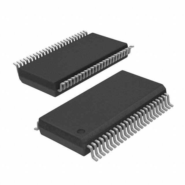
TSSOP
TFBGA
ORDER CODES
PACKAGE
T&R
TSSOP48
TFBGA54
74LVTH16244TTR
74LVTH16244LBR
LOGIC DIAGRAM
DESCRIPTION
The 74LVTH16244 is a low voltage BiCMOS 16
BIT BUS BUFFER (NON-INVERTED) fabricated
with sub-micron silicon gate and five-layer metal
wiring BiCMOS technology. It is ideal and full
specified for hot-insertion and high speed 3.3V applications; the power-up/down 3-state circuitry
places the outputs in the high impedance state
during power-up/down, which prevents driver conflict. This function is guaranteed when VCC is between 0 and 1.5V. It can be interfaced to 3.3V signal environment for both inputs and outputs. Any
nG output control governs four BUS BUFFERS.
Output Enable input (nG) tied together gives full
16-bit operation. When nG is LOW, the outputs
are on. When nG is HIGH, the output are in high
impedance state effectively isolated. Bus hold on
data inputs is provided in order to eliminate the
need for external pull-up or pull-down resistors.
All inputs and outputs are equipped with protection circuits against static discharge, giving them
ESD immunity and transient excess voltage.
February 2004
1/13
�74LVTH16244
INPUT AND OUTPUT EQUIVALENT CIRCUIT
)
s
(
t
c
u
d
o
)
r
s
(
P
t
c
e
t
u
e
d
l
o
o
r
s
P
b
e
O
t
e
l
)
o
s
(
s
t
b
c
u
O
d
o
)
r
s
P
(
t
c
e
t
u
e
l
d
o
o
r
s
P
b
O
e
t
e
l
o
s
b
O
PIN DESCRIPTION
TFBGA PIN No
TSSOP PIN No
SYMBOL
A3, J3
A6, B5, B6, C5, C6, D5, D6, E5, E6,
F5, F6, G5, G6, H5, H6, J6
A1, B2, B1, C2, C1, D2, D1, E2, E1,
F2, F1, G2, G1, H2, H1, J1
J4, A4
D3, D4, E3, E4, F3, F4
A2, A5, B3, B4, H3, H4, J2, J5
C4, G4, C3, G3
1, 24
47, 46, 44, 43, 41, 40, 38, 37,
36, 35, 33, 32, 30, 29, 27, 26
2, 3, 5, 6, 8, 9, 11, 12,
13, 14, 16, 17, 19, 20, 22, 23
25, 48
4, 10, 15, 21, 28, 34, 39, 45
42, 31, 7, 18
1G, 4G
1A1-4,2A1-4
3A1-4, 4A1-4
1Y1-4,2Y1-4
3Y1-4, 4Y1-4
3G, 2G
GND
NC
VCC
2/13
NAME AND FUNCTION
Output Enable Inputs
Data Inputs
Data Outputs
Output Enable Inputs
Ground (0V)
No Connected
Positive Supply Voltage
�74LVTH16244
PIN CONNECTION (top view for TSSOP, top through view for BGA)
TSSOP
TFBGA
)
s
(
t
c
u
d
o
)
r
s
(
P
t
c
e
t
u
e
d
l
o
o
r
s
P
b
e
O
t
e
l
)
o
s
(
s
t
b
c
u
O
d
o
)
r
s
P
(
t
c
e
t
u
e
l
d
o
o
r
s
P
b
O
e
t
e
l
o
s
b
O
TRUTH TABLE
INPUTS
OUTPUT
nG
xAn
xYn
L
L
H
L
H
X
L
H
Z
Z = High Impedance; X = Don’t care, n = 1..4, x = 1..4
3/13
�74LVTH16244
ABSOLUTE MAXIMUM RATINGS
Symbol
VCC
Parameter
Value
Unit
Supply Voltage
-0.5 to +4.6
V
VI
DC Input Voltage
-0.5 to +4.6
V
VO
DC Output Voltage (Output disabled)
VO
DC Output Voltage
-0.5 to +4.6
V
-0.5 to VCC + 0.5
− 50
V
mA
IIK
DC Input Diode Current
IOK
DC Output Diode Current
− 50
mA
128
mA
64
mA
IO
DC Output Current low state
IO
DC Output Current high state
ICC
DC VCC or Ground Current
Pd
Power Dissipation (*)
400
Tstg
Storage Temperature
-65 to +150
TL
Lead Temperature (10 sec)
)
s
(
t
± 100
c
u
d
300
o
r
P
mA
mW
°C
°C
)
s
t(
Absolute Maximum Ratings are those values beyond which damage to the device may occur. Functional operation under these conditions is
not implied
(*) 500mW: ≅ 65°C derated to 300mW by 10mW/°C: 65°C to 85°C
e
t
e
l
RECOMMENDED OPERATING CONDITIONS
Symbol
VCC
Supply Voltage
VI
Input Voltage (An, nG)
VO
Output Voltage
VO
Output Voltage (Output Disabled)
Top
Operating Temperature
dt/dVCC
dt/dv
du
Minimum Power-up ramp rate
Input Rise and Fall Time (note 1)
e
t
e
ol
o
r
P
)
s
(
ct
4/13
u
d
o
r
P
e
t
e
l
o
s
b
O
)-
s
(
t
c
1) VI from 0.8V to 2.0V at VCC =2.7V to 3.6V
s
b
O
so
Parameter
b
O
b
O
-
so
e
t
le
c
u
d
o
r
P
Value
Unit
2.7 to 3.6
V
0 to 3.6
V
VCC
V
3.6
V
-40 to 85
°C
200
µs/V
0 to 20
ns/V
�74LVTH16244
DC SPECIFICATIONS
Test Condition
Symbol
VIK
Parameter
VIL
Low Level Input Voltage
(An, nG)
II
Control Input Leakage
Current
Data Input Leakage
Current
II(HOLD) Data Input Hold Current
High Level Output
Voltage
VOH
VOL
TA = 25 °C
VCC
(V)
Input Voltage Clamp
(An, nG)
High Level Input Voltage
(An, nG)
VIH
Low Level Output
Voltage
Min.
IIK = -18mA
2.7
0.8
0.8
135
VI = 2.0V
-135
3.6
VI = 0 to 3.6V
2.7
IO = -100 µA
2.7
IO = -8 mA
3.0
IO = -32 mA
2.7
IO = 100 µA
2.7
IO = 24 mA
)-
IOFF
ICCA
O
∆ICC
V
V
(s)
t
c
u
so
e
t
le
so
IO = 32 mA
b
O
-
od
75
Pr
-75
o
r
P
µA
µA
)
s
t(
± 500
c
u
d
2.5
µA
2.4
µA
V
2.0
0.2
0.5
0.4
V
0.5
0.55
µA
VO = 0.5V or 3.0V
VI = GND or VCC
nG = GND or VCC
± 100
µA
High Impedance Output 1.5 to 0
Leakage Current
VO = 0.5V or 3.0V
VI = GND or VCC
nG = GND or VCC
± 100
µA
Power Off Leakage
Current
0
VI = GND to 3.6V
VO = GND to 3.6V
± 100
µA
3.6
VO = High, IO = 0
0.19
mA
o
r
P
3.6
u
d
o
r
P
e
Quiescent Supply
Current
Maximum Quiescent
Supply Current / Input
(An or nG)
VO = 0.5V or 3.0V
VI = VIL or VIH
nG = VCC
)
s
(
ct
High Impedance Output 0 to 1.5
Leakage Current
t
e
l
o
bs
2.0
2.0
±5
e
t
e
ol
s
b
O
e
t
e
l
b
O
IO = 64 mA
V
±1
IO = 16 mA
t(s
-1.2
±1
3.0
Unit
Max.
0.8
0.8
3.0
c
u
d
High Impedance Output
Leakage Current
IOZPD
Min.
2.0
2.0
VI = GND or VCC
nG = GND
VI = 0.8V
3.6
3.0
Max.
VI = GND or VCC
3.6
3.0
IOZPU
Typ.
-40 to 85 °C
-0.85
2.7
3.3 (*)
2.7
3.3 (*)
3.0
IOZ
Value
3.3 (*)
VO = Low, IO = 0
5.0
nG = VCC, IO = 0
VO = GND or VCC
0.19
VI = VCC - 0.6V
An,nG = VCC or GND
0.2
mA
(*) Power Supply Range VCC = 3.3±0.3V
5/13
�74LVTH16244
AC ELECTRICAL CHARACTERISTICS
Value
Symbol
Parameter
Test Condition
tPLH
Propagation Delay Time An to Yn
TA = - 40 to 85 °C
tPHL
VCC = 3.3 ± 0.3V
VCC = 2.7V
Min.
Unit
Max.
Min.
Typ.
Max.
3.7
1.2
2.5
3.2
ns
Propagation Delay Time An to Yn
3.7
1.2
2.5
3.2
ns
tPZL
Output Enable Time nG to Yn
5.0
1.2
2.7
4.0
ns
tPZH
Output Enable Time nG to Yn
5.0
1.2
2.7
4.0
ns
ns
tPLZ
Output Disable Time nG to Yn
4.4
2.0
3.7
4.2
tPHZ
Output Disable Time nG to Yn
5.0
2.2
4.4
5.1
tOSLH
tOSHL
Output To Output Skew Time
(note1, 2)
(s)
ct
0.5
u
d
o
ns
ns
1) Skew is defined as the absolute value of the difference between the actual propagation delay for any two outputs of the same device
switching in the same direction, either HIGH or LOW (tOSLH = | tPLHm - tPLHn|, tOSHL = | tPHLm - tPHLn|
2) Parameter guaranteed by design
CAPACITANCE CHARACTERISTICS
e
t
e
l
Test Condition
Symbol
Parameter
CI
Control Input Capacitance
CO
Output Capacitance
3.3
s
(
t
c
u
d
o
t
e
l
o
s
b
O
)-
open
TEST CIRCUIT
r
P
e
so
VCC
(V)
)
s
(
ct
Value
o
r
P
TA = 25 °C
Min.
o
s
b
O
-
e
t
le
c
u
d
)
s
t(
Typ.
Max.
-40 to 85 °C
Min.
6
pF
15
pF
u
d
o
t
e
l
o
TEST
tPLH, tPHL
tPZL, tPLZ (VCC = 3.0 to 3.6V)
tPZL, tPLZ (VCC = 2.7V)
tPZH, tPHZ
CL = 50pF or equivalent (includes jig and probe capacitance)
RL = R1 = 500Ω or equivalent
RT = ZOUT of pulse generator (typically 50Ω)
Unit
Max.
r
P
e
s
b
O
6/13
b
O
Pr
SWITCH
Open
6V
6V
GND
�74LVTH16244
WAVEFORM SYMBOL VALUE
VCC
Symbol
VIH
3.0 to 3.6V
2.7V
2.7V
VCC
VM
1.5V
1.5V
VX
VOL +0.3V
VOL +0.15V
VY
VOH -0.3V
VOH -0.15V
WAVEFORM 1: PROPAGATION DELAY (f=1MHz; 50% duty cycle)
)
s
(
t
c
u
d
o
)
r
s
(
P
t
c
e
t
u
e
d
l
o
o
r
s
P
b
e
O
t
e
l
)
o
s
(
s
t
b
c
u
O
d
o
)
r
s
P
(
t
c
e
t
u
e
l
d
o
o
r
s
P
b
O
e
t
e
l
o
s
b
O
7/13
�74LVTH16244
WAVEFORM 2: OUTPUT ENABLE AND DISABLE TIME (f=1MHz; 50% duty cycle)
)
s
(
t
c
u
d
o
)
r
s
(
P
t
c
e
t
u
e
d
l
o
o
r
s
P
b
e
O
t
e
l
)
o
s
(
s
t
b
c
u
O
d
o
)
r
s
P
(
t
c
e
t
u
e
l
d
o
o
r
s
P
b
O
e
t
e
l
o
s
b
O
8/13
�74LVTH16244
TSSOP48 MECHANICAL DATA
mm.
inch
DIM.
MIN.
TYP
MAX.
A
MIN.
TYP.
1.2
A1
0.05
0.047
0.15
A2
MAX.
0.002
0.006
0.9
0.035
)
s
(
t
c
u
d
o
)
r
s
(
P
t
c
e
t
u
e
d
l
o
o
r
s
P
b
e
O
t
e
l
)
o
s
(
s
t
b
c
u
O
d
o
)
r
s
P
(
t
c
e
t
u
e
l
d
o
o
r
s
P
b
O
e
t
e
l
o
s
b
O
b
0.17
0.27
0.0067
0.011
c
0.09
0.20
0.0035
0.0079
D
12.4
12.6
0.488
0.496
E
8.1 BSC
E1
6.0
0.318 BSC
6.2
e
0.236
0.5 BSC
0.244
0.0197 BSC
K
0˚
8˚
0˚
8˚
L
0.50
0.75
0.020
0.030
A
A2
A1
b
K
e
L
E
c
D
E1
PIN 1 IDENTIFICATION
1
7065588C
9/13
�74LVTH16244
TFBGA54 MECHANICAL DATA
mm.
mils
DIM.
MIN.
TYP
A
MAX.
MIN.
TYP.
1.2
A1
0.25
A2
0.78
B
0.35
D
7.9
MAX.
47.2
9.8
0.86
30.7
0.45
13.7
8.1
311.0
33.8
)
s
(
t
c
u
d
o
)
r
s
(
P
t
c
e
t
u
e
d
l
o
o
r
s
P
b
e
O
t
e
l
)
o
s
(
s
t
b
c
u
O
d
o
)
r
s
P
(
t
c
e
t
u
e
l
d
o
o
r
s
P
b
O
e
t
e
l
o
s
b
O
D1
E
0.4
6.4
5.4
5.5
15.7
17.7
318.9
252.0
5.6
212.6
216.5
E1
4
157.5
e
0.8
31.5
SE
0.4
15.7
220.5
7390143/C
10/13
�74LVTH16244
Tape & Reel TSSOP48 MECHANICAL DATA
mm.
inch
DIM.
MIN.
A
TYP
MAX.
MIN.
330
C
12.8
D
20.2
13.2
TYP.
MAX.
12.992
0.504
0.519
0.795
)
s
(
t
c
u
d
o
)
r
s
(
P
t
c
e
t
u
e
d
l
o
o
r
s
P
b
e
O
t
e
l
)
o
s
(
s
t
b
c
u
O
d
o
)
r
s
P
(
t
c
e
t
u
e
l
d
o
o
r
s
P
b
O
e
t
e
l
o
s
b
O
N
60
T
2.362
30.4
1.197
Ao
8.7
8.9
0.343
0.350
Bo
13.1
13.3
0.516
0.524
Ko
1.5
1.7
0.059
0.067
Po
3.9
4.1
0.153
0.161
P
11.9
12.1
0.468
0.476
11/13
�74LVTH16244
Tape & Reel TFBGA54 MECHANICAL DATA
mm.
inch
DIM.
MIN.
TYP
A
MAX.
MIN.
TYP.
330
C
12.8
D
20.2
13.2
MAX.
12.992
0.504
0.519
0.795
)
s
(
t
c
u
d
o
)
r
s
(
P
t
c
e
t
u
e
d
l
o
o
r
s
P
b
e
O
t
e
l
)
o
s
(
s
t
b
c
u
O
d
o
)
r
s
P
(
t
c
e
t
u
e
l
d
o
o
r
s
P
b
O
e
t
e
l
o
s
b
O
N
60
2.362
T
12/13
22.4
0.882
Ao
6.1
0.240
Bo
8.6
0.339
Ko
1.8
0.071
Po
3.9
4.1
0.153
0.161
P
7.9
8.1
0.311
0.319
�74LVTH16244
)
s
(
t
c
u
d
o
)
r
s
(
P
t
c
e
t
u
e
d
l
o
o
r
s
P
b
e
O
t
e
l
)
o
s
(
s
t
b
c
u
O
d
o
)
r
s
P
(
t
c
e
t
u
e
l
d
o
o
r
s
P
b
O
e
t
e
l
o
s
b
O
Information furnished is believed to be accurate and reliable. However, STMicroelectronics assumes no responsibility for the
consequences of use of such information nor for any infringement of patents or other rights of third parties which may result from
its use. No license is granted by implication or otherwise under any patent or patent rights of STMicroelectronics. Specifications
mentioned in this publication are subject to change without notice. This publication supersedes and replaces all information
previously supplied. STMicroelectronics products are not authorized for use as critical components in life support devices or
systems without express written approval of STMicroelectronics.
The ST logo is a registered trademark of STMicroelectronics
All other names are the property of their respective owners
© 2004 STMicroelectronics - All Rights Reserved
STMicroelectronics GROUP OF COMPANIES
Australia - Belgium - Brazil - Canada - China - Czech Republic - Finland - France - Germany - Hong Kong - India - Israel - Italy - Japan Malaysia - Malta - Morocco - Singapore - Spain - Sweden - Switzerland - United Kingdom - United States.
http://www.st.com
13/13
�