74V1G80
SINGLE POSITIVE EDGE TRIGGERED D-TYPE FLIP-FLOP
s
s
s
s s
s
s
s
HIGH SPEED: fMAX = 180MHz (TYP.) at VCC = 5V LOW POWER DISSIPATION: ICC = 1µA(MAX.) at TA=25°C HIGH NOISE IMMUNITY: VNIH = V NIL = 28% VCC (MIN.) POWER DOWN PROTECTION ON INPUTS SYMMETRICAL OUTPUT IMPEDANCE: |IOH| = IOL = 8mA (MIN) at VCC = 4.5V BALANCED PROPAGATION DELAYS: tPLH ≅ tPHL OPERATING VOLTAGE RANGE: VCC(OPR) = 2V to 5.5V IMPROVED LATCH-UP IMMUNITY
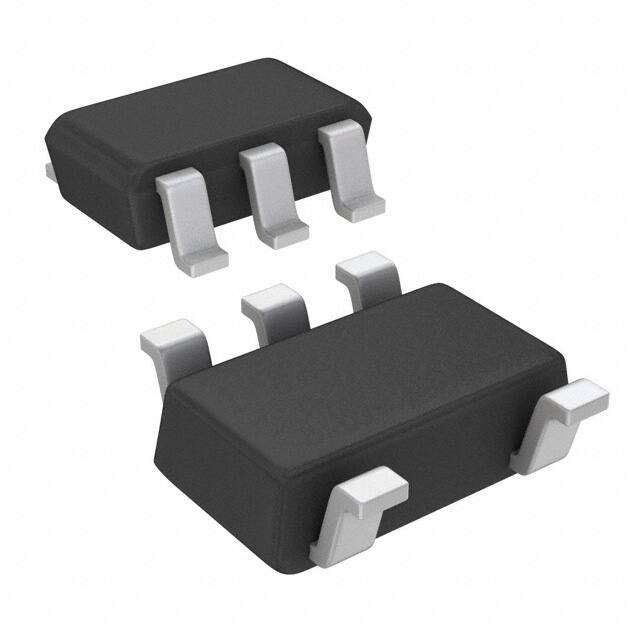
SOT23-5L
SOT323-5L
ORDER CODES
PACKAGE SOT23-5L SOT323-5L T&R 74V1G80STR 74V1G80CTR
DESCRIPTION The 74V1G80 is an advanced high-speed CMOS SINGLE POSITIVE EDGE TRIGGERED D-TYPE FLIP-FLOP WITH INVERTED OUTPUT fabricated with sub-micron silicon gate and double-layer metal wiring C2MOS technology. it is designed to operate from 2V to 5.5V, making this device ideal for portable applications. This D-Type flip-flop is controlled by a clock input (CK). On the positive transition of the clock, the Q output will be set to the logic inverted state that was setup at the D input.
Following the hold time interval, data at the D input can be changed without affecting the level at the output. Power down protection is provided on input and 0 to 7V can be accepted on input with no regard to the supply voltage. This device can be used to interface 5V to 3V. It’s available in the commercial temperature range. All inputs and output are equipped with protection circuits against static discharge, giving them ESD immunity and transient excess voltage.
PIN CONNECTION AND IEC LOGIC SYMBOLS
July 2001
1/10
�74V1G80
INPUT EQUIVALENT CIRCUIT PIN DESCRIPTION
PIN No 1 2 4 3 5 SYMBOL D CK Q GND VCC NAME AND FUNCTION Data Input Clock Input (Positive Edge) Inverted Flip-Flop Output Ground (0V) Positive Supply Voltage
TRUTH TABLE
D L H L H CK Q H L Qn Qn
ABSOLUTE MAXIMUM RATINGS
Symbol VCC VI VO IIK IOK IO Supply Voltage DC Input Voltage DC Output Voltage DC Input Diode Current DC Output Diode Current DC Output Current Parameter Value -0.5 to +7.0 -0.5 to +7.0 -0.5 to VCC + 0.5 - 20 ± 20 ± 25 ± 50 -65 to +150 260 Unit V V V mA mA mA mA °C °C
ICC or IGND DC VCC or Ground Current Tstg Storage Temperature TL Lead Temperature (10 sec)
Absolute Maximum Ratings are those values beyond which damage to the device may occur. Functional operation under these conditions is not implied.
RECOMMENDED OPERATING CONDITIONS
Symbol VCC VI VO Top dt/dv Supply Voltage Input Voltage Output Voltage Operating Temperature Input Rise and Fall Time (note 1) (VCC = 3.3 ± 0.3V) (VCC = 5.0 ± 0.5V) Parameter Value 2 to 5.5 0 to 5.5 0 to VCC -55 to 125 0 to 100 0 to 20 Unit V V V °C ns/V ns/V
1) VIN from 30% to 70% of V CC
2/10
�74V1G80
DC SPECIFICATIONS
Test Condition Symbol Parameter VCC (V) 2.0 3.0 to 5.5 2.0 3.0 to 5.5 2.0 3.0 4.5 3.0 4.5 VOL Low Level Output Voltage 2.0 3.0 4.5 3.0 4.5 II ICC Input Leakage Current Quiescent Supply Current 0 to 5.5 5.5 IO=-50 µA IO=-50 µA IO=-50 µA IO=-4 mA IO=-8 mA IO=50 µA IO=50 µA IO=50 µA IO=4 mA IO=8 mA VI = 5.5V or GND VI = VCC or GND TA = 25°C Min. 1.5 0.7VCC 0.5 0.3VCC 1.9 2.9 4.4 2.58 3.94 0.0 0.0 0.0 0.1 0.1 0.1 0.36 0.36 ± 0.1 1 2.0 3.0 4.5 1.9 2.9 4.4 2.48 3.8 0.1 0.1 0.1 0.44 0.44 ±1 10 Typ. Max. Value -40 to 85°C Min. 1.5 0.7VCC 0.5 0.3VCC 1.9 2.9 4.4 2.4 3.7 0.1 0.1 0.1 0.55 0.55 ±1 20 µA µA V V Max. -55 to 125°C Min. 1.5 0.7VCC 0.5 0.3VCC V V Max. Unit
VIH
High Level Input Voltage Low Level Input Voltage High Level Output Voltage
VIL
VOH
AC ELECTRICAL CHARACTERISTICS (Input tr = tf = 3ns)
Test Condition Symbol Parameter VCC (V) 3.3
(*)
Value TA = 25°C Min. Typ. 4.9 5.9 3.5 4.5 4.0 3.0 4.0 3.0 1.0 1.0 Max. 8.4 12.0 5.6 8.0 -40 to 85°C Min. 1.0 1.0 1.0 1.0 4.0 3.0 4.0 3.0 1.0 1.0 120 180 90 150 Max. 9.8 14.0 7.0 10.0 -55 to 125°C Min. 1.0 1.0 1.0 1.0 4.0 3.0 4.0 3.0 1.0 1.0 90 150 Max. 10.8 15.0 8.0 11.0 ns ns ns Unit
CL (pF) 15 50 15 50
tPLH tPHL Propagation Delay Time CK to Q
3.3(*) 5.0(**) 5.0(**)
tW ts th fMAX
CK Pulse Width, HIGH or LOW Setup Time D to CK, HIGH or LOW Hold Time D to CK, HIGH or LOW Maximum Clock Frequency
3.3 5.0
(*)
(**)
3.3(*) 5.0(**) 3.3(*) 5.0
(**)
ns
3.3(*) 5.0(**)
50 50
100 165
MHz
(*) Voltage range is 3.3V ± 0.3V (**) Voltage range is 5.0V ± 0.5V
3/10
�74V1G80
CAPACITIVE CHARACTERISTICS
Test Condition Symbol Parameter Min. CIN CPD Input Capacitance Power Dissipation Capacitance (note 1) TA = 25°C Typ. 4 8 Max. 10 Value -40 to 85°C Min. Max. 10 -55 to 125°C Min. Max. 10 pF pF Unit
1) CPD is defined as the value of the IC’s internal equivalent capacitance which is calculated from the operating current consumption without load. (Refer to Test Circuit). Average operating current can be obtained by the following equation. ICC(opr) = CPD x VCC x fIN + ICC
TEST CIRCUIT
CL = 15/50pF or equivalent (includes jig and probe capacitance) RT = ZOUT of pulse generator (typically 50Ω)
4/10
�74V1G80
WAVEFORM: PROPAGATION DELAY, SETUP AND HOLD TIMES (f=1MHz; 50% duty cycle)
5/10
�74V1G80
SOT23-5L MECHANICAL DATA
mm. DIM. MIN. A A1 A2 b C D E E1 e e1 L 0.35 0.90 0.00 0.90 0.35 0.09 2.80 2.60 1.50 0.95 1.9 0.55 13.7 TYP MAX. 1.45 0.15 1.30 0.50 0.20 3.00 3.00 1.75 MIN. 35.4 0.0 35.4 13.7 3.5 110.2 102.3 59.0 37.4 74.8 21.6 TYP. MAX. 57.1 5.9 51.2 19.7 7.8 118.1 118.1 68.8 mils
6/10
�74V1G80
SOT323-5L MECHANICAL DATA
mm. DIM. MIN. A A1 A2 b C D E E1 e e1 L 0.10 0.80 0.00 0.80 0.15 0.10 1.80 1.80 1.15 0.65 1.3 0.30 3.9 TYP MAX. 1.10 0.10 1.00 0.30 0.18 2.20 2.40 1.35 MIN. 31.5 0.0 31.5 5.9 3.9 70.9 70.9 45.3 25.6 51.2 11.8 TYP. MAX. 43.3 3.9 39.4 11.8 7.1 86.6 94.5 53.1 mils
7/10
�74V1G80
Tape & Reel SOT23-xL MECHANICAL DATA
mm. DIM. MIN. A C D N T Ao Bo Ko Po P 3.13 3.07 1.27 3.9 3.9 3.23 3.17 1.37 4.0 4.0 12.8 20.2 60 14.4 3.33 3.27 1.47 4.1 4.1 0.123 0.120 0.050 0.153 0.153 0.127 0.124 0.054 0.157 0.157 13.0 TYP MAX. 180 13.2 0.504 0.795 2.362 0.567 0.131 0.128 0.0.58 0.161 0.161 0.512 MIN. TYP. MAX. 7.086 0.519 inch
8/10
�74V1G80
Tape & Reel SOT323-xL MECHANICAL DATA
mm. DIM. MIN. A C D N T Ao Bo Ko Po P 3.98 3.98 2.25 2.7 1.2 4 4 4.2 4.2 0.156 0.156 175 12.8 20.2 59.5 60 60.5 14.4 0.088 0.106 0.047 0.157 0.157 0.165 0.165 TYP 180 13 MAX. 185 13.2 MIN. 6.889 0.504 0.795 2.362 0.567 TYP. 7.086 0.512 MAX. 7.283 0.519 inch
9/10
�74V1G80
Information furnished is believed to be accurate and reliable. However, STMicroelectronics assumes no responsibility for the consequences of use of such information nor for any infringement of patents or other rights of third parties which may result from its use. No license is granted by implication or otherwise under any patent or patent rights of STMicroelectronics. Specifications mentioned in this publication are subject to change without notice. This publication supersedes and replaces all information previously supplied. STMicroelectronics products are not authorized for use as critical components in life support devices or systems without express written approval of STMicroelectronics. © The ST logo is a registered trademark of STMicroelectronics © 2001 STMicroelectronics - Printed in Italy - All Rights Reserved STMicroelectronics GROUP OF COMPANIES Australia - Brazil - China - Finland - France - Germany - Hong Kong - India - Italy - Japan - Malaysia - Malta - Morocco Singapore - Spain - Sweden - Switzerland - United Kingdom © http://www.st.com
10/10
�
很抱歉,暂时无法提供与“74V1G80STR”相匹配的价格&库存,您可以联系我们找货
免费人工找货