1. 物料型号:
- 型号为74V2G66。
2. 器件简介:
- 74V2G66是一款高速CMOS双单刀双掷开关,采用硅门C2MOS技术制造。它具有高速传播延迟和非常低的导通电阻,同时保持真正的CMOS低功耗特性,使其非常适合电池供电设备。
3. 引脚分配:
- 1,5脚:1to21/O,独立输入/输出。
- 2,6脚:1to20/l,独立输出/输入。
- 3,7脚:1Cto2C,使能输入(高电平有效)。
- 4脚:GND,地(0V)。
- 8脚:Vcc,正供电电压。
4. 参数特性:
- 高速:典型值0.3纳秒的传播延迟(5V供电)和0.4纳秒(3.3V供电)。
- 低功耗:25°C时最大1μA的供电电流。
- 低导通电阻:典型值10欧姆(5V供电,输入/输出电流100μA)和12欧姆(3.3V供电)。
- 低失真:3.3V供电时,1kHz下典型值为0.04%。
5. 功能详解:
- 74V2G66能够处理轨到轨的模拟和数字信号,C输入用于控制开关,当C输入为高电平时开关导通,为低电平时关闭。适用于电池供电系统、音频信号路由、通信系统、测试设备等多种应用。
6. 应用信息:
- 适用于电池供电系统、音频信号路由、通信系统、测试设备等。
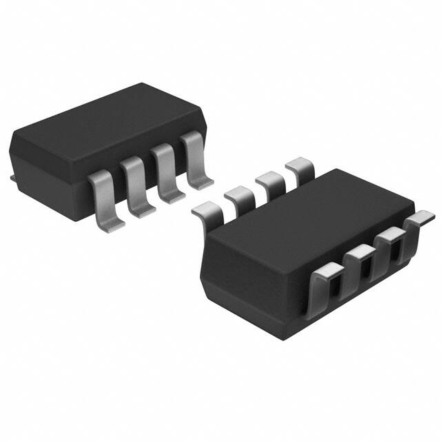
7. 封装信息:
- 提供SOT23-8L封装。