0
登录后你可以
  • 下载海量资料
  • 学习在线课程
  • 观看技术视频
  • 写文章/发帖/加入社区
创作中心
发布
  • 发文章

  • 发资料

  • 发帖

  • 提问

  • 发视频

创作活动
74V2T08STR

74V2T08STR

  • 厂商:

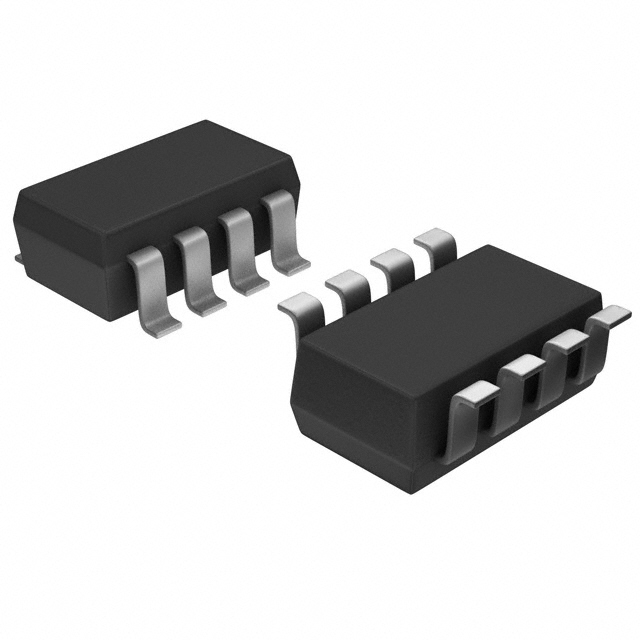
    STMICROELECTRONICS(意法半导体)

  • 封装:

    SOT23-8L

  • 描述:

    IC GATE AND 2CH 2-INP SOT23-8

  • 数据手册
  • 价格&库存
74V2T08STR 数据手册
74V2T08 DUAL 2-INPUT AND GATE ■ ■ ■ ■ ■ ■ ■ ■ HIGH SPEED: tPD = 3.8ns (TYP.) at VCC = 5V LOW POWER DISSIPATION: ICC = 1µA(MAX.) at TA = 25°C COMPATIBLE WITH TTL OUTPUTS VIH = 2V (MIN), VIL = 0.8V (MAX) POWER DOWN PROTECTION ON INPUTS SYMMETRICAL OUTPUT IMPEDANCE: |IOH| = IOL = 8mA (MIN) at VCC = 4.5V BALANCED PROPAGATION DELAYS: tPLH ≅ tPHL OPERATING VOLTAGE RANGE: VCC(OPR) = 4.5V to 5.5V IMPROVED LATCH-UP IMMUNITY DESCRIPTION The 74V2T08 is an advanced high-speed CMOS DUAL 2-INPUT AND GATE fabricated with sub-micron silicon gate and double-layer metal wiring C2MOS technology. SOT23-8L ORDER CODES PACKAGE T&R SOT23-8L 74V2T08STR The internal circuit is composed of 2 stages including buffer output, which provide high noise immunity and stable output. Power down protection is provided on all inputs and outputs and 0 to 7V can be accepted on inputs with no regard to the supply voltage. This device can be used to interface 5V to 3V. PIN CONNECTION AND IEC LOGIC SYMBOLS June 2003 1/7 74V2T08 INPUT EQUIVALENT CIRCUIT PIN DESCRIPTION PIN N° SYMBOL 1, 5 2, 6 7, 3 4 1A, 2A 1B, 2B 1Y, 2Y GND VCC 8 NAME QND FUNCTION Data Input Data Input Data Output Ground (0V) Positive Supply Voltage TRUTH TABLE nA nB nY L L H H L H L H L L L H ABSOLUTE MAXIMUM RATINGS Symbol VCC Parameter² Value Unit Supply Voltage -0.5 to +7.0 V VI DC Input Voltage -0.5 to +7.0 V VO DC Output Voltage -0.5 to VCC + 0.5 V IIK DC Input Diode Current - 20 mA IOK DC Output Diode Current ± 20 mA IO DC Output Current ICC or IGND DC VCC or Ground Current Tstg Storage Temperature TL Lead Temperature (10 sec) ± 25 mA ± 50 mA -65 to +150 °C 260 °C Absolute Maximum Ratings are those values beyond which damage to the device may occur. Functional operation under these conditions is not implied RECOMMENDED OPERATING CONDITIONS Symbol VCC Parameter Supply Voltage Unit 4.5 to 5.5 V VI Input Voltage 0 to 5.5 V VO Output Voltage 0 to VCC V Top Operating Temperature -55 to 125 °C 0 to 20 ns/V dt/dv Input Rise and Fall Time (note 1) (VCC = 5.0 ± 0.5V) 1) VIN from 0.8 to 2V 2/7 Value 74V2T08 DC SPECIFICATION Test Condition Symbol VIH VIL VOH VOL II ICC ∆ICC Parameter 4.5 to 5.5 4.5 to 5.5 Low Level Output Voltage Input Leakage Current Quiescent Supply Current Additional Worst Case Supply Current TA = 25°C VCC (V) High Level Input Voltage Low Level Input Voltage High Level Output Voltage Value Min. Typ. Max. 2 -40 to 85°C -55 to 125°C Min. Min. 2 0.8 4.5 IO=-50 µA 4.4 4.5 IO=-8 mA 3.94 4.5 IO=50 µA 4.5 Max. 4.5 0.0 Max. 2 0.8 V 0.8 4.4 4.4 3.8 3.7 Unit V V 0.1 0.1 0.1 IO=8 mA 0.36 0.44 0.55 0 to 5.5 VI = 5.5V or GND ± 0.1 ±1 ±1 µA 5.5 VI = VCC or GND 1 10 20 µA One Input at 3.4V, other input at VCC or GND 1.35 1.5 1.5 mA 5.5 V AC ELECTRICAL CHARACTERISTICS (Input tr = tf = 3ns) Test Condition Symbol Parameter tPLH tPHL Propagation Delay Time VCC (V) CL (pF) 5.0(**) 5.0(**) Value TA = 25°C Min. -40 to 85°C -55 to 125°C Typ. Max. Min. Max. Min. Max. 15 3.8 5.5 1.0 6.5 1.0 7.5 50 4.3 6.5 1.0 7.5 1.0 8.5 Unit ns (*) Voltage range is 3.3V ± 0.3V (**) Voltage range is 5.0V ± 0.5V CAPACITANCE CHARACTERISTICS Test Condition Symbol Value TA = 25°C Parameter Min. Typ. Max. 10 CIN Input Capacitance 4 CPD Power Dissipation Capacitance (note 1) 19 -40 to 85°C -55 to 125°C Min. Min. Max. 10 Unit Max. 10 pF pF 1) CPD is defined as the value of the IC’s internal equivalent capacitance which is calculated from the operating current consumption without load. (Refer to Test Circuit). Average current can be obtained by the following equation. ICC(opr) = CPD x VCC x fIN + ICC/2 3/7 74V2T08 TEST CIRCUIT CL = 15/50pF or equivalent (includes jig and probe capacitance) RT = ZOUT of pulse generator (typically 50Ω) WAVEFORM: PROPAGATION DELAY (f=1MHz; 50% duty cycle) 4/7 74V2T08 SOT23-8L MECHANICAL DATA mm. mils DIM. MIN. TYP MAX. MIN. TYP. MAX. A 0.90 1.45 35.4 57.1 A1 0.00 0.15 0.0 5.9 A2 0.90 1.30 35.4 51.2 b 0.22 0.38 8.6 14.9 C 0.09 0.20 3.5 7.8 D 2.80 3.00 110.2 118.1 E 2.60 3.00 102.3 118.1 E1 1.50 1.75 59.0 68.8 e 0 e1 L 0.35 .65 25.6 1.95 76.7 0.55 13.7 21.6 5/7 74V2T08 Tape & Reel SOT23-xL MECHANICAL DATA mm. inch DIM. MIN. TYP A MIN. TYP. 180 13.0 13.2 MAX. 7.086 C 12.8 D 20.2 0.795 N 60 2.362 T 6/7 MAX. 0.504 0.512 14.4 0.519 0.567 Ao 3.13 3.23 3.33 0.123 0.127 0.131 Bo 3.07 3.17 3.27 0.120 0.124 0.128 Ko 1.27 1.37 1.47 0.050 0.054 0.0.58 Po 3.9 4.0 4.1 0.153 0.157 0.161 P 3.9 4.0 4.1 0.153 0.157 0.161 74V2T08 Information furnished is believed to be accurate and reliable. However, STMicroelectronics assumes no responsibility for the consequences of use of such information nor for any infringement of patents or other rights of third parties which may result from its use. No license is granted by implication or otherwise under any patent or patent rights of STMicroelectronics. Specifications mentioned in this publication are subject to change without notice. This publication supersedes and replaces all information previously supplied. STMicroelectronics products are not authorized for use as critical components in life support devices or systems without express written approval of STMicroelectronics. © The ST logo is a registered trademark of STMicroelectronics © 2003 STMicroelectronics - Printed in Italy - All Rights Reserved STMicroelectronics GROUP OF COMPANIES Australia - Brazil - Canada - China - Finland - France - Germany - Hong Kong - India - Israel - Italy - Japan - Malaysia - Malta - Morocco Singapore - Spain - Sweden - Switzerland - United Kingdom - United States. © http://www.st.com 7/7
74V2T08STR 价格&库存

很抱歉,暂时无法提供与“74V2T08STR”相匹配的价格&库存,您可以联系我们找货

免费人工找货