74VCXH32245
LOW VOLTAGE CMOS 32-BIT BUS TRANSCEIVER
(3-STATE) WITH 3.6V TOLERANTAT INPUTS AND OUTPUTS
PRELIMINARY DATA
■
■
■
■
■
■
■
■
■
3.6V TOLERANT INPUTS AND OUTPUTS
HIGH SPEED:
tPD = 2.5ns (MAX.) at VCC = 3.0 to 3.6V
tPD = 3.0ns (MAX.) at VCC = 2.3 to 2.7V
POWER DOWN PROTECTION ON INPUTS
AND OUTPUTS
SYMMETRICAL OUTPUT IMPEDANCE:
|IOH| = IOL = 24mA (MIN) at VCC = 3V
|IOH| = IOL = 18mA (MIN) at VCC = 2.3V
OPERATING VOLTAGE RANGE:
VCC(OPR) = 1.65V to 3.6V
PIN AND FUNCTION COMPATIBLE WITH
74 SERIES 32245
BUS HOLD PROVIDED ON BOTH SIDE
LATCH-UP PERFORMANCE EXCEEDS
300mA
ESD PERFORMANCE:
HBM > 2000V (MIL STD 883 method 3015);
MM > 200V
u
d
o
ORDER CODES
PACKAGE
TRAY
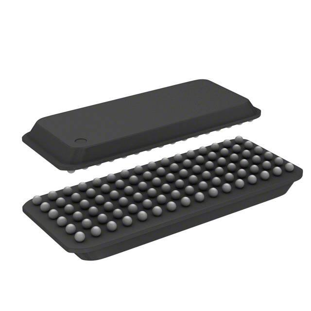
LFBGA96
74VCXH32245LB
)
s
t(
T&R
c
u
d
74VCXH32245LBR
o
r
P
This IC is intended for two-way asynchronous
communication between data buses: the direction
of data trasmission is determined by DIR input.
Any nG contol output governs four BUS
TRANSCEIVER. Output Enable input (nG) tied
together gives full 32-bit operation. When nG is
LOW, the output are on. When nG is HIGH, the
output are in high impedance state so that the
buses are effectively isolated. Bus hold on data
inputs is provided in order to eliminate the need for
external pull-up or pull-down resistor.
All inputs and outputs are equipped with
protection circuits against static discharge, giving
them 2KV ESD immunity and transient excess
voltage.
e
t
le
o
s
b
O
-
DESCRIPTION
The 74VCXH32245 is a low voltage CMOS QUAD
32-BIT
BUS
TRANSCEIVER
(3-STATE)
fabricated with sub-micron silicon gate and
five-layer metal wiring C2MOS technology. It is
ideal for 1.65 to 3.6 V applications; it can be
interfaced to 3.6V signal enviroment for both
inputs and outputs.
)
s
(
ct
LFBGA96
(Top and Bottom view)
r
P
e
LOGIC DIAGRAM
t
e
l
o
s
b
O
December 2001
1/10
This is preliminary information on a new product now in development are or undergoing evaluation. Details subject to change without notice.
�74VCXH32245
PIN CONNECTION
TERMINAL ASSIGNMENT
A
B
C
D
E
F
G
H
J
K
L
M
N
P
6
1A2
1A4
1A6
1A8
2A2
2A4
2A6
2A7
3A2
3A4
3A6
3A8
4A2
4A4
5
1A1
1A3
1A5
1A7
2A1
2A3
2A5
2A8
3A1
3A3
3A5
3A7
4A1
4A3
4
1G
GND
VCC
GND GND
VCC
GND
2G
3G
GND
VCC
GND GND
3
1DIR GND
VCC
GND GND
VCC
GND 2DIR 3DIR GND
VCC
2
1B1
1B3
1B5
1B7
2B1
2B3
2B5
2B8
3B1
3B3
1
1B2
1B4
1B6
1B8
2B2
2B4
2B6
2B7
3B2
3B4
INPUT AND OUTPUT EQUIVALENT CIRCUIT
)
s
(
ct
T
4A6
4A7
A45
4A8
GND
4G
GND GND
VCC
GND 4DIR
3B5
o
r
P
VCC
3B7
4B1
4B3
B45
4B8
3B6
3B8
4B2
4B4
4B6
4B7
e
t
le
o
s
b
O
-
)
s
t(
R
c
u
d
u
d
o
r
P
e
t
e
l
o
s
b
O
PIN DESCRIPTION
SYMBOL
nDIR
nA1 to nA8
nB1 to nB8
nG
GND
VCC
2/10
TRUTH TABLE
NAME AND FUNCTION
Directional Control
Data Inputs/Outputs
Data Inputs/Outputs
Output Enable Input
Ground (0V)
Positive Supply Voltage
INPUTS
FUNCTION
G
DIR
L
L
H
L
H
X
X : Don‘t Care
Z : High Impedance
A BUS
B BUS
OUTPUT INPUT
INPUT
OUTPUT
Z
Z
OUTPUT
Yn
A=B
B=A
Z
�74VCXH32245
ABSOLUTE MAXIMUM RATINGS
Symbol
VCC
Parameter
Value
Unit
Supply Voltage
-0.5 to +4.6
V
VI
DC Input Voltage
-0.5 to +4.6
V
VO
DC Output Voltage (VCC = 0V)
VO
DC Output Voltage (High or Low State) (note 1)
-0.5 to +4.6
V
-0.5 to VCC + 0.5
- 50
V
mA
IIK
DC Input Diode Current
IOK
DC Output Diode Current (note 2)
± 50
mA
IO
DC Output Current
± 50
mA
ICC or IGND DC VCC or Ground Current per Supply Pin
PD
Power Dissipation
Tstg
Storage Temperature
TL
Lead Temperature (10 sec)
± 100
mA
400
mW
-65 to +150
°C
300
°C
Absolute Maximum Ratings are those values beyond which damage to the device may occur. Functional operation under these conditions is
not implied
1) IO absolute maximum rating must be observed
2) VO < GND
c
u
d
RECOMMENDED OPERATING CONDITIONS
Symbol
VCC
ro
Parameter
Input Voltage
VO
Output Voltage (VCC = 0V)
VO
Output Voltage (High or Low State)
so
IOH, IOL
High or Low Level Output Current (VCC = 3.0 to 3.6V)
IOH, IOL
High or Low Level Output Current (VCC = 2.3 to 2.7V)
Top
dt/dv
P
e
let
Supply Voltage (note 1)
VI
Operating Temperature
(s)
Input Rise and Fall Time (note 2)
b
O
-
)
s
t(
Value
Unit
1.65 to 3.6
V
-0 to 3.6
V
0 to 3.6
V
0 to VCC
V
± 24
mA
± 18
mA
-40 to +85
°C
0 to 10
ns/V
t
c
u
1) Truth Table guaranteed: 1.2V to 3.6V
2) VIN from 0.8V to 2V at VCC = 3.0V
d
o
r
P
e
t
e
l
o
s
b
O
3/10
�74VCXH32245
DC SPECIFICATIONS (2.7V < VCC ≤ 3.6V unless otherwise specified)
Test Condition
Symbol
Parameter
Min.
2.0
High Level Input Voltage
2.7 to 3.6
VIL
Low Level Input Voltage
2.7 to 3.6
VOH
High Level Output Voltage
II
Low Level Output Voltage
Input Leakage Current
II(HOLD)
High Impedance Output Leakage
Current
Ioff
Power Off Leakage Current
ICC
Quiescent Supply Current
∆ICC
2.7
IO=-12 mA
2.2
3.0
IO=-18 mA
2.4
3.0
IO=-24 mA
2.2
2.7 to 3.6
IO=100 µA
0.2
2.7
IO=12 mA
0.4
3.0
IO=18 mA
0.4
3.0
IO=24 mA
0.55
2.7 to 3.6
VI = VCC or GND
±5
3
VI = 0.8V
75
3
VI = 2V
-75
3.6
VI = 0 to 3.6V
2.7 to 3.6
VI = VIH orVIL
VO = 0 to 3.6V
0
VI or VO = 0 to 3.6V
)
s
(
ct
r
P
e
t
e
l
o
s
b
O
4/10
e
t
le
c
u
d
V
)
s
t(
µA
µA
± 500
± 10
µA
10
µA
VI = VCC or GND
20
± 20
VIH = VCC-0.6V
750
so
V
V
VI or VO = VCC to 3.6V
b
O
-
2.7 to 3.6
u
d
o
0.8
2.7 to 3.6
3.6
ICC incr. per Input
V
VCC-0.2
o
r
P
Unit
Max.
IO=-100 µA
Input Hold Current
IOZ
-40 to 85 °C
VCC
(V)
VIH
VOL
Value
µA
µA
�74VCXH32245
DC SPECIFICATIONS (2.3V < VCC ≤ 2.7V unless otherwise specified)
Test Condition
Symbol
Parameter
Value
-40 to 85 °C
VCC
(V)
Min.
2.3 to 2.7
1.6
Max.
VIH
High Level Input Voltage
VIL
Low Level Input Voltage
2.3 to 2.7
VOH
High Level Output Voltage
2.3 to 2.7
IO=-100 µA
VCC-0.2
2.3
IO=-6 mA
2.0
2.3
IO=-12 mA
1.8
2.3
IO=-18 mA
1.7
2.3 to 2.7
IO=100 µA
0.2
2.3
IO=12 mA
0.4
VOL
II
Low Level Output Voltage
Input Leakage Current
II(HOLD)
Input Hold Current
IOZ
High Impedance Output Leakage
Current
Ioff
Power Off Leakage Current
ICC
Quiescent Supply Current
V
0.7
2.3
IO=18 mA
0.6
VI = VCC or GND
±5
2.3
VI = 0.8V
45
VI = 2V
-45
2.3 to 2.7
VI = VIH orVIL
VO = 0 to 5.5V
0
VI or VO = 0 to 3.6V
3.6
VI = VCC or GND
e
t
le
VI or VO = VCC to 3.6V
o
s
b
O
-
V
µA
)
s
t(
µA
c
u
d
o
r
P
V
V
2.3 to 2.7
2.3
Unit
± 10
µA
10
µA
20
± 20
µA
DYNAMIC SWITCHING CHARACTERISTICS (TA = 25°C, Input tr = tf = 2.0ns, CL = 30pF)
Test Condition
Symbol
Parameter
VCC
(V)
uc
(t s)
VOLP
Dynamic Peak Low Level Quiet
Output (note 1, 3)
VOLV
Dynamic Valley Low Level Quiet
Output (note 1, 3)
VOHV
Dynamic Valley High Level Quiet
Output (note 2, 3)
t
e
l
o
d
o
r
P
e
2.5
3.3
2.5
3.3
2.5
3.3
VIL = 0V, VIH = VCC
VIL = 0V, VIH = VCC
VIL = 0V, VIH = VCC
Value
TA = 25 °C
Min.
Typ.
0.6
0.8
-0.6
-0.8
1.9
2.2
Unit
Max.
V
V
V
1) Number of output defined as "n". Measured with "n-1" outputs switching from HIGH to LOW or LOW to HIGH. The remaining output is
measured in the LOW state.
2) Number of outputs defined as "n". Measured with "n-1" outputs switching from HIGH to LOW or LOW to HIGH. The remaining output is
measured in the HIGH state.
3) Parameters guaranteed by design.
s
b
O
5/10
�74VCXH32245
AC ELECTRICAL CHARACTERISTICS
Test Condition
Symbol
Parameter
tPLH tPHL
Propagation Delay Time
tPZL tPZH
Output Enable Time
tPLZ tPHZ
Output Disable Time
tOSLH
tOSHL
Value
-40 to 85 °C
VCC
(V)
Output To Output Skew Time
(note1, 2)
2.3 to
3.0 to
2.3 to
3.0 to
2.3 to
3.0 to
2.7 to
3.0 to
2.7
3.6
2.7
3.6
2.7
3.6
3.6
3.6
Min.
Max.
1.0
0.8
1.0
0.8
1.0
0.8
3.2
2.5
4.9
3.8
4.2
3.7
0.5
0.5
Unit
ns
ns
ns
ns
1) Skew is defined as the absolute value of the difference between the actual propagation delay for any two outputs of the same device switching in the same direction, either HIGH or LOW (tOSLH = | tPLHm - t PLHn|, tOSHL = | tPHLm - tPHLn|
2) Parameter guaranteed by design
CAPACITIVE CHARACTERISTICS
Test Condition
Symbol
Parameter
TA = 25 °C
VCC
(V)
o
r
P
Min.
Input Capacitance
2.5 or 3.3
VI = 0V or VCC
COUT
Output Capacitance
2.5 or 3.3
CPD
Power Dissipation Capacitance
(note 1)
2.5 or 3.3
VI = 0V or VCC
fIN = 10MHz
VI = 0V or VCC
CIN
c
u
d
Value
)
s
t(
b
O
-
so
e
t
le
Typ.
Unit
Max.
4
pF
8
pF
28
pF
1) CPD is defined as the value of the IC’s internal equivalent capacitance which is calculated from the operating current consumption without
load. (Refer to Test Circuit). Average operating current can be obtained by the following equation. ICC(opr) = CPD x VCC x fIN + ICC/16 (per
circuit)
)
s
(
ct
u
d
o
r
P
e
t
e
l
o
s
b
O
6/10
�74VCXH32245
TEST CIRCUIT
TEST
SWITCH
tPLH, tPHL
Open
tPZL, tPLZ (VCC = 3.0 to 3.6V)
6V
c
u
d
tPZL, tPLZ (VCC = 2.3 to 2.7V)
2VCC
tPZH, tPHZ
GND
CL = 30 pF or equivalent (includes jig and probe capacitance)
RL = R1 = 500Ω or equivalent
RT = ZOUT of pulse generator (typically 50Ω)
e
t
le
WAVEFORM SYMBOL VALUE
Symbol
o
s
b
O
-
3.0 to 3.6V
VIH
VM
(s)
VX
ct
VY
u
d
o
)
s
t(
o
r
P
VCC
2.3 to 2.7V
2.7V
VCC
1.5V
VCC/2
VOL +0.3V
VOL +0.15V
VOL -0.3V
VOL -0.15V
r
P
e
t
e
l
o
s
b
O
7/10
�74VCXH32245
WAVEFORM 1: PROPAGATION DELAY (f=1MHz; 50% duty cycle)
c
u
d
o
r
P
WAVEFORM 2: OUTPUT ENABLE AND DISABLE TIME (f=1MHz; 50% duty cycle)
e
t
le
)
s
(
ct
u
d
o
r
P
e
t
e
l
o
s
b
O
8/10
o
s
b
O
-
)
s
t(
�74VCXH32245
LFBGA96 MECHANICAL DATA
mm.
mils
DIM.
MIN.
TYP
MAX.
MIN.
TYP.
MAX.
A
13.40
13.60
527.5
535.4
B
5.40
5.60
212.6
220.5
C
1.6
63.0
D
0.5
19.7
E
F
0.8
0.85
31.5
0.95
33.5
37.4
c
u
d
e
t
le
)
s
(
ct
)
s
t(
o
r
P
o
s
b
O
-
u
d
o
r
P
e
t
e
l
o
s
b
O
9/10
�74VCXH32245
c
u
d
e
t
le
)
s
(
ct
)
s
t(
o
r
P
o
s
b
O
-
u
d
o
r
P
e
t
e
l
o
s
b
O
Information furnished is believed to be accurate and reliable. However, STMicroelectronics assumes no responsibility for the
consequences of use of such information nor for any infringement of patents or other rights of third parties which may result from
its use. No license is granted by implication or otherwise under any patent or patent rights of STMicroelectronics. Specifications
mentioned in this publication are subject to change without notice. This publication supersedes and replaces all information
previously supplied. STMicroelectronics products are not authorized for use as critical components in life support devices or
systems without express written approval of STMicroelectronics.
© The ST logo is a registered trademark of STMicroelectronics
© 2001 STMicroelectronics - Printed in Italy - All Rights Reserved
STMicroelectronics GROUP OF COMPANIES
Australia - Brazil - Canada - China - Finland - France - Germany - Hong Kong - India - Israel - Italy - Japan - Malaysia - Malta - Morocco
Singapore - Spain - Sweden - Switzerland - United Kingdom - United States.
© http://www.st.com
10/10
�
很抱歉,暂时无法提供与“74VCXH32245LBR”相匹配的价格&库存,您可以联系我们找货
免费人工找货