ACS108-6S
AC switch family Transient voltage protected AC Switch (ACS™)
Main product characteristics
IT(RMS) VDRM/VRRM IGT
■ ■
0.8 A 600 V 10 mA
COM
Overvoltage protection by crowbar technology High noise immunity - static dV/dt > 500 V/µs
G COM OUT
COM OUT G
SOT-223 ACS108-6SN
TO-92 ACS108-6SA
Applications
■ ■
AC ON/OFF static switching in appliances and industrial control systems Drive of low power high inductive or resistive loads like: – relay, valve, solenoid, – dispenser, door lock – pump, fan, micro-motor
Description
The ACS108-6S belongs to the AC line switch family. This high performance switch can control a load of up to 0.8A. The ACS108-6S switch includes an overvoltage crowbar structure to absorb the overvoltage energy, and a gate level shifter driver to separate the digital controller from the main switch. It is triggered with a negative gate current flowing out of the gate pin.
Benefits
■ ■ ■ ■ ■
Needs no external protection snubber or varistor. Enables equipment to meet IEC 61000-4-5. Reduces component count by up to 80%. Interfaces directly with the micro-controller. Common package tab connection supports connection of several alternating current switches (ACS) on the same cooling pad. Integrated structure based on ASD(a) technology
Functional diagram
OUT
■
G
Order code
Part number ACS108-6SA ACS108-6SA-TR ACS108-6SA-AP ACS108-6SN-TR Marking ACS1086S ACS1086S ACS1086S ACS1086S OUT G COM
COM
Common drive reference to connect to the mains Output to connect to the load. Gate input to connect to the controller through gate resistor
a. ASD: Application Specific Devices
TM: ACS is a trademark of STMicroelectronics
June 2006
Rev 2
www.st.com
1/11
�Characteristics
ACS108-6S
1
Table 1.
Symbol
Characteristics
Absolute maximum ratings (Tamb = 25 °C, unless otherwise specified)
Parameter TO-92 Tlead = 75 °C Tamb = 75 °C Tamb = 61 °C t = 16.7 ms t = 20 ms tp = 10 ms f = 120 Hz Tj = 125 °C Tj = 25 °C tp = 20 µs Tj = 125 °C Tj = 125 °C Tj = 125 °C 0.45 7.6 A f = 50 Hz 7.3 0.38 100 2 1 10 0.1 -40 to +150 -30 to +125 A2s A/µs kV A V W °C Value 0.8 A Unit
IT(RMS)
RMS on-state current (full sine wave)
SOT-223 TO-92
ITSM I²t dI/dt VPP IGM VGM PG(AV) Tstg Tj
Non repetitive surge peak on-state current (full cycle sine wave, Tj initial = 25 °C) I²t Value for fusing Critical rate of rise of on-state current IG = 2xIGT, tr ≤ 100 ns Non repetitive line peak mains voltage(1) Peak gate current Peak positive gate voltage Average gate power dissipation Storage junction temperature range Operating junction temperature range
f = 60 Hz
1. according to test described by IEC 61000-4-5 standard and Figure 16
Table 2.
Symbol IGT (1) VGT VGD IH (2) IL(2) dV/dt (2) (dI/dt)c (2) VCL
Electrical characteristics (Tj = 25 °C, unless otherwise specified)
Test conditions VOUT = 12 V, RL = 33 Ω VOUT = VDRM, RL =3.3 kΩ, Tj = 125 °C IOUT = 100 mA IG = 1.2 x IGT VOUT = 67% VDRM, gate open, Tj = 125 °C Without snubber (15 V/µs), turn-off time ≤ 20 ms, Tj = 125 °C ICL = 0.1 mA, tp = 1 ms, Tj = 125 °C Quadrant II - III II - III II - III MAX MAX MIN MAX MAX MIN MIN MIN Value 10 1 0.15 25 30 500 0.3 650 Unit
mA V V mA mA V/µs A/ms V
1. minimum IGT is guaranteed at 10% of IGT max 2. for both polarities of OUT referenced to COM
2/11
�ACS108-6S Table 3.
Symbol VTM (1) VTO RD
(1) (1)
Characteristics Static electrical characteristics
Test conditions ITM= 1.1 A, tp = 500 µs Tj = 25 °C Tj = 125 °C Tj = 125 °C Tj = 25 °C VOUT = 600 V MAX Tj = 125 °C 0.2 mA MAX MAX MAX Value 1.3 0.90 300 2 Unit V V mΩ µA
IDRM IRRM
1. for both polarities of OUT referenced to COM
Table 4.
Symbol Rth (j-l) Rth (j-l) Rth (j-a)
Thermal resistance
Parameter Junction to lead (AC) Junction to tab (AC) Junction to ambient S = 5 cm² SOT-223 60 TO-92 SOT-223 TO-92 Value 60 25 °C/W 150 Unit
Figure 1.
P (W)
Maximum power dissipation Figure 2. vs RMS on-state current (full cycle)
1.0 0.9
RMS on-state current vs ambient temperature (full cycle)
0.90 0.80 0.70 0.60 0.50
IT(RMS) (A)
ACS108-6SN (with 5cm² copper surface under tab)
0.8 0.7 0.6 0.5
ACS108-6SA
0.40 0.30 0.20 0.10 0.00 0.00
180°
0.4 0.3 0.2 0.1 0.0
0.10 0.20 0.30 0.40 0.50 0.60 0.70 0.80
IT(RMS) (A)
Tamb °C
0 25 50 75 100 125
3/11
�Characteristics
ACS108-6S
Figure 3.
Relative variation of junction to ambient thermal impedance vs pulse duration and package
Figure 4.
Relative variation of gate trigger current, holding current and latching current vs junction temperature
K=[Zth(j-a) /Rth(j-a) ]
1.E+00
1.E-01
TO-92
SOT-223
tP (S)
1.E-02 1.E-03 1.E-02 1.E-01 1.E+00 1.E+01 1.E+02 1.E+03
2.8 2.6 2.4 2.2 2.0 1.8 1.6 1.4 1.2 1.0 0.8 0.6 0.4 0.2 0.0
IGT, IH, IL [T j] / IGT, IH, IL [T j=25°C]
IGT
IL & IH
Tj(°C) -40 -30 -20 -10 0 10 20 30 40 50 60 70 80 90 100 110 120 130
Figure 5.
Non repetitive surge peak on-state Figure 6. current vs number of cycles
Non repetitive surge peak on-state current for a sinusoidal pulse with width tp
很抱歉,暂时无法提供与“ACS108-6SA”相匹配的价格&库存,您可以联系我们找货
免费人工找货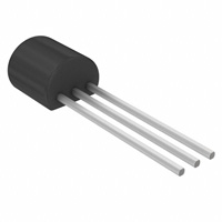


 工商网监
湘ICP备2023018690号
工商网监
湘ICP备2023018690号
