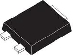
ACS108-8SUN
Overvoltage protected AC switch (ACS™)
Datasheet − production data
Description
COM
The ACS108-8SUN belongs to the AC line switch
range (built with A.S.D.® technology).This high
performance switch can control a load of up to
0.8 A.
OUT
The ACS108-8SUN switch includes an
overvoltage crowbar structure to absorb the
overvoltage energy and a gate level shifter driver
to separate the digital controller from the main
switch. It is triggered with a negative gate current
flowing out of the gate pin.
G
SMBflat-3L
Features
• Less footprint area than SOT-223 (saves PCB)
•
ECOPACK®2
Figure 1. Functional diagram
OUT
compliant component
• Thinner option versus SOT-223 (1.1 mm max.
thickness)
• Enables equipment to meet IEC 61000-4-5
G
• High noise immunity against static dV/dt and
IEC 61000-4-4 burst
• Overvoltage protection by crowbar technology
COM
• Needs no external protection snubber or
varistor
OUT
G
• Reduces component count by up to 80% and
Interfaces directly with the micro-controller
• VCL gives headroom before clamping then
crowbar action
• Common package tab connection supports
connection of several alternating current
switches on the same cooling pad
COM
Common drive reference to connect
to the mains
Output to connect to the load.
Gate input to connect to the controller
through gate resistor
Table 1. Device summary
Symbol
Value
Unit
IT(RMS)
0.8
A
VDRM / VRRM
800
V
IGT
10
mA
Applications
• Alternating current on/off static switching in
appliances and industrial control systems
• Drive of low power high inductive or resistive
loads like:
– relay, valve, solenoid, dispenser,
– pump, fan, low power motor, door lock,
– lamp
July 2014
This is information on a product in full production.
®: ECOPACK2 is a registered trademark of
STMicroelectronics
TM: ACS is a trademark of STMicroelectronics
®: A.S.D. is a registered trademark of STMicroelectronics
DocID022948 Rev 1
1/12
www.st.com
12
�Characteristics
1
ACS108-8SUN
Characteristics
Table 2. Absolute maximum ratings (Tamb = 25 °C, unless otherwise specified)
Symbol
Value
Unit
S = 0.5 cm² Tamb = 75 °C
0.45
A
Ttab = 113 °C
0.8
A
F = 60 Hz
t = 16.7 ms
13.7
F = 50 Hz
t = 20 ms
13
I²t Value for fusing
tp = 10 ms
1.1
A2s
dI/dt
Critical rate of rise of on-state current
F = 120 Hz
IG = 2xIGT, tr ≤ 100 ns
Tj = 125 °C
100
A/µs
VPP
Non repetitive line peak pulse mains voltage(1)
Tj = 25 °C
2
kV
IGM
Peak gate current
Tj = 125 °C
1
A
VGM
Peak positive gate voltage
Tj = 125 °C
10
V
Average gate power dissipation
Tj = 125 °C
0.1
W
-40 to +150
-30 to +125
°C
IT(RMS)
Parameter
On-state rms current (full sine wave)
Non repetitive surge peak on-state
current (full cycle sine wave,
Tj initial = 25 °C)
ITSM
I2t
PG(AV)
Tstg
Tj
A
tp = 20 µs
Storage junction temperature range
Operating junction temperature range
1. according to test described by IEC 61000-4-5 standard and Figure 19
Table 3. Electrical characteristics (Tj = 25 °C, unless otherwise specified)
Symbol
IGT(1)
VGT
VGD
Test conditions
VOUT = 12 V, RL = 33 Ω
VOUT = VDRM, RL =3.3 kΩ, Tj = 125 °C
Value
Unit
II - III
Max.
10
mA
II - III
Max.
1
V
II - III
Min.
0.15
V
IH
IOUT = 100 mA
Max.
10
mA
IL
IG = 1.2 x IGT
Max.
25
mA
VOUT = 402 V, gate open, Tj = 125 °C
Min.
2000
V/µs
VOUT = 536 V, gate open, Tj = 125 °C
Min.
400
V/µs
Without snubber (15 V/µs), turn-off time ≤ 20 ms, Tj = 125 °C
Min.
2
A/ms
ICL = 0.1 mA, tp = 1 ms, Tj = 125 °C
Min.
850
V
dV/dt
(dI/dt)c
VCL
1. Minimum IGT is guaranteed at 10% of IGT max
2/12
Quadrant
DocID022948 Rev 1
�ACS108-8SUN
Characteristics
Table 4. Static electrical characteristics
Symbol
Test conditions
VTM (1)
Value
Unit
ITM = 1.1 A, tp = 500 µs
Tj = 25 °C
Max.
1.3
V
VTO
(1)
Threshold voltage
Tj = 125 °C
Max.
0.85
V
RD
(1)
Dynamic resistance
Tj = 125 °C
Max.
300
mΩ
2
µA
0.2
mA
IDRM
IRRM
Tj = 25 °C
VOUT = VDRM = VRRM
Max.
Tj = 125 °C
1. For both polarities of OUT referenced to COM
Table 5. Thermal resistance
Symbol
Parameter
Rth (j-t)
Junction to tab (AC)
Rth (j-a)
Junction to ambient
Value
Max.
14
Max.
130
Unit
°C/W
S = 0.5 cm²
Figure 2. Maximum power dissipation
versus on-state rms current (full cycle)
Figure 3. On-state rms current versus tab
temperature (full cycle)
P (W)
0.90
IT(RMS)(A)
0.9
0.80
� = 180°
0.8
0.70
SMBFlat - 3L
0.7
0.60
0.6
� = 180°
0.50
0.5
0.40
0.4
0.30
0.3
0.20
180°
0.2
�
0.10
�
IT(RMS) (A)
0.00
0.00
0.1
0.10
0.20
0.30
0.40
0.50
0.60
0.70
0.80
Figure 4. On-state rms current versus ambient
temperature (free air convection)
IT(RMS)(A)
0.9
TTAB(°C)
0.0
0
25
75
1.00
0.6
125
K=[Zth/Rth]
Zth(j-c)
Zth(j-a)
SMBflat-3L
Copper surface
area = 5 cm²
0.7
100
Figure 5. Relative variation of thermal
impedance junction to ambient versus pulse
duration
� = 180°
0.8
50
SMBflat-3L
Copper surface
area = 0.5 cm²
0.5
0.10
0.4
0.3
0.2
Single layer Printed
circuit board FR4
0.1
SMBFlat-3L
Copper surface
area = 5cm²
Tp(s)
Ta(°C)
Natural convection
0.0
0.01
0
25
50
75
100
125
1.0E-03
DocID022948 Rev 1
1.0E-02
1.0E-01
1.0E+00
1.0E+01
1.0E+02
1.0E+03
3/12
�Characteristics
ACS108-8SUN
Figure 6. Relative variation of holding and
latching current versus junction temperature
IH, IL [T j] / IH, IL [T j=25 °C]
Figure 7. Relative variation of IGT and VGT
versus junction temperature
3.5
3.0
IGT, VGT [Tj] / IGT, VGT, [Tj =25 °C]
IGT Q2
3.0
2.5
IL
IGT Q3
2.5
2.0
2.0
1.5
IH
1.5
1.0
1.0
0.5
VGT Q2-Q3
0.5
Tj(°C)
Tj(°C)
0.0
0.0
-50
-25
0
25
50
75
100
Figure 8. Surge peak on-state current versus
number of cycles
14
13
12
11
10
9
8
7
6
5
4
3
2
1
0
-50
125
-25
0
25
50
75
100
125
Figure 9. Non repetitive surge peak on-state
current for a sinusoidal pulse, and
corresponding value of I²t
IT(RMS)(A)
ITSM(A), I²t (A²s)
1.E+03
Tj initial = 25°C
t = 20 ms
ITSM
1.E+02
One cycle
Non repetitive
Tj initial = 25 °C
1.E+01
SMBFlat-3L
Repetitive
TTAB= 113 °C
1.E+00
I²t
t p(ms)
Number of cycles
1.E-01
1
10
100
Figure 10. On-state characteristics (maximum
values)
100.00
0.01
1000
0.10
1.00
10.00
Figure 11. Relative variation of critical rate of
decrease of main current versus junction
temperature
ITM(A)
(dI/dt)c [Tj] / (dI/dt)c [Tj=125 °C]
2.5
2.0
10.00
1.5
1.0
1.00
Tj=125 °C
Tj max.:
Tj=25 °C
0.5
Vto = 0.85 V
VTM(V)
Tj (°C)
Rd = 300 mΩ
0.0
0.10
0.0
4/12
0.5
1.0
1.5
2.0
2.5
3.0
3.5
4.0
4.5
25
35
DocID022948 Rev 1
45
55
65
75
85
95
105
115
125
�ACS108-8SUN
Characteristics
Figure 12. Relative variation of static dV/dt
immunity versus junction temperature
IDRM /IRRM [Tj;V
dV/dt [Tj; V D = VR ] /dV/dt [Tj =125°C;V D = VR = 536 V]
13
Figure 13. Relative variation of leakage current
versus junction temperature
DRM/ VRRM ]/I DRM /IRRM
[Tj=125°C;800 V]
1.0E+00
Value above 5 kV
12
11
10
VD=VR=402V
9
1.0E-01
VDRM=VRRM=800 V
8
7
6
5
VD=VR=536V
4
1.0E-02
3
2
1
Tj (°C)
Tj(°C)
0
1.0E-03
25
50
75
100
125
Figure 14. Relative variation of critical rate of
decrease of main current (dl/dt)c versus
(dV/dt)c
5.0
25
50
75
100
125
Figure 15. Thermal resistance junction to
ambient versus copper surface under tab
Rth(j-a) (°C/W)
(dI/dt)c [ (dV/dt) c ] / Specified (dI/dt) c
180
Tj =125 °C
SMBflat-3L
4.5
Printed circuit board FR4
copper thickness = 35 µm
160
4.0
3.5
140
3.0
120
2.5
2.0
100
1.5
80
1.0
0.5
60
50
(dV/dt)c (V/µs)
0.0
0.1
1.0
10.0
100.0
SCU(cm²)
0
DocID022948 Rev 1
1
2
3
4
5
5/12
�Alternating current line switch - basic application
2
ACS108-8SUN
Alternating current line switch - basic application
The ACS108-8SUN switch is triggered by a negative gate current flowing from the gate pin
G. The switch can be driven directly by the digital controller through a resistor as shown in
Figure 16.
Thanks to its overvoltage protection and turn-off commutation performance, the
ACS108-8SUN switch can drive a small power high inductive load with neither varistor nor
additional turn-off snubber.
Figure 16. Typical application program
Valve
ACS108-8SUN
Power supply
2.1
Vss
MCU
Vdd
AC Mains
Rg
VT
IT
Protection against overvoltage: the best choice is ACS
In comparison with standard Triacs, which are not robust against surge voltage, the
ACS108-8SUN is over-voltage self-protected, specified by the new parameter VCL. This
feature is useful in two operating conditions: in case of turn-off of very inductive load, and in
case of surge voltage that can occur on the electrical network.
2.1.1
High inductive load switch-off: turn-off overvoltage clamping
With high inductive and low RMS current loads the rate of decrease of the current is very
low. An overvoltage can occur when the gate current is removed and the OUT current is
lower than IH.
As shown in Figure 17 and Figure 18, at the end of the last conduction half-cycle, the load
current decreases (1). The load current reaches the holding current level IH (2), and the
ACS108-8SUN turns off (3). The water valve, as an inductive load (up to 15 H), reacts as a
current generator and an overvoltage is created, which is clamped by the ACS108-8SUN
(4). The current flows through the ACS108-8SUN avalanche and decreases linearly to zero.
During this time, the voltage across the switch is limited to the clamping voltage VCL. The
energy stored in the inductance of the load is dissipated in the clamping section that is
designed for this purpose. When the energy has been dissipated, the ACS108-8SUN
voltage falls back to the mains voltage value (5)(230 Vrms, 50 Hz).
6/12
DocID022948 Rev 1
�ACS108-8SUN
Alternating current line switch - basic application
Figure 17. Effect of the switching off of a
high inductive load - typical clamping
capability of ACS108-8SUN (Tamb = 25 °C)
Figure 18. Description of the different
steps during switching off of a high
inductive load
I OUT
4
1
VPEAK = V CL
I OUT
(5 mA/div)
3
1
2
IH
VOUT
(200 V/div)
3
4
VOUT
5
IH
VCL
2
5
100µs/div
2.1.2
Alternating current line transient voltage ruggedness
The ACS108-8SUN switch is able to withstand safely the ac line transients either by
clamping the low energy spikes or by breaking over under high energy shocks, even with
high turn-on current rises.
The test circuit shown in Figure 19 is representative of the final ACS108-8SUN application,
and is also used to test the ac switch according to the IEC 61000-4-5 standard conditions.
Thanks to the load limiting the current, the ACS108-8SUN switch withstands the voltage
spikes up to 2 kV above the peak line voltage. The protection is based on an overvoltage
crowbar technology. Actually, the ACS108-8SUN breaks over safely as shown in Figure 20.
The ACS108-8SUN recovers its blocking voltage capability after the surge (switch off back
at the next zero crossing of the current).
Such non-repetitive tests can be done 10 times on each ac line voltage polarity.
Figure 19. Overvoltage ruggedness test circuit for resistive and inductive loads with
conditions equivalent to IEC 61000-4-5 standards
+2 kV surge
generator
CC
Load
150 W 5 µH
ACS108-8SUN
OUT
Mains
voltage
230 V rms
50 Hz
G
VT
COM
IT
DocID022948 Rev 1
220 W
7/12
�Alternating current line switch - basic application
ACS108-8SUN
Figure 20. Typical current and voltage waveforms across the ACS108-8SUN (+2 kV
surge, IEC 61000-4-5 standard)
VT (200 V/div)
IT max = 17.2 A
dIT/dt = 72 A/us
IT (4 A/div)
500 ns/div
8/12
DocID022948 Rev 1
�ACS108-8SUN
3
Package information
Package information
•
Epoxy meets UL94, V0
•
Lead-free packages
In order to meet environmental requirements, ST offers these devices in different grades of
ECOPACK® packages, depending on their level of environmental compliance. ECOPACK®
specifications, grade definitions and product status are available at: www.st.com.
ECOPACK® is an ST trademark.
Figure 21. SMBflat-3L dimension definitions
A
e
D
c
b 2x
L2 2x
L 2x
L1
E E1
L1
L
L2
b4
Table 6. SMBflat-3L dimensions
Dimensions
Ref.
Millimeters
Min.
Typ.
Inches
Max.
Min.
Typ.
Max.
A
0.90
1.10
0.035
0.043
b
0.35
0.65
0.014
0.026
b4
1.95
2.20
0.07
0.087
c
0.15
0.40
0.006
0.016
D
3.30
3.95
0.130
0.156
E
5.10
5.60
0.201
0.220
E1
4.05
4.60
0.156
0.181
L
0.75
1.50
0.030
0.059
L1
0.40
0.016
L2
0.60
0.024
e
1.60
0.063
DocID022948 Rev 1
9/12
�Package information
ACS108-8SUN
Figure 22. SMBflat-3L footprint dimensions
5.84
(0.230)
0.51
(0.020)
2.07
(0.082)
2.07
(0.082)
0.51
(0.020)
1.20
(0.047)
3.44
(0.136)
millimeters
(inches)
10/12
DocID022948 Rev 1
1.20
(0.047)
�ACS108-8SUN
4
Ordering information
Ordering information
Figure 23. Ordering information scheme
ACS
1
08 - 8
S UN -TR
AC switch series
Number of switches
1 = 1 switch
Current
08 = 0.8 A rms
Voltage
8 = 800 V
Sensitivity
S = 10 mA
Package
UN = SMBflat-3L
Packing
TR = 13”, 5000 pieces
Table 7. Ordering information
5
Order code
Marking
Package
Weight
Base Qty
Delivery mode
ACS108-8SUN-TR
A088N
SMBflat-3L
0.2 g
2000
Tape and reel
Revision history
04
Table 8. Document revision history
Date
Revision
30-Jul-2014
1
Changes
Initial release.
DocID022948 Rev 1
11/12
�ACS108-8SUN
IMPORTANT NOTICE – PLEASE READ CAREFULLY
STMicroelectronics NV and its subsidiaries (“ST”) reserve the right to make changes, corrections, enhancements, modifications, and
improvements to ST products and/or to this document at any time without notice. Purchasers should obtain the latest relevant information on
ST products before placing orders. ST products are sold pursuant to ST’s terms and conditions of sale in place at the time of order
acknowledgement.
Purchasers are solely responsible for the choice, selection, and use of ST products and ST assumes no liability for application assistance or
the design of Purchasers’ products.
No license, express or implied, to any intellectual property right is granted by ST herein.
Resale of ST products with provisions different from the information set forth herein shall void any warranty granted by ST for such product.
ST and the ST logo are trademarks of ST. All other product or service names are the property of their respective owners.
Information in this document supersedes and replaces information previously supplied in any prior versions of this document.
© 2014 STMicroelectronics – All rights reserved
12/12
DocID022948 Rev 1
�