®
ACS120-7SB/SFP/ST
AC LINE SWITCH
ASD™ AC Switch Family
MAIN APPLICATIONS AC static switching in appliance control systems Drive of low power high inductive or resistive loads like - relay, valve, solenoid, dispenser - pump, fan, micro-motor - defrost heater
s s
COM
G OUT
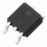
DPAK ACS120-7SB
FEATURES
s s
s
s
s
s
Blocking voltage : VDRM / VRRM = +/-700V Avalanche controlled : VCL typ = 1100 V Nominal conducting current : IT(RMS) = 2A Gate triggering current : IGT < 10 mA Switch integrated driver High noise immunity : static dV/dt >500V/µs
G COM OUT
G COM OUT
TO-220FPAB ACS120-7SFP
BENEFITS Needs no more external protection snubber or varistor Enables equipment to meet IEC 61000-4-5 Reduces component count up to 80 % Interfaces directly with the microcontroller Eliminates any gate kick back on the microcontroller Allows straightforward connection of several ACS™ on same cooling pad.
s s s s s s
TO-220AB ACS120-7ST
FUNCTIONAL DIAGRAM
OUT
DESCRIPTION The ACS120 belongs to the AC line switch family built around the ASD™ concept. This high performance switch circuit is able to control a load up to 2 A. The ACS™ switch embeds a high voltage clamping structure to absorb the inductive turn off energy and a gate level shifter driver to separate the digital controller from the main switch. It is triggered with a negative gate current flowing out of the gate pin.
S ON D
COM
G
1/11
April 2003 - Ed: 2A
�ACS120-7SB/SFP/ST
ABSOLUTE RATINGS (limiting values) For either positive or negative polarity of pin OUT voltage in respect to pin COM voltage Symbol
VDRM / VRRM IT(RMS)
Parameter
Repetitive peak off-state voltage RMS on-state current full cycle sine wave 50 to 60 Hz DPAK TO-220FPAB TO-220AB Tj = -10 °C Tc = 115 °C Tc = °C Tc = 115 °C F =50 Hz F =60 Hz tp = 10ms Tj = 125°C F = 120 Hz note 1
Value
700 2
Unit
V A
ITSM I2t dI/dt VPP Tstg Tj Tl
Non repetitive surge peak on-state current Tj initial = 25°C, full cycle sine wave Fusing capability Repetitive on-state current critical rate of rise IG = 10mA (tr < 100ns) Non repetitive line peak pulse voltage Storage temperature range Operating junction temperature range Maximum lead soldering temperature during 10s
20 11 2.2 50 2 - 40 to + 150 - 30 to + 125 260
A A A²s A/µs kV °C °C °C
Note 1: according to test described by IEC61000-4-5 standard & Figure 3.
GATE CHARACTERISTICS (maximum values) Symbol
PG (AV) IGM VGM
Parameter
Average gate power dissipation Peak gate current (tp = 20µs) Peak positive gate voltage (in respect to pin COM)
Value
0.1 1 5
Unit
W A V
THERMAL RESISTANCES Symbol
Rth (j-a) Junction to ambient
Parameter
S = 0.5cm² DPAK TO-220FPAB TO-220AB
Value
70 60 60 2.6 3.5 2.6
Unit
°C/W °C/W °C/W °C/W °C/W °C/W
Rth (j-l)
Junction to tab/lead for full cycle sine wave conduction
DPAK TO-220FPAB TO-220AB
S = Copper surface under Tab
2/11
�ACS120-7SB/SFP/ST
PARAMETER DESCRIPTION Parameter Symbol
IGT VGT VGD IH IL VTM VTO Rd IDRM / IRRM dV/dt (dV/dt)c (dI/dt)c VCL ICL Triggering gate current Triggering gate voltage Non-triggering gate voltage Holding current Latching current Peak on-state voltage drop On state threshold voltage On state dynamic resistance Maximum forward or reverse leakage current Critical rate of rise of off-state voltage Critical rate of rise of commutating off-state voltage Critical rate of decrease of commutating on-state current Clamping voltage Clamping current
Parameter description
ELECTRICAL CHARACTERISTICS For either positive or negative polarity of pin OUT voltage in respect to pin COM voltage. Symbol
IGT VGT VGD IH IL VTM VTO Rd IDRM / IRRM dV/dt (dI/dt)c VCL VOUT = 700V VOUT=12V (DC) VOUT=12V (DC)
Test Conditions
RL=140Ω RL=140Ω QII - QIII QII - QIII Tj=25°C Tj=25°C Tj=125°C Tj=25°C Tj=25°C tp=380µs Tj=25°C Tj=125°C Tj=125°C Tj=25°C Tj=125°C VOUT=460V gate open (dV/dt)c = 20V/µs ICL = 1mA tp=1ms Tj=110°C Tj=125°C Tj=25°C MAX MAX MIN MAX MAX MAX MAX MAX MAX MAX MIN MIN TYP
Values
10 1 0.15 45 65 1.3 0.85 200 2 200 500 1 1100
Unit
mA V V mA mA V V mΩ µA V/µs A/ms V
VOUT=VDRM RL=3.3kΩ IOUT= 100mA gate open IG= 20mA IOUT = 2.8A
3/11
�ACS120-7SB/SFP/ST
AC LINE SWITCH BASIC APPLICATION The ACS120 device is well adapted to Washing machine, dishwasher, tumble drier, refrigerator, air-conditioning systems, and cookware. It has been designed especially to switch on & off low power loads such as solenoid, valve, relay, dispenser, micro-motor, pump, fan and defrost heaters. Pin COM: Common drive reference to connect to the power line neutral Pin G: Switch Gate input to connect to the digital controller Pin OUT: Switch Output to connect to the load This ACS™ switch is triggered with a negative gate current flowing out of the gate pin G. It can be driven directly by the digital controller through a resistor as shown on the typical application diagram. Thanks to its thermal and turn off commutation performances, the ACS120 switch is able to drive with no turn off additional snubber an inductive load up to 2 A.
TYPICAL APPLICATION DIAGRAM
L LOAD
L
AC MAINS
M R
N
OUT
ACS120
S ON D
COM
G
ST72 MCU
- Vcc
HIGH INDUCTIVE SWITCH-OFF OPERATION At the end of the last conduction half-cycle, the load current reaches the holding current level IH , and the ACS™ switch turns off. Because of the inductance L of the load, the current flows then through the avalanche diode D and decreases linearly to zero. During this time, the voltage across the switch is limited to the clamping voltage VCL. The energy stored in the inductance of the load depends on the holding current IH and the inductance (up to 10 H); it can reach about 10 mJ and is dissipated in the clamping diode section. The ACS switch sustains the turn off energy because its clamping section is designed for that purpose.
4/11
�ACS120-7SB/SFP/ST
Fig. A: Turn-off operation of the ACS120 switch with an electro-valve: waveform of the pin OUT current IOUT and voltage VOUT. Fig. B: ACS120 switch static characteristic.
IOUT
IH VCL
VOUT
AC LINE TRANSIENT VOLTAGE RUGGEDNESS The ACS120 switch is able to sustain safely the AC line transient voltages either by clamping the low energy spikes or by breaking over under high energy shocks, even with high turn-on current rises. The test circuit of the figure C is representative of the final ACS application and is also used to stress the ACS switch according to the IEC 61000-4-5 standard conditions. Thanks to the load, the ACS switch sustains the voltage spikes up to 2 kV above the peak line voltage. It will break over safely even on resistive load where the turn on current rise is high as shown on figure D. Such non repetitive test can be done 10 times on each AC line voltage polarity. Fig. C: Overvoltage ruggedness test circuit for resistive and inductive loads according to IEC61000-4-5 standards. R = 150Ω, L = 10µH, VPP = 2kV. Fig. D: Current and Voltage of the ACS120 during IEC61000-4-5 standard test with R, L & VPP .
R
L
OUT ACSxx
S
SURGE VOLTAGE AC LINE & GENERATOR
VAC + V PP
D ON
COM
G
RG = 220Ω
5/11
�ACS120-7SB/SFP/ST
OTHER FIGURES Maximum power dissipation vs RMS on state current. RMS on-state current vs ambient temperature, case temperature Relative variation of thermal impedance junction to ambient vs pulse duration and package Relative variation of gate trigger current vs junction temperature Relative variation of holding, latching and gate current vs junction Relative variation of dV/dt vs Tj Relative variation of (dV/dt)c vs (di/dt)c Surge peak on-state current vs number of cycles Non repetitive surge peak on-state current for a sinusoidal pulse with tp
很抱歉,暂时无法提供与“ACS120-7SB-TR”相匹配的价格&库存,您可以联系我们找货
免费人工找货- 国内价格
- 1+12.87755
- 10+7.89230
- 100+5.93270